


INTEGRATED CIRCUITS
DATA SH EET
TZA1020; TZA1020A
Pre-amplifiers for CD-RW systems
Product specification
File under Integrated Circuits, IC01
2000 Oct 30

Philips Semiconductors Product specification
Pre-amplifiers for CD-RW systems TZA1020; TZA1020A
CONTENTS
1 FEATURES
2 GENERAL DESCRIPTION
3 QUICK REFERENCE DATA
4 ORDERING INFORMATION
5 BLOCK DIAGRAM
6 PINNING
7 FUNCTIONAL DESCRIPTION
7.1 Data amplifier
7.2 Normalizer
7.3 Wobble pre-processor
7.4 Beta detector
7.5 Alpha detector
7.6 Fast track count
7.7 Spot position measurement
8I
8.1 Addressing and data bytes
8.1.1 Write mode
8.1.2 Read mode
8.1.3 Control byte subaddress 00
8.1.4 Control byte subaddress 01
8.1.5 Control byte subaddress 02
8.1.6 Control byte subaddress 03
8.1.7 Control byte subaddress 04
8.1.8 Control byte subaddress 05
8.1.9 Control byte subaddress 06
8.1.10 Control byte subaddress 07
8.2 Characteristics of the I2C-bus
2
C-BUS PROTOCOL
9 LIMITING VALUES
10 THERMAL CHARACTERISTICS
11 CHARACTERISTICS
11.1 Transfer functions for normalizedservo signals
11.2 Laser power control signals (alpha circuit)
11.3 Wobble pre-processor
12 APPLICATION AND TEST INFORMATION
13 PACKAGE OUTLINE
14 SOLDERING
14.1 Introduction to soldering surface mount
packages
14.2 Reflow soldering
14.3 Wave soldering
14.4 Manual soldering
14.5 Suitability of surface mount IC packages for
wave and reflow soldering methods
15 DATA SHEET STATUS
16 DEFINITIONS
17 DISCLAIMERS
18 PURCHASE OF PHILIPS I2C COMPONENTS
2000 Oct 30 2
Philips Semiconductors Product specification
Pre-amplifiers for CD-RW systems TZA1020; TZA1020A
1 FEATURES
• Dataamplifierfor read speed up to twelve times nominal
data speed
• Normalized and filtered error signals for servo control
• Wobble pre-processor with switchable low-pass filter
• Calculation of signals for real-time laser power control
for write speed up to four times
• Calculation of signals for optimum laser calibration for
write speed up to four times
• Fast track count amplifier
• Spot position measurement for alignment of photo
diodes
• Reference voltage for laser controller
• On-chip band gap and DACs for accurate and
adjustable current/gain settings
• I2C-bus microcontroller interface for programmable
gain, speed switching and function selection
• All functions available for CD-R and CD-RW systems.
2 GENERAL DESCRIPTION
TZA1020 (AEGER2) is an analog pre-processor IC for
CD-RandCD-RWsystemswith 3-spots push-pull tracking
system. The IC interfaces directly to the photo diodes.
The device generates signals for laser power calibration
and laser power control during disc writing. Normalized
error signals are generated for servo control and wobble
detection. An HF current amplifier is implemented to
detect the actual HF data signal. The Fast Track Count
(FTC) amplifier generates a radial error signal to allow fast
track counting.
TZA1020A (AEGER2A) is similar to the TZA1020, except
for non-clamped MIRN, which allows operation with
IGUANA.
3 QUICK REFERENCE DATA
SYMBOL PARAMETER CONDITIONS MIN. TYP. MAX. UNIT
V
DD
V
SS
I
i(cd)
B
−3dB(norm)
positive supply voltage 4.5 5.0 5.5 V
negative supply voltage −5.5 −5.0 −4.5 V
central diode input current range 0 − 4000 µA
−3 dB bandwidth normalized
48 60 − kHz
error signals (servo)
B
−3dB(CAHF)
∆t
d(g)(CAHF)
−3 dB bandwidth pin CAHF Ci=12pF 17 −−MHz
group delay variations pin CAHF f = 0.1 to 12 MHz;
−−0.9 ns
Ci=12pF
G
I(CAHF)
current gain pin CAHF cdrwsel = 1 − 35 −
cdrwsel = 0 − 8.75 −
I
RREF
T
amb
reference current −−900 −µA
ambient temperature 0 − 70 °C
4 ORDERING INFORMATION
TYPE
NUMBER
TZA1020HP;
TZA1020HP/A
NAME DESCRIPTION VERSION
QFP44 plastic quad flat package; 44 leads (lead length 1.3 mm);
body 10 × 10 × 1.75 mm
PACKAGE
SOT307-2
2000 Oct 30 3
Philips Semiconductors Product specification
Pre-amplifiers for CD-RW systems TZA1020; TZA1020A
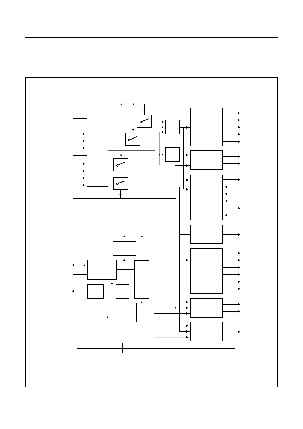
5 BLOCK DIAGRAM
handbook, full pagewidth
ERON
CAGAIN
SA1
SA2
SB1
SB2
C1
C2
C3
C4
AMON
15
11
4
8
5
9
10
3
6
7
14
INPUT
STAGE 3
DIODE
INPUT
STAGE 1
DIODE
INPUT
STAGE 2
TZA1020
TZA1020A
control
switches
control
currents
LPF 1
LPF 2
NORMALIZER
WOBBLE
PREPROCESSOR
ALPHA
DETECTOR
CURRENT
AMPLIFIER
35
36
37
34
38
27
26
22
21
20
19
24
25
23
FEN
REN
TLN
XDN
MIRN
CWBL
PPN
AINT
ALS
AINTON
ASTROBE
DALPHA
AZIN
CAHF
SDA
SCL
UOUT
RREF
12
13
1
2
V
DD1
I2C-BUS
INTERFACE
DRIVER
16
28
V
DD2
REGISTER
POR
BAND GAP
REFERENCE
30
V
V
SS1
DACs
18
29
GND117GND2
SS2
Fig.1 Block diagram.
BETA
DETECTOR
MEAS
FAST
TRACK
COUNT
44
43
42
39
40
41
32
33
31
MGR809
CALF
A1
A2
CALPF
HCA1
HCA2
MEAS1
MEAS2
RE
2000 Oct 30 4

Philips Semiconductors Product specification
Pre-amplifiers for CD-RW systems TZA1020; TZA1020A
6 PINNING
SYMBOL PIN DESCRIPTION
UOUT 1 reference voltage output
RREF 2 reference current input
C2 3 central photo diode current input
SA1 4 satellite photo diode current input
SB1 5 satellite photo diode current input
C3 6 central photo diode current input
C4 7 central photo diode current input
SA2 8 satellite photo diode current input
SB2 9 satellite photo diode current input
C1 10 central photo diode current input
CAGAIN 11 set-point laser power on disc,
current input
SDA 12 I
SCL 13 I
2
C-bus data input/output
2
C-bus clock input
AMON 14 alpha measurement on switch
(write/read state)
ERON 15 normalized error signals on switch
V
DD2
16 positive supply voltage 2
GND2 17 ground 2
V
SS2
18 negative supply voltage 2
ASTROBE 19 control signal sample-and-hold in
alpha measurement
AINTON 20 control signal integrator in alpha
measurement
ALS 21 DALPHA output enabled/disabled
AINT 22 integrator capacitor for alpha
measurement
CAHF 23 central aperture high-frequency
current output
DALPHA 24 alpha error signal for laser power
control
AZIN 25 set-point alpha control
SYMBOL PIN DESCRIPTION
PPN 26 normalized, balanced push-pull
signal voltage
CWBL 27 capacitor for EFM noise reduction
loop
V
DD1
28 positive supply voltage 1
GND1 29 ground 1
V
SS1
30 negative supply voltage 1
RE 31 fast track count signal voltage
output
MEAS1 32 combination of photo diode
currents for adjustment 1
MEAS2 33 combination of photo diode
currents for adjustment 2
XDN 34 normalized spot position error
current output
FEN 35 normalized focus error current
output
REN 36 normalized radial error current
output
TLN 37 normalized track-loss current
output
MIRN 38 mirror output (disc reflection)
current output
CALPF 39 capacitor to define CALF
bandwidth
HCA1 40 capacitor to define time constant
peak detector A1
HCA2 41 capacitor to define time constant
peak detector A2
A2 42 pit amplitude relative to CALF,
voltage output
A1 43 land amplitude relative to CALF,
voltage output
CALF 44 low-pass filtered aperture signal,
voltage output
2000 Oct 30 5
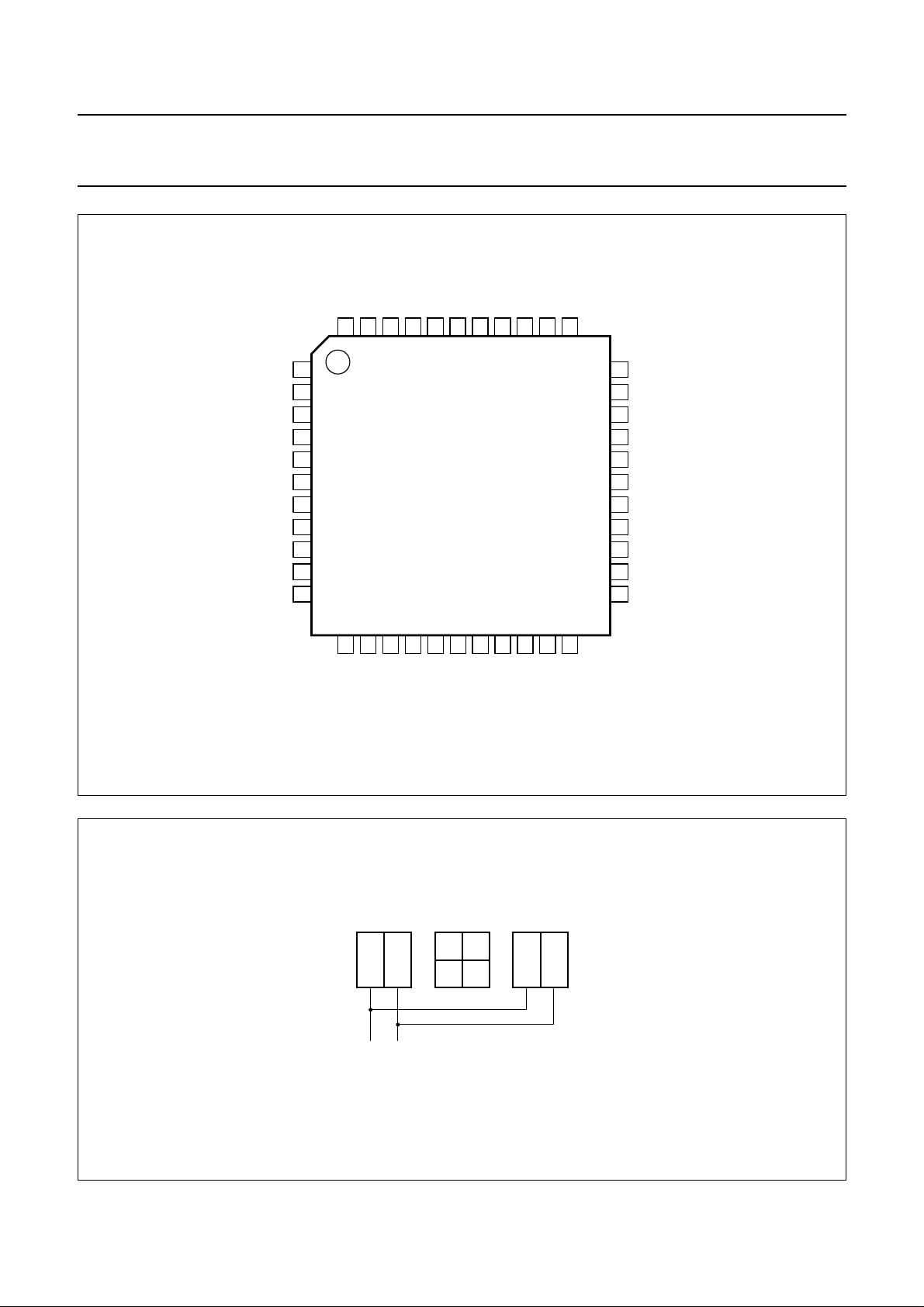
Philips Semiconductors Product specification
Pre-amplifiers for CD-RW systems TZA1020; TZA1020A
handbook, full pagewidth
CALF
44
A1
43
A2
42
HCA2
41
HCA1
40
MIRN
CALPF
39
38
TLN
37
REN
36
FEN
35
XDN
34
UOUT
RREF
C2
SA1
SB1
C3
C4
SA2
SB2
C1
CAGAIN
22
AINT
33
MEAS2
MEAS1
32
31
RE
V
30
GND1
29
V
28
CWBL
27
PPN
26
AZIN
25
24
DALPHA
CAHF
23
MGR810
SS1
DD1
1
2
3
4
5
6
7
8
9
10
11
12
13
SCL
SDA
TZA1020HP
TZA1020HP/A
14
15
16
V
ERON
AMON
DD2
17
GND2
18
V
SS2
19
20
AINTON
ASTROBE
21
ALS
Fig.2 Pin configuration.
handbook, halfpage
ACB
C1C4C2
SA1 SA2
S1 S2
Fig.3 Quadrant diode configuration.
2000 Oct 30 6
C3
SB1 SB2
MGR811

Philips Semiconductors Product specification
Pre-amplifiers for CD-RW systems TZA1020; TZA1020A
7 FUNCTIONAL DESCRIPTION
All functions are designed in such a way that a read speed
up to twelve times nominal speed is possible
(N = 1, 2, 4, 8 or 12). Recording speed up to four is
possible (N = 1, 2 or 4). The maximum recording speed
must be determined.
7.1 Data amplifier
The central diodes currents (C1 to C4) are fed to a high
bandwidth current amplifier. The gain of the current
amplifier can be switched by means of the I2C-bus
microcontroller interface to compensate for differences in
CD-R and CD-RW disc reflection. Data signals up to
twelve times nominal data speed can be read.
7.2 Normalizer
The currents from the central diodes (C1 to C4), the
currentfrom the satellite diodes (SA1, SA2, SB1 and SB2)
and the laser set-point current (CAGAIN) are (optionally
sampled) fed to the first low-pass filters with a bandwidth
of 60 kHz. The normalizing circuit generates error signals
for servo control that are independent of the diode current
level. The gain of the error signals is controlled by the
I2C-bus microcontroller interface. A dropout concealment
becomes active if the input current level is below a certain
threshold value. This threshold value is also controlled by
the I2C-bus.
7.3 Wobble pre-processor
The wobble signal of the pre-groove is detected by means
of the PPN signal. The currents from inputs C1 to C4 are
filtered and processed to provide optimal signal-to-noise
ratio. The bandwidth of the filter may be adapted to the
disc speed via the I2C-bus. The bandwidth of a noise
reduction loop is controlled by an external capacitor, the
I2C-bus interface controls the total operation of the
processor.
7.4 Beta detector
The beta detector generates signals necessary for the
symmetry detection of the HF signal. By measuring peak
values (A1 and A2) and average value of the signal
(CALF), an optimum laser writing power can be
determined. The gain of the measured values is controlled
by the I2C-bus. The time constant of the peak detectors
and bandwidth of the low-pass filtered aperture signal can
also be adapted to the disc speed by the I2C-bus.
7.5 Alpha detector
The alpha detector determines a parameter called ‘alpha’
during disc writing. Alpha must be kept constant to allow
recording over a fingerprint or black dot. The definition of
alpha is different for CD-R and CD-RW; for CD-R the light
absorption of the disc is measured, for CD-RW alpha is
determined by actual laser power and disc reflection. The
gain of the measured signals and the CD-R and CD-RW
selection is performed by the I2C-bus.
7.6 Fast track count
The fast track count circuit generates a Radial Error (RE)
signal for fast track counting. A gain switch compensates
for difference in CD-R and CD-RW disc reflection.
7.7 Spot position measurement
To allow alignment of photo diodes via the TZA1020, a
number of linear combinations of input currents can be
realized (MEAS1 and MEAS2). Selection of the actual
combination is performed by the I2C-bus.
2000 Oct 30 7

Philips Semiconductors Product specification
Pre-amplifiers for CD-RW systems TZA1020; TZA1020A
8I2C-BUS PROTOCOL
8.1 Addressing and data bytes
Full control of the TZA1020 is accomplished via the 2-wire I2C-bus. Up to 400 kbits/s bus speed can be used in
accordance with the I2C-bus fast-mode specification.
For programming the device (write mode) eight data byte registers are available/addressable via eight subaddresses.
Automatic subaddress incrementing enables the writing of successive data bytes in one transmission. During power-on,
data byte registers are reset to a default state by use of a Power-On Reset (POR) circuit whose signal is derived from
the internally generated I2C-bus supply voltage (V
For reading from the device (read mode) one data byte register is available without subaddressing.
8.1.1 WRITE MODE
Table 1 Slave address; 34H
Slave address 0 0 1 1 0 1 0 0
Table 2 Subaddress 00H to 07H
Subaddress 0
(1)
(1)
0
).
SS1
(1)
0
(1)
0
0 0/1 0/1 0/1
Note
1. The use of subaddresses F0H to F7H (11110XXX) instead of 00H to 07H (00000XXX) disables the automatic
subaddress incrementing allowing continuous writing to a single data byte register (e.g. DAC testing).
Table 3 Overview of subaddresses
SUB
ADDR
POR
STATE
DATA BYTES
00H 00000000 alphactr2 alphactr1 alphactr0 alphagain4 alphagain3 alphagain2 alphagain1 alphagain0
01H 00000000 free algctr6 algctr5 algctr4 algct3 algctr2 algctr1 algctr0
02H 00000000 tlngain1 tlngain0 rengain negain4 negain3 negain2 negain1 negain0
03H 00000000 tmdac tlnlim1 tlnlim0 sumref4 sumref3 sumref2 sumref1 sumref0
04H 00000000 sdfine7 sdfine6 sdfine5 sdfine4 sdfine3 sdfine2 sdfine1 sdfine0
05H 00011111 lexton betactrl1 betactrl0 betascl4 betascl3 betascl2 betascl1 betascl0
06H 01100000 free ppnctrl1 ppnctrl0 ppnscl4 ppnscl3 ppnscl2 ppnscl1 ppnscl0
07H 00000000 porr free urefsel cdrwsel lpsel1 lpsel0 meassel1 meassel0
8.1.2 R
EAD MODE
Table 4 Slave address; 35H
Slave address 0 0 1 1 0 1 0 1
Table 5 Read byte
Read byte por
(1)
(2)
0
(2)
0
(2)
0
(2)
0
(2)
0
(2)
0
(2)
0
Notes
1. In read mode the actual POR status can be read.
2. The state of unused read bits should not be relied upon; their state may be changed during development.
2000 Oct 30 8

Philips Semiconductors Product specification
Pre-amplifiers for CD-RW systems TZA1020; TZA1020A
8.1.2.1 Examples of valid transmissions to and from the TZA1020
Write: START - 34H - 00H - Data_for_00 - STOP
Write with auto-increment: START - 34H - 00H - data_for_00 - data_for_01 - data_for_02 - STOP
Auto-increment ‘wrap around’: START - 34H - 07H - data_for_07 - data_for_00 - data_for_01 - STOP
Write without auto-increment: START - 34H - F5H - data_for_05 - data_for_05 - data_for_05 - STOP
Read: START - 35H - data_from_ IC - STOP.
8.1.3 CONTROL BYTE SUBADDRESS 00
Table 6 Control bits for alphactrl
alphactrl2 alphactrl1 alphactrl0
0 0 0 0.50
0 0 1 0.33
0 1 0 0.25
0 1 1 0.20
1 0 0 0.17
1 0 1 0.14
1 1 0 0.12
1 1 1 0.11
Table 7 Control bits for alphagain-DAC; note 1
alphagain4 alphagain3 alphagain2 alphagain1 alphagain0 CURRENT alphagain-DAC
0 0 0 0 0 3.125 µA
0 0 0 0 1 6.250 µA
0 0 0 1 0 9.375 µA
:
code
1 1 1 0 1 93.750 µA
1 1 1 1 0 96.900 µA
11111 100µA
GAIN INPUT CURRENT
ALPHA DETECTOR
:
100 µA (code + 1)/32
Note
1. The currents of all DACs is controlled by reference current (I
2000 Oct 30 9
). The given currents are valid at I
RREF
RREF
= −900 µA.

Philips Semiconductors Product specification
Pre-amplifiers for CD-RW systems TZA1020; TZA1020A
8.1.4 CONTROL BYTE SUBADDRESS 01
Table 8 Control byte for algctrl switch functions
algctr6 algctr5 algctr4 algctr3 algctr2 algctr1 algctr0 DESCRIPTION
0000000POR state
0 − 0 −−−−current gain alpha CD-R
Aoc = 0alpha CD-R circuit power-off
0 − 1 −−−−current gain alpha CD-R
Aoc = 1alpha CD-R circuit power-on
1 − 0 −−−−current gain alpha CD-R
Aoc = 3alpha CD-R circuit power-off
1 − 1 −−−−current gain alpha CD-R
Aoc = 4alpha CD-R circuit power-on
− 0 −−−−−alpha peak detector normal mode
− 1 −−−−−alpha peak detector to level (test)
−−−0−−−CD-RW mode 1
−−−1−−−CD-RW mode 2
−−−−0−−alpha CD-R
−−−−1−−alpha CD-RW
−−−−−0 0 DALPHA gain = 0.25
−−−−−0 1 DALPHA gain = 0.50
−−−−−1 0 DALPHA gain = 0.75
−−−−−1 1 DALPHA gain = 1.00
8.1.5 C
Table 9 Control bits for tlngain
Table 10 Control bits for rengain
ONTROL BYTE SUBADDRESS 02
tlngain1 tlngain0 GAIN TLN SIGNAL
0 0 1.5
0 1 3.0
1 0 4.5
1 1 6.0
rengain DESCRIPTION
0 1 normal
1 1.3 self test
2000 Oct 30 10

Philips Semiconductors Product specification
Pre-amplifiers for CD-RW systems TZA1020; TZA1020A
Table 11 Control bits for current negain-DAC; note 1
negain4 negain3 negain2 negain1 negain0 CURRENT negain-DAC
00000 3.125 µA
00001 6.250 µA
00010 9.375 µA
:
code
100 µA (code + 1)/32
11101 93.750 µA
11110 96.900 µA
11111 100µA
Note
1. The currents of all DACs is controlled by reference current (I
). The given currents are valid at I
RREF
8.1.6 CONTROL BYTE SUBADDRESS 03
Table 12 Control bit for tmdac
:
= −900 µA.
RREF
tmdac DESCRIPTION
0 DAC test off
1 DAC test on
Table 13 Control bits for tlnlimit
tlnlim1 tlnlim0 DESCRIPTION
0 0 clamp off
X 1 clamp on 1 (0.6 V; T
1 0 clamp on 2 (1.2 V; T
amb
amb
=25°C)
=25°C)
Table 14 Control bits for current sumref-DAC; note 1
sumref4 sumref3 sumref2 sumref1 sumref0 CURRENT sumref-DAC
00000 0.468 µA
00001 0.937 µA
00010 1.40 µA
:
code
15 µA (code + 1)/32
:
11101 14.06 µA
11110 14.53 µA
11111 15.00 µA
Note
1. The currents of all DACs is controlled by reference current (I
2000 Oct 30 11
). The given currents are valid at I
RREF
RREF
= −900 µA.
 Loading...