

Philips TZA1015 Service Manual

INTEGRATED CIRCUITS
DATA SH EET
TZA1015
Data amplifier and laser supply
circuit for CD and read-only optical
systems (HDALAS)
Preliminary specification
File under Integrated Circuits, IC01
1997 May 16

Philips Semiconductors Preliminary specification
Data amplifier and laser supply circuit for CD and
read-only optical systems (HDALAS)
FEATURES
• Six input buffer amplifiers with low-pass filtering and
virtually no offset
• Universal photodiode IC interface using internal
conversion resistors
• RF data amplifier with wide bandwidth designed for data
rates up to a maximum of 30×
• Programmable RF gain for CD-A/V, CD-R, CD-R/W and
CD-ROM applications
• Programmable RF bandwidth for optimal playability
• Radial error signal for fast track counting
• Programmable RF/Fast Track Count (FTC) gain for
optimal dynamic range
• Fully automatic laser control including stabilization and
on/off switch plus a separate supply for power efficiency
• Automatic monitor diode polarity selection
• Adjustable laser bandwidth and laser switch-on current
slope using external capacitor
• Protection circuit to prevent laser damage due to supply
voltage dip
• Optimized interconnection between data amplifier and
Philips’ digital signal processor family (CD7, ACE and
MACE)
• Wide supply voltage range
• Wide temperature range
• Low power consumption.
The device contains 6 transimpedance amplifiers to
amplify and filter the focus and radial photo diode voltage
input signals. The preamplifier forms a versatile,
programmable interface from voltage output CD
mechanisms to the Philips’ digital signal processor family.
The dynamic range of this preamplifier/processor
combination can be optimized for the LF servo and RF
data paths. The servo channel gain is set by the ADC
range of the processor. The RF data channel can be
programmed in the TZA1015 preamplifier.
The programmable RF bandwidth allows this device to be
used in CD-A/V applications or CD-R, CD-R/W and
CD-ROM applications with a data rate up to a maximum of
30×. The RF and LF gain can be adapted for CD-A/V,
CD-R and CD-ROM discs or CD-R/W discs by means of a
gain switch. In addition to this gain switch the RF gain is
programmable to guarantee optimal playability. In order to
enable minimal access time the TZA1015 generates a
Fast Track Count signal which enables the decoder (ACE
or MACE) to count the number of tracks during a track
jump.
The device can accommodate astigmatic, single Foucault
and double Foucault detectors and can be used with all
laser and N- or P-sub monitor diodes. The Automatic
Power Control circuit (APC) will maintain control over the
laser diode current. With an on-chip reference voltage
generator, a constant and stabilized output power is
ensured independent of ageing. A separate power supply
connection allows the internal power dissipation to be
reduced by connecting a low voltage supply.
TZA1015
GENERAL DESCRIPTION
The TZA1015 is a data amplifier and laser supply circuit for
3-beam pick-up detectors found in a wide range of CD and
read-only optical systems.
ORDERING INFORMATION
TYPE
NUMBER
TZA1015T SO28 plastic small outline package; 28 leads; body width 7.5 mm SOT136-1
1997 May 16 2
NAME DESCRIPTION VERSION
PACKAGE

Philips Semiconductors Preliminary specification
Data amplifier and laser supply circuit for CD and
TZA1015
read-only optical systems (HDALAS)
QUICK REFERENCE DATA
SYMBOL PARAMETER CONDITIONS MIN. TYP. MAX. UNIT
Supply
V
DD(RF,LF)
V
DD(LASER)
LF amplifiers
I
OS
B
(−3 dB)
RF amplifier
B
(−3 dB)
t
d(f)(RF)
Laser supply
I
o(LASER)(min)
V
i(mon)
Temperature range
T
oper
T
stg
supply voltage 4.5 5.0 5.5 V
laser supply voltage 3 − 5.5 V
channel matching −− 1 %FS
−3 dB bandwidth 65 90 115 kHz
−3 dB bandwidth programmable;
GARF = open-circuit
7.5 10 12.5 MHz
15 20 25 MHz
37 50 63 MHz
RF flatness delay −− 0.4 ns
minimum laser output current V
DD(LASER)
=3V −− 100 mA
monitor input voltage
N-type monitor − 0.150 − V
P-type monitor − V
DD(RF,LF)
− 0.150 − V
operating temperature 0 − 90 °C
storage temperature −65 − +150 °C
1997 May 16 3
Philips Semiconductors Preliminary specification
Data amplifier and laser supply circuit for CD and
read-only optical systems (HDALAS)
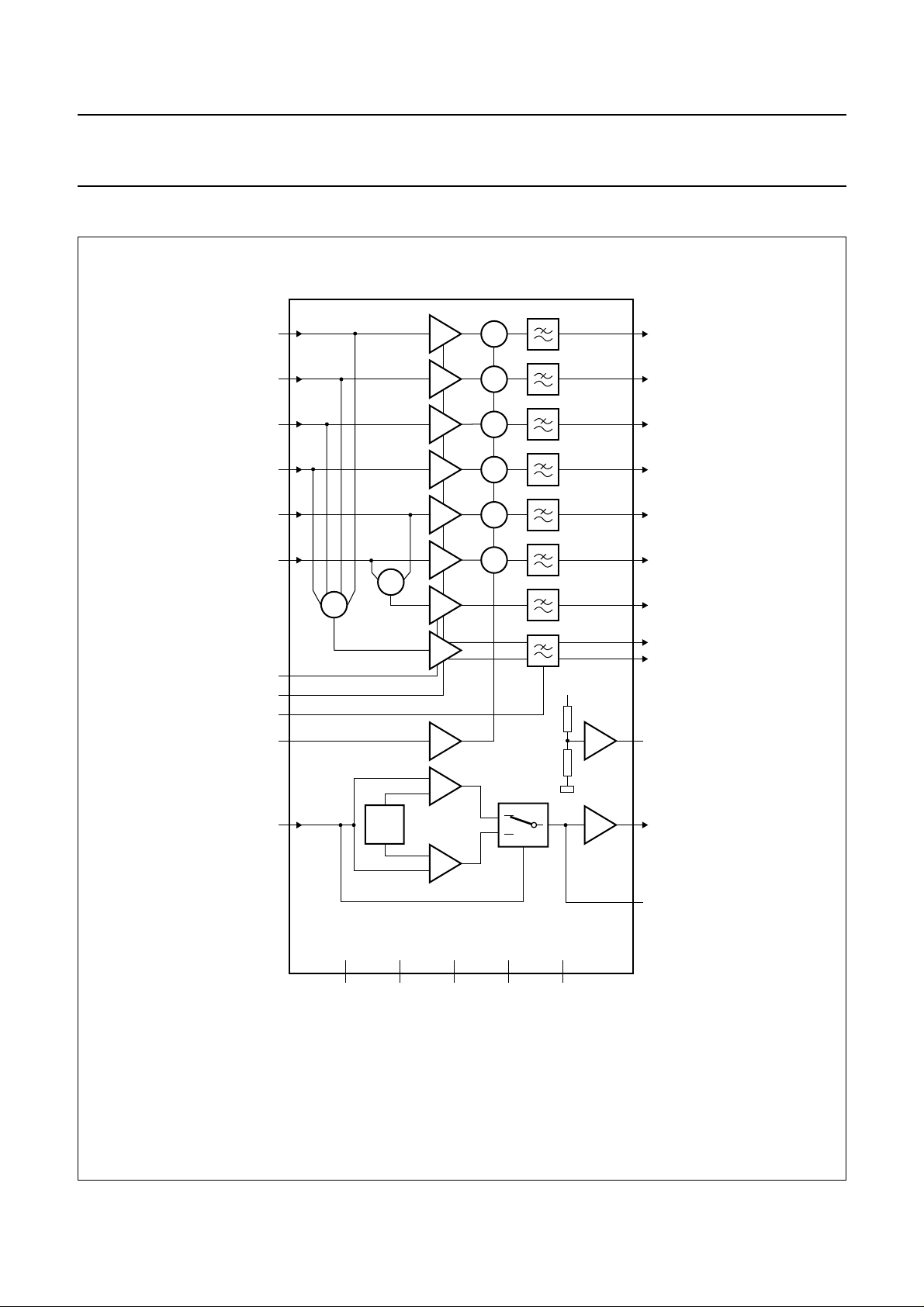
BLOCK DIAGRAM
handbook, full pagewidth
6
D1
D2
D3
D4
S5
S6
7
8
9
10
11
−
+
+
−
+
+
−
+
+
−
+
+
−
+
+
−
+
+
−
+
TZA1015
22
O1
21
O2
20
O3
19
O4
18
O5
17
O6
15
FTC
GARF
GSE
RFBWS
V
COM
MON
25
RFP
26
28
27
1
13
V
DD(LF)
RFN
14
V
ref
TZA1015
V/I
5
V
DD(RF)
V
GAP
V
DD(LF)
(1)
V/I
V
DD(L)
3
GND PWRON
2423
16
12
V/I
MGK356
2
LD
4
CFIL
(1) Band-gap reference voltage.
Fig.1 Block diagram.
1997 May 16 4
Philips Semiconductors Preliminary specification
Data amplifier and laser supply circuit for CD and
read-only optical systems (HDALAS)
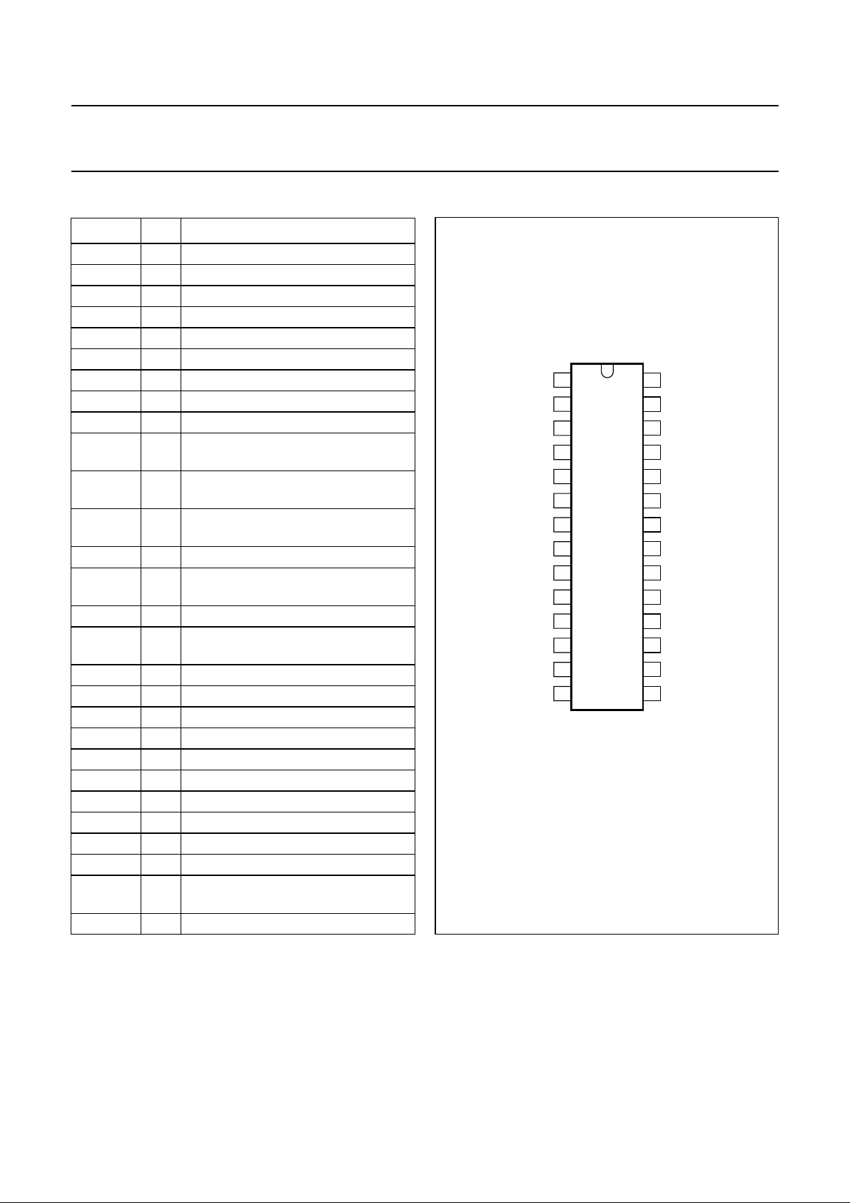
PINNING
SYMBOL PIN DESCRIPTION
RFBWS 1 RF amplifier bandwidth select
LD 2 current output to the laser diode
V
DD(L)
CFIL 4 external filter capacitor
MON 5 laser monitor diode input
D1 6 input photo diode amplifier 1 (central)
D2 7 input photo diode amplifier 2 (central)
D3 8 input photo diode amplifier 3 (central)
D4 9 input photo diode amplifier 4 (central)
S5 10 input photo diode amplifier 5
S6 11 input photo diode amplifier 6
V
DD(LF)
V
COM
V
ref
FTC 15 fast track count amplifier output
PWRON 16 power on/off switch (V
O6 17 output photo diode amplifier 6
O5 18 output photo diode amplifier 5
O4 19 output photo diode amplifier 4
O3 20 output photo diode amplifier 3
O2 21 output photo diode amplifier 2
O1 22 output photo diode amplifier 1
V
DD(RF)
GND 24 ground
RFP 25 positive output RF data amplifier
RFN 26 negative output RF data amplifier
GSE 27 gain select for CD, CD-R, CD-R/W;
GARF 28 gain adjust for RF and FTC amplifiers
3 laser supply voltage output
(satellite)
(satellite)
12 LF diode and FTC amplifier supply
voltage
13 common mode DC reference input
14 DC reference voltage for biasing of
Opto Electronic IC (OEIC)
bias
ref
generator always active)
23 RF amplifier supply voltage
RF and FTC amplifiers
handbook, halfpage
RFBWS
V
V
DD(LF)
DD(L)
CFIL
MON
V
COM
V
LD
D1
D2
D3
D4
S5
S6
ref
1
2
3
4
5
6
7
8
9
10
11
12
13
TZA1015
MGK355
Fig.2 Pin configuration.
TZA1015
GARF
28
GSE
27
RFN
26
RFP
25
GND
24
V
23
DD(RF)
O1
22
21
O2
O3
20
O4
19
O5
18
O6
17
PWRON
16
1514
FTC
1997 May 16 5

Philips Semiconductors Preliminary specification
Data amplifier and laser supply circuit for CD and
TZA1015
read-only optical systems (HDALAS)
CHARACTERISTICS
V
DD(LF)=VDD(RF)=VDD(LASER)
RFBWS = HIGH; DC input voltages at pins V
I
DD(LASER)(d)
= 50 mA; C
SYMBOL PARAMETER CONDITIONS MIN. TYP. MAX. UNIT
Supplies
V
DD(RF,LF)
V
DD(LASER)
I
DD(LF)
I
DD(RF)
I
DD(LASER)(d)
supply voltage 4.5 5.0 5.5 V
laser supply voltage 3 − 5.5 V
LF supply current − 13 − mA
RF supply current − 20 − mA
laser diode supply
current
I
q
quiescent supply
current
Input voltages
V
i(D1-D4,S5,S6)
input signal voltage
range (with respect
to V
COM
V
I(CM)
common mode DC
reference input
voltage range
= 5.0 V; T
= 1 nF; unless otherwise specified. Diode input voltages all with respect to V
CFIL
=25°C; PWRON = HIGH; GSE = LOW; GARF = open-circuit;
amb
, D1 to D4, S5 and S6 =1⁄2VDD; output voltage at pins O1 to O6 = 0 V;
COM
− 50 100 mA
PWRON = LOW −− 5.9 mA
all inputs;
0 − 0.6 V
GSE = LOW
)
all inputs;
0 − 0.15 V
GSE = HIGH
1.6 − V
DD(RF,LF)
.
COM
− 2.2 V
LF diode amplifiers
Z
CONV
conversion
impedance
central diodes,
D1 to D4
satellite diodes,
S5 and S6
I
o(LF)
output current
range
central diodes,
O1 to O4
satellite diodes,
O5 and O6
V
O(LF)
DC output voltage
range central and
satellite diodes
Z
i
input impedance
central diodes − 1.8 − pF
satellite diodes − 1.1 − pF
GSE = LOW 41 47 54 kΩ
GSE = HIGH 11.0 12.7 15.0 kΩ
GSE = LOW 80 92 104 kΩ
GSE = HIGH 21.0 24.5 28 kΩ
note 1
0 − 12 µA
0 − 6 µA
−0.2 − V
DD(RF,LF)
− 2.1 V
1997 May 16 6
 Loading...