

Philips TZA1000 Datasheet

INTEGRATED CIRCUITS
DATA SH EET
TZA1000
QIC read-write amplifier
Preliminary specification
Supersedes data of 1998 Mar 11
File under Integrated Circuits, IC01
1998 Mar 17

Philips Semiconductors Preliminary specification
QIC read-write amplifier TZA1000
FEATURES
• 3-wire serial interface for programming
• On-chip Digital-to-Analog Converters (DAC) for:
– MR (Magneto Resistive) sense bias current
– MR DC bias current
– Write current
• Low noise differential input stage: typically 0.65 nV/√Hz
(Zi=0Ω)
• Magnetic feedback circuit to handle large output signals
• MR DC bias current circuit
• Very fast write current rise and fall times with near
rail-to-rail voltage swing
• Maximum write current of 100 mA: ready for high
coercivity tape
• Low noise read amplifier for reading track height servo
signals with the write coil
• Very few external components required
• On board registers for easy format or bit rate selection
• Fast read-after-write recovery time
• Test circuit for yoke-type heads
• Switchable differentiator for yoke-type heads, with
programmable cut-off frequencies
• Anti-aliasing low-pass filter, with programmable cut-off
frequencies
• AGC (Automatic Gain Control) options: internally
(digitally) controlled, externally controlled or fixed gain
• Hold input for fast AGC freeze
• Input for fast reader/writer (track height servo) signal
selection
• Power fail detection on both 5 and 12 V lines (status can
be read from the read register)
• Write unsafe detection
• Provides an accurate reference voltage (for AD
conversion)
• Very simple interconnection with the SZA1000 QIC
digital equalizer
• +5 V ±10% and +12 V ±10% supply voltages
• Low power standby, active and test modes.
RELATED DOCUMENTS
• SZA1000 QIC digital equalizer data sheet
• Application notes for TZA1000 and SZA1000.
Both are available from Philips Semiconductors.
GENERAL DESCRIPTION
The TZA1000 is a single-chip read-write amplifier for
single-channel QIC (Quarter Inch Cartridge) systems with
MR heads. It can be used with both SIG (Sensor in Gap)and yoke-type MR heads and is designed to be used in
conjunction with the Philips SZA1000 digital equalizer IC
(although it can also function as a stand alone unit). This
combination is flexible enough to be used with all popular
tape backup formats including QIC 80, QIC 3010,
QIC 3020, QIC 3080, QIC 5010, Travan 1, Travan 2,
Travan 3 and Travan 4 and to be forward compatible with
their single channel successors.
QUICK REFERENCE DATA
SYMBOL PARAMETER CONDITIONS MIN. TYP. MAX. UNIT
V
DD1
V
DD2
V
DD3
I
DD1;IDD2
read circuit supply voltage 4.5 5 5.5 V
FB and write circuit supply voltage 4.5 5 5.5 V
sense current circuit supply voltage 10.8 12 13.2 V
read/FB and write circuit supply current
Read mode − 69 − mA
I
DD3
V
n(i)(eq)
f
clk
T
amb
T
j
R
th(j-a)
Write mode I
sense current circuit supply current I
equivalent input noise voltage Z
clock frequency −−24 MHz
recommended operating temperature 0 − 70 °C
recommended junction temperature 0 − 125 °C
thermal resistance from junction to ambient in free air − 66 − K/W
=30mA − 105 − mA
write
= 16 mA 15.0 16.2 19.0 mA
sense
=0Ω− 0.65 0.8 nV/√Hz
source
1998 Mar 17 2

Philips Semiconductors Preliminary specification
QIC read-write amplifier TZA1000
ORDERING INFORMATION
TYPE
NUMBER
TZA1000 SO24 plastic small outline package; 24 leads; body width 7.5 mm SOT137-1
NAME DESCRIPTION VERSION
PACKAGE
1998 Mar 17 3
This text is here in white to force landscape pages to be rotated correctly when browsing through the pdf in the Acrobat reader.This text is here in
_white to force landscape pages to be rotated correctly when browsing through the pdf in the Acrobat reader.This text is here inThis text is here in
white to force landscape pages to be rotated correctly when browsing through the pdf in the Acrobat reader. white to force landscape pages to be ...
1998 Mar 17 4
handbook, full pagewidth
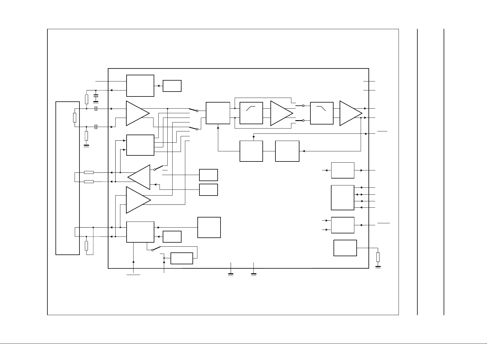
BLOCK DIAGRAM
QIC read-write amplifier TZA1000
Philips Semiconductors Preliminary specification
MR
HEAD
BIAS
(YOKE)
WRITER
12 V
V
DD3
ISENSE
INA
INB
BIASA
BIASB
WX
WY
17
19
18
13
20
15
12
11
22
21
MGG660
5
V
5 V
DD1
V
5 V
DD2
OUTA
OUTB
HOLD
V
ref
CLK
SDIO
10
SCLK
SDEN
RESET
I
ref
9
8
6
7
24
23
1
3
SENSE
CURRENT
SOURCE
0 to 30 mA
PREAMP
4/34/40 dB
−10 dB
−4 dB
13 dB
BIAS
+ FB
SERVO
PREAMP
WRITE
CIRCUIT
10 to 100 mA
WGATE
WD
DAC
(I)
DAC
(I)
TOGGLE
WDI to WD
7+1-bit
7-bit
VARIABLE
GAIN
10 to 25 dB
4 to 19 dB
TEST
GEN
DAC
(V)
WRITE
UNSAFE
DETECTOR
5-bit
V
SS1
2
HPF
1 to 10 MHz
AGC
CONTROL
CIRCUIT
1614 4
V
SS2
TZA1000
22 dB
LEVEL
DETECTOR
SIG/
YOKE
INTERNAL
REFERENCE
VOLTAGES
LPF
1 to 10 MHz
V
DD3
V
DD1
0 dB
BANDGAP
REF
CONTROL
CIRCUIT
POWER
FAIL
DETECTOR
CURRENT
REF
Fig.1 Block diagram.
Philips Semiconductors Preliminary specification
QIC read-write amplifier TZA1000
PINNING
SYMBOL PIN DESCRIPTION TYPE
WX 1 write current to head O
V
SS1
2 large signal ground P
WY 3 write current to head O
WD 4 write data I
V
DD1
5 large signal +5 V P
(2)
INA 6 read signal from MR I
INB 7 read signal from MR I
ISENSE 8 sense current for MR O
V
DD3
9 +12 V for sense current
P
supply
SCLK 10 serial interface clock I
SDEN 11 serial interface enable I
(2)
(2)
SDIO 12 serial interface data I/O I/O
HOLD 13 hold AGC; active LOW I
WGATE 14 write gate; active LOW I
CLK 15 clock input I
V
V
SS2
DD2
16 small signal ground P
17 small signal +5 V P
(2)
(2)
(2)
OUTB 18 output to equalizer O
OUTA 19 output to equalizer O
V
ref
I
ref
RESET 22 reset for microcontroller;
20 2 V reference output O
21 current reference resistor note 3
O
active LOW
BIASB 23 bias current for yoke heads O
BIASA 24 bias current for yoke heads O
(1)
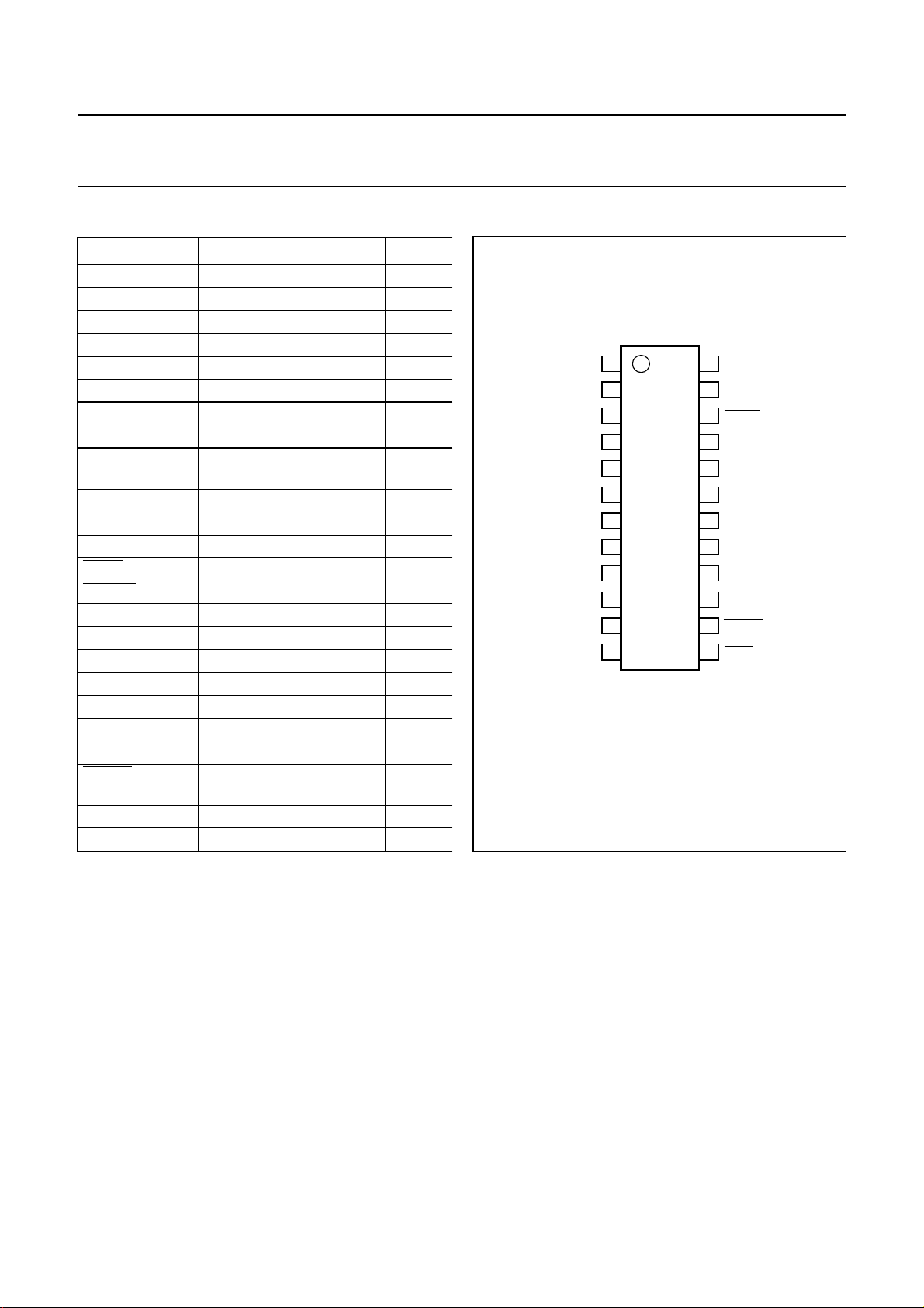
handbook, halfpage
WX
1
V
2
SS1
WY
3
WD
4
V
5
DD1
INA
6
7
8
9
10
11
12
TZA1000
MGG659
INB
ISENSE
V
DD3
SCLK
SDEN
SDIO
Fig.2 Pin configuration.
24
23
22
21
20
19
18
17
16
15
14
13
BIASA
BIASB
RESET
I
ref
V
ref
OUTA
OUTB
V
DD2
V
SS2
CLK
WGATE
HOLD
Notes
1. Pin type abbreviations: O = output, I = input,
P = power supply.
2. Digital inputs: LOW: <0.3V
; HIGH: >0.7VDD.
DD
3. Use only for connecting current reference resistor.
See Chapter “Equivalent pin circuits” for the I/O
configuration of the analog pins.
1998 Mar 17 5

Philips Semiconductors Preliminary specification
QIC read-write amplifier TZA1000
FUNCTIONAL DESCRIPTION
The preamplifier
The gain and dynamic range of the symmetrical low noise
preamplifier can be varied to accommodate a wide
variation in input signal amplitude (see Table 11).
The 40 dB and 34 dB gain settings are provided for normal
use. The 40 dB setting offers the lowest noise figure. The
4 dB gain setting is intended for IC testing only.
The servo preamplifier
This low noise preamplifier can be used for reading
signals, such as QIC 3095 (Travan 4) servo signals, via
the recording head write coil. Servo mode is selected
either by resetting bits AI0 and AI1 in the control register
(see Table 9) or by means of the
control bit must be set when HOLD goes LOW; see
Table 7). When servo mode is selected, the maximum
total gain is set automatically regardless of, and without
overwriting, gain settings. Fast switch-over from read
mode to servo mode can thus be achieved without having
to alter register values.
Variable gain stage and AGC
The input to the variable gain stage can be switched to the
preamplifier output, to the output of the bias/FB (Feed
Back) circuit, or to the servo preamplifier output. When
using magnetic feedback, the bias/FB circuit output should
be selected (see Table 9).
The AGC range is 15 dB. The gain is programmable in
1 dB steps (see Table 12). If the output signal is too small,
a digital control circuit will increase the gain from minimum
to maximum in approximately 10 ms. If the output signal is
too large, the gain will be reduced from maximum to
minimum in approximately 0.2 ms. These values assume
a 24 MHz clock frequency. The upper limit of the gain
control range can be extended by 6 dB by setting the
G6DB bit in the control register via the serial interface (see
Table 13).
HOLD pin (the HSM
The AGC will maintain outputs OUTA and OUTB at
1.1 V (p-p). Additional level adjustment points are
provided by the 34 or 40 dB preamplifier gain switch (see
Table 11) and the −10 or −4 dB bias output attenuation
switch (see Table 9).
High-pass filter
The HPF (High-Pass Filter) is used to differentiate
yoke-type head signals. It is followed by an additional gain
stage (21 dB). The HPF cut-off frequency is coupled to the
cut-off frequency of the LPF (Low-Pass Filter), and is
selectable in 4 steps: 1, 2, 4 and 10 MHz (see Table 2).
The HPF can be bypassed for SIG heads (see Table 8).
Low-pass filter
The second order low-pass filter is used to attenuate high
frequency noise above the signal bandwidth, mainly to
provide anti-aliasing filtering for the A/D converter in the
digital equalizer. The cut-off frequency of the LPF is
selectable in 4 steps: 1, 2, 4 and 10 MHz (see Table 2).
Sense current circuit
The sense current circuit is a programmable current
source, operating from the 12 V supply (V
programmed to supply a current between 0 and 15 mA,
with 7-bit resolution. The current range can be doubled,
then ranging from 0 to 30 mA, by setting the SDB bit in the
control register (see Table 15). The sense current circuit
can be disabled by resetting the ENS bit (see Table 4).
This is the only circuit on the IC that uses the 12 V supply.
The output must be decoupled with a low impedance
capacitor (10 µF recommended) to reduce noise coupling
into the head.
For the current source circuit to operate correctly, the
voltage difference between V
(pin 8) must be at least 1.6 V.
(pin 9) and ISENSE
DD3
). It can be
DD3
The AGC is frozen while the
TZA1000 is writing, or the IC is in servo mode.
The AGC can be operated internally, running on the CLK
clock signal on pin 15 (HOLD HIGH and GFXD LOW; see
Table 12), or externally by means of a software algorithm
(GFXD HIGH). When operated externally, either the DN bit
in the status read register (see Table 17) or the level
measurement in the digital equalizer IC (SZA1000) can be
used as input to the algorithm.
1998 Mar 17 6
HOLD input is LOW, the

Philips Semiconductors Preliminary specification
QIC read-write amplifier TZA1000
Bias and magnetic feedback circuit
This circuit can be used to generate AC and DC bias
currents (for a yoke-type MR head, for instance).
The DC bias output voltage is programmable
between 0 and 1.4 V, with 5-bit resolution (see Table 3).
The DC current generated is this voltage divided by the
total bias resistance (head coil + total series resistance).
The AC signal input to the circuit can be switched to the
preamplifier output (see Table 10). In this way, magnetic
feedback inside the head can be achieved. This limits
head distortion, and prevents head saturation from large
tape signals, like QIC 80 recordings.
The open loop gain of the feedback loop depends on head
sensitivity, the selected sense current (see Table 15), and
the selected preamplifier gain (see Table 11). The values
of the external resistors connected in series with the bias
conductor can be used to set the gain. For loop stability at
high frequencies, the bandwidth of the magnetic feedback
amplifier is limited to 5 MHz.
In closed loop mode, the effective cut-off frequency for the
playback signals will increase with the feedback factor. For
this reason the read signal can be taken from the output of
the bias circuit.
To prevent loop instability at low frequencies, the
preamplifier input capacitors should be chosen such that
the cut-off frequency at that point is well above, or well
below, the internal cut-off frequency of the AC coupling
between the preamplifier and the bias circuit (input
impedance of the preamplifier is typically 2 kΩ).
The maximum (peak AC) current that the bias circuit can
deliver can be adjusted to achieve an optimum balance
between required current range and power consumption
(see Table 3). The AC circuit is switched off when the
TZA1000 is writing, and the maximum current is switched
to 10 mA. This limits power dissipation during writing.
Test generator
1
This circuit generates a test signal with a frequency
⁄
16
that of the signal at the CLK input (pin 15). By switching the
AC input of the bias circuit to the internal test generator
(see Table 10), the read channel can be tested.
The differential output value is typically 100 mV (p-p).
This facility can also be used to adjust the DC bias voltage
while monitoring the signal at the read element in the head.
The optimum DC bias level setting is just before the output
from the read head reaches its peak.
Write circuit
The write circuit is a differential current source that can
generate a near rail-to-rail output voltage to get the
shortest current transition time. Writing is enabled when
WGATE is LOW. The polarity of the current depends on
the WD input pin. The WDM bit in the control register
determines the write signal mode: WD (Non-Return to
Zero) or WDI (Return to Zero; see Table 14). When WDI
mode is selected, the polarity of the write current is
reversed at every falling edge of the WD input. When WD
mode is selected, the polarity of the write current is
reversed when the polarity of WD changes. The write
current is programmable between 0 and 125 mA, with
7-bit resolution (see Table 14).
The IC is specified for a write current of up to 100 mA.
Overshoot caused by an inductive load can be minimized
by means of a single external resister local to the IC.
Write unsafe detector
The write unsafe detector will detect an open write coil, or
one shorted to ground. The circuit is enabled only while the
TZA1000 is writing. A resistance to GND or V
of less
DD
than 10 Ω, or a series resistance greater that about 300 Ω,
will be detected (these values are write-current
dependant). If an error occurs, the WUS status bit is set.
This bit can be read via the serial interface. The WUS bit
will remain set until the status byte is read.
Power fail detector
The power fail detector will detect a low voltage on the 5 V
(V
) or 12 V (V
DD1
3.75 V for V
DD1
) supply lines. The thresholds are
DD3
and 9 V for V
. A power failure is
DD3
detected if the voltage is below the threshold for 1 µs or
longer. If a 5 V power failure occurs, the status bit PF5 is
set. If a 12 V power failure occurs, the status bit PF12 is
set. These bits can be read via the serial interface, and will
remain HIGH until the status byte is read.
When a 5 V power failure occurs, the RESET output goes
LOW and the write circuit is disabled (in addition to PF5
being set). The RESET output has an internal 18 kΩ pull
down resistor to guarantee a LOW level at the output even
when a power failure occurs. During normal operation, the
RESET pin should not be held LOW by an external circuit,
since this will switch the IC into test mode.
1998 Mar 17 7

Philips Semiconductors Preliminary specification
QIC read-write amplifier TZA1000
DACs
There are 3 internal DACs:
1. The Sense DAC: current DAC; 7-bit resolution
2. The Write DAC: current DAC; 7-bit resolution
3. The Bias DAC: voltage DAC; 5-bit resolution.
The Sense and Write DAC current settings are a function
of the reference current I
(at the I
ref
pin). I
ref
is multiplied
ref
by a 7-bit factor: S0 to S6 for the sense DAC, W0 to W6 for
the write DAC (see Tables 14 and 15). If the resistance
between I
and GND is increased (or decreased), the
ref
DAC output currents will be decreased (or increased) by
the same factor. In this way, the DAC output current
ranges can be adjusted.
The current values specified, and the equations used to
calculate Sense and Write currents (see Tables 14
and 15), are for a 430 Ω resistance between I
and GND.
ref
This resistance can be varied between 250 Ω and 1 kΩ,
giving a ±2 × DAC modification range. For reasons of
noise and stability, the voltage at the I
pin should not be
ref
used in any other part of the circuit.
Clock handling
The TZA1000 has 2 clock inputs:
CLK: the general clock input, pin 15
SCLK: the serial interface clock input, pin 10.
CLK is used for status register read and write cycle timing
and for operating the internal AGC. When the AGC is not
being used and serial communications are not active, CLK
may be switched off. This can help reduce crosstalk on the
printed circuit board.
When accessing the status register, the CLK frequency
must be at least 16 × SCLK frequency. It is recommended
that the 24 MHz clock supplied by the SZA1000 be used
directly.
Serial interface
The 3 wire serial interface recognizes 8-bit addresses and
8-bit data. To read data from the status register, hex
address FF must be transmitted. The IC will then respond
with the contents of the 8-bit status register.
1998 Mar 17 8
 Loading...