

Page 1
Colour Television Chassis
CL 965320690-164.eps
020999
FTV1.9EE
AA
Contents Page
1 Introduction
2 Mechanical instructions
3. Blockdiagram
4Service modes
5Audio
6Video
7 Control
8 Featurebox
9 Double window
10 Teletext
11 Audio Video buffer
12 Front I/O panel
13 Power supply
14 Switch panel
15 LED panel
2
5
9
10
22
31
46
49
58
63
64
71
73
79
80
©
Copyright reserved 1999 Philips Consumer Electronics B.V. Eindhoven, The
Netherlands. All rights reserved. No part of this publication may be reproduced,
stored in a retrieval system or transmitted, in any form or by any means, electronic,
mechanical, photocopying, or otherwise without the prior permission of Philips.
Published by JvR 9969 Service PaCE Printed in The Netherlands Subject to modification 5 3122 785 10033
Page 2
2 1. Introduction FTV1.9EE Receiver Box
1. Introduction
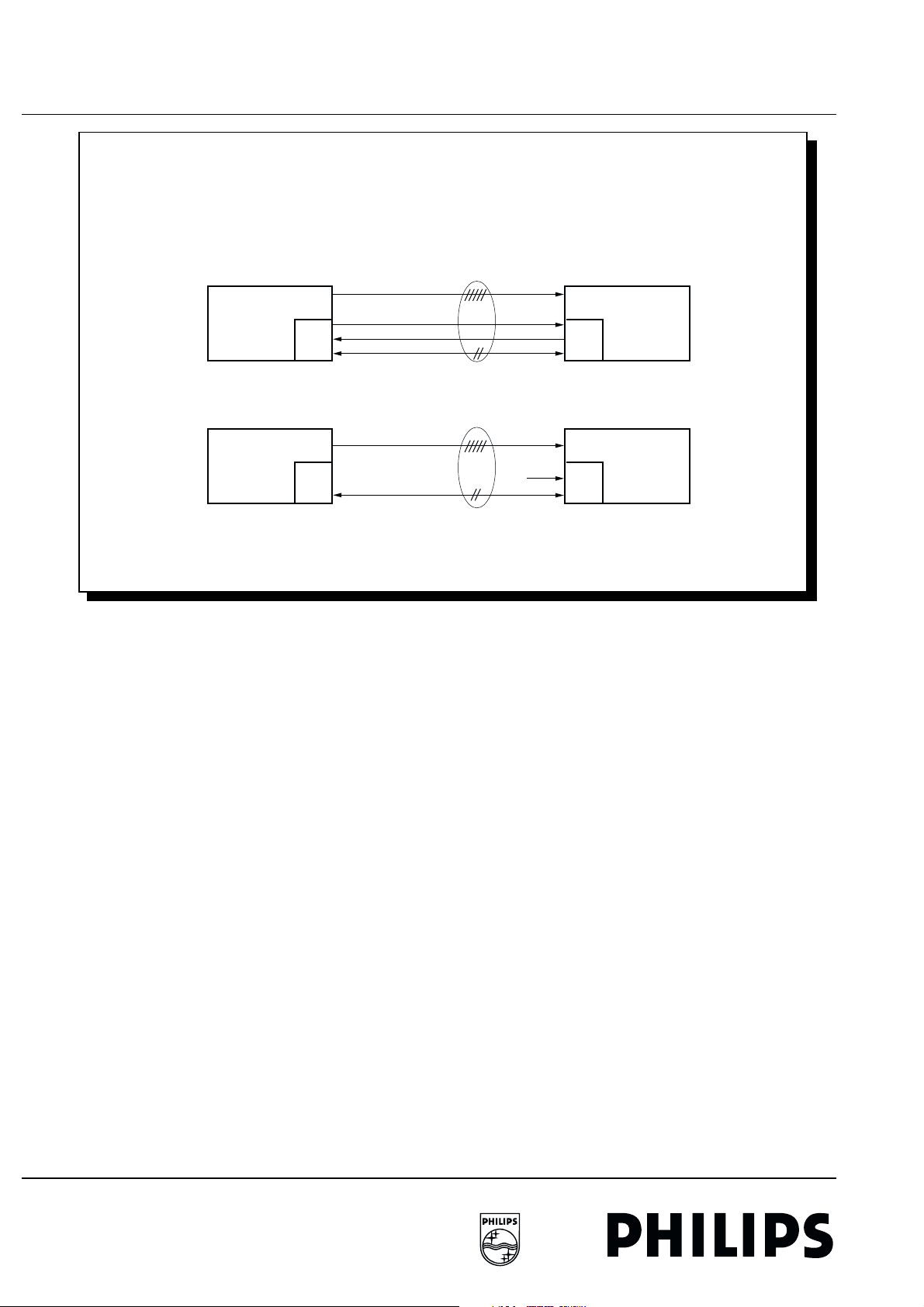
CONFIGURATIONS
TV-CONFIGURATION
R, G, B, HS, VS
RECEIVER BOX
µP µP
MONITOR-CONFIGURATION
PERSONAL COMPUTER
µP µP
CONFIG_IDENT
DIS_RC_5
UART
R, G, B, H, V
CONFIG_IDENT
DDC
DISPLAY BOX
DISPLAY BOX
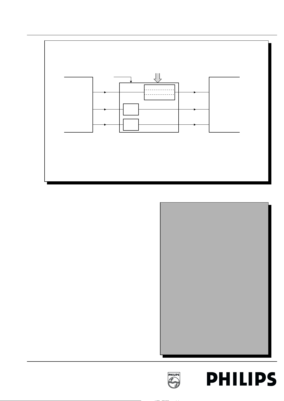
The FTV1.9 is the successor of the FTV1.5, which had to be
cheaper than the FTV1.5 with as much as possible "re-use" of
the FTV1.5.
In this set, as in the FTV1.5, the Small Signal Panel (SSP) of
the GFL is used.
The Flat TV 1.9 is built around the E-Box (= Receiver Box) and
the 42" Monitor (= Display Box).
Within the Monitor a Fujitsu Plasma Display Panel, version 5, is
used.
For the FTV1.9, the E-box is used in the TV-configuration only
(Monitor connected to the E-box).
The FTV1.9 family has been set up for Europe, USA, Asian and
LATAM markets.
The Europe type (FTR9952) consists of 2 Versions:
• FTV1.9 Western Europe stroke /12
• FTV1.9 France/UK stroke /19
The E-Box and the Monitor are separate devices, which can
also be sold and serviced separately.
The E-box, can be serviced by using a test pattern coming from
the FBX inside the E-box or via a PC/laptop by using ComPair
via the bi-directional LED at the front.
The Display-box or a PC-monitor is used only as a display.
In case the E-box goes into protection, there is the possibility to
read out the content of the error code buffer by means of the:
• DST : Transmit the command:
"DIAGNOSE - x - OK" which gives you the error-code of the
error buffer at position x
CL 96532069_002.eps
240899
The E-Box is based on the electronic box of the FTV1.5,
however several parts have been adapted.
• Two panels have been moved to the Monitor:
– Audio amplifier.
– Monitor supply; Preconditioner and VsVa supply.
• The Dolby processing has been deleted.
• The small signal electronics is "taken over from/based
upon" the GFL.
Existing small signal parts have been adapted and new small
signal parts have been developed.
• Development of 2 new panels to optimise interfacing with
the monitor:
– AV buffer.
– E-box supply.
• Development of several new panels to adapt to the
mechanical design of the FTV1.9:
– Front I/O panel.
– LED panel.
– Switch panel.
Page 3
FTV1.9EE Receiver Box 1. Introduction 3
1.1 Short description of the main functional parts.
1.1 Short description of the main functio nal part s.
• Mains cord (detachable).
• Antenna cable.
– Ferrite's added to reduce the radiation.
• Switch panel E-box (FL).
• Led panel E-box (LE).
– Red and Green indication controlled by the µP.
• AV Buffer (AVB).The function of this panel is to interface the
signals between the panels inside the Receiver box, and to
interface the Receiver- with the Display box via a VGA
cable.
– Control / RC5.
– RGB selection.
– Sandcastle generator.
– Audio select.
– YUV to YC decoder.
– VGA_in and VGA_out connector.
• E-Box supply (SU).
– Small signal set supply (5V, 8V6, 12V, 40V) and
Standby supply (+5V_STBY).
• Front panel box (AV).
– Front I/O's (Y/C Hosiden & CVBS CINCH video inputs,
L/R CINCH audio inputs, headphone output, IR
transmitter LED for Service Dealer Tool, IR receiver for
RC5).
• Small signal panel (S).
– Front end (S1).
– Stereo Decoder (S2).
– Sound processing (S3).
– Headphone amplifier (S4).
– Video processing (S5).
– Video control (S6).
– Control (S8).
• Incredible Sound (AY). The incredible sound circuit
electronically generates a phase and sound level relation
between the left and right signal, in such a way that to the
human mind it sound as if the sound is actually coming from
the far left or right side.
• Euro I/O (I).
– SCART I/O's.
– CINCH audio output.
– video and audio matrices for source selection.
• Eco NICAM (G).
– audio (NICAM) decoding.
• Double window module (P).
– Combination of 2 video signals to DW, or Multi PIP.
– Tuner, IF and video processor for the sub channel.
• Feature box (FBX).
– Digital scan for 50 Hz systems (PAL/SECAM).
– Multi PIP processing.
– Vertical and horizontal zoom functions.
– Line flicker reduction.
Personal notes
Page 4
4 1. Introduction FTV1.9EE Receiver Box
1.2 Audio/Video Diversity
1.2 Audio/Video Diversity
• Western-Europe /12: FQ916ME.
• France/UK /19: FQ916DMF.
Personal notes
Page 5
FTV1.9EE Receiver Box 2. Mechanical instructions 5
CL96532069_133.EPS
030899
CL96532069_124.EPS
090899
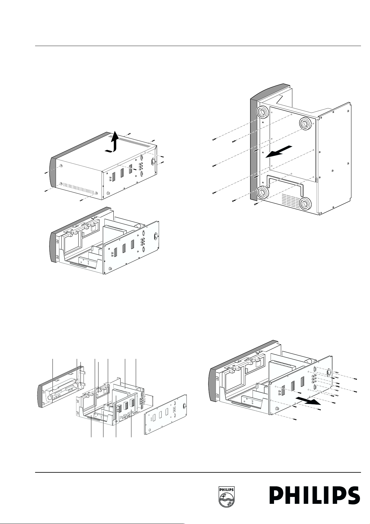
2.1 Introduction:
2. Mechanical instruction s2.1Introduction:
There are pre-defined service positions for the following panels:
1. SSP (copper side).
2. EURO/IO panel.
3. TXT panel.
4. FRONT/IO panel.
5. SUPPLY panel.
6. AV BUFFER panel.
7. NICAM panel.
8. FEATURE BOX panel.
9. DOUBLE WINDOW panel.
1. All panels are now accessible (except for the SSP).
SMALL SIGNAL panel (SSP).
CL96532069_121.EPS
110899
Figure 2-1
Before these panels can be accessed, the top cover has to be
removed:
1. For safety reasons first unplug the Mains cable.
1. Remove the 8 fixation screws of the top cover: 2 x 3 at the
sides, 2 at the rear.
2. Remove the top cover (during removal push it slightly
backwards).
Front endFront I/O LED AV-Buffer Supply
Switch TXT
Double Window
Figure 2-3
1. Place Receiver Box on its side.
2. Remove the 8 fixation screws of the bottom cover.
3. The copper side of the SSP becomes accessible. Here the
I/O's of the several modules easily can be checked. For the
FEATURE BOX (FB) and the DOUBLE WINDOW (DW)
panel this must be the information to decide to order a new
panel.
4. For the NICAM panel it can give some information whether
this panel is malfunctioning.
EURO/IO panel.
EURO I/OFeature BoxNICAMSSP
Figure 2-2
CL96532069_122.EPS
090899
Figure 2-4
1. Remove the metal rear cover by unscrewing in total 15
screws: 6 at the rim, 3 at the EURO/IO panel and 6 at the
sub_D and CINCH connectors.
Page 6
6 2. Mechanical instructions FTV1.9EE Receiver Box
Supply
2.1 Introduction:
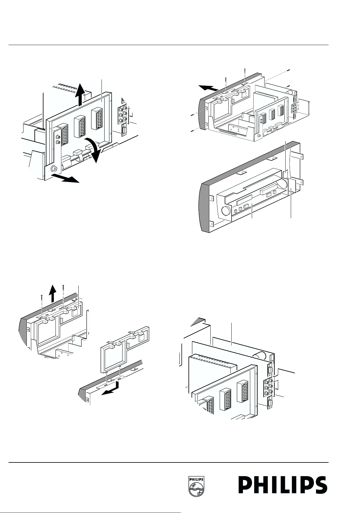
2. Now the EURO/IO panel becomes accessible at the
component side.
EURO I/O
2
3
1
Figure 2-5
1. Remove the copper shielding from the antenna-input
connector [1].
2. After lifting the bracket from the SSP [2], it can be rotated in
such a way that also the copperside becomes available [3]
(bracket can also be removed completely if necessary).
CL96532069_125.EPS
090899
FRONT/IO panel.
Front I/O Switch
Figure 2-7
LED
CL96532069_127.EPS
090899
TELETEXT panel (TXT).
TXT
1
2
CL96532069_126.EPS
090899
Figure 2-6
1. Remove the 2 fixation screws at the top of the bracket [1].
2. Bracket (with panel) can now lifted and placed upon the
front metal wall [2].
1. First remove the front cover: 2 x 2 screws at the sides and
2 at the top.
2. FRONT I/O, LED and SWITCH panels now can be serviced.
SUPPLY panel.
CL96532069_128.EPS
Figure 2-8
090899
Page 7
FTV1.9EE Receiver Box 2. Mechanical instructions 7
AV-Buffer
2.1 Introduction:
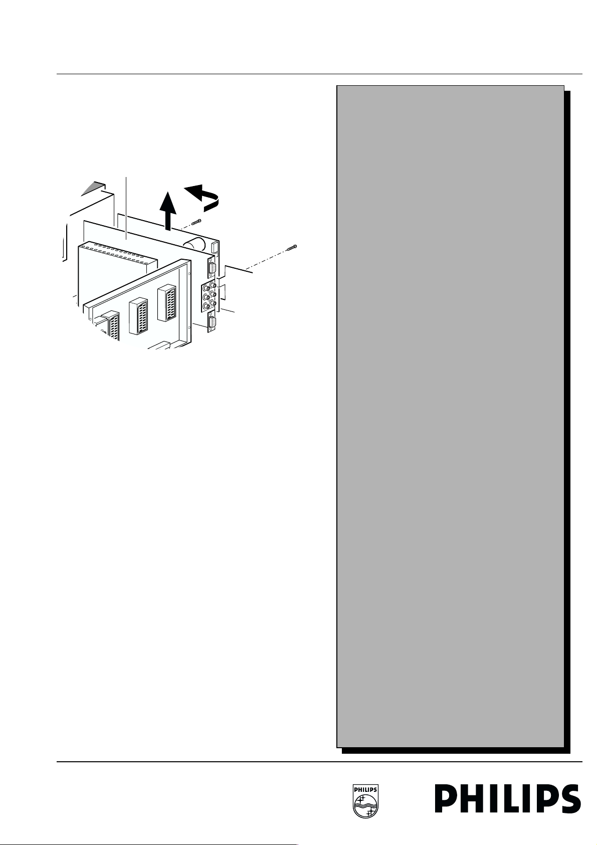
The copper side of this panel is fully accessible at the outer side
of the Receiver Box. Be aware that the mains voltage is always
present on this board, even if the mains switch is OFF !
AUDIO VIDEO BUFFER panel.
Personal notes
2
3
1
1
CL96532069_129.EPS
Figure 2-9
1. First remove the adjacent SUPPLY panel. This can be done
by removing the 2 fixation screws [1] and lifting this panel
from its bracket [2]. Rotate this panel in such a way that the
copper side is positioned (in an electrical safe way) aside of
the Receiver Box [3].
2. Now the copper side (SMD or A-side) of the AV-BUFFER
panel becomes accessible. All service test points are
positioned on this A-side.
090899
NICAM panel.
This panel can be checked via the I/O connector on the SSP.
For service properties (exchanging parts) see chapter 2.2.
FEATURE BOX.
This panel can be checked via the I/O connector on the SSP.
For service properties (exchanging parts) see chapter 2.2.
DOUBLE WINDOW panel.
This panel can be checked via the I/O connector on the SSP.
For service properties (exchanging parts) see chapter 2.2.
Page 8
8 2. Mechanical instructions FTV1.9EE Receiver Box
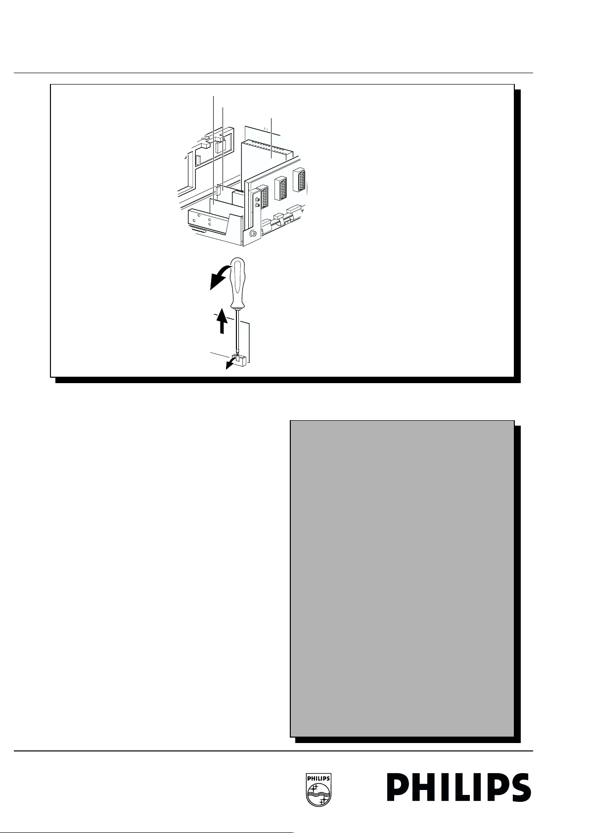
2.2 Exchanging parts
2.2 Exchanging parts
NICAM
Double Window
1
2
1
Feature Box
CL96532069_123.EPS
110899
Some parts of the FTV1.9 Receiver Box must be exchanged if
defective:
• DOUBLE WINDOW panel.
• FEATURE BOX.
All these panels can be lifted from the SSP by releasing the 2
connector slots sidewards while lifting.
Personal notes
Page 9
FTV1.9EE Receiver Box 3. Block diagram 9
2.2 Exchanging parts
3. Block diagram
For the block diagram see Service Manual Chapter 6.
The power is supplied by the E-box supply (Flyback converter).
The mains input voltage has a range between 95 and 264 VAC
The output voltages are:
• 33 V
• 12.8 V
•8.6 V
•5.1 V
• 5 VSTNBY
• POR -signal (reset-pulse for the µP)
The controls located on the SSP panel, are activated by RC5
signals from the remote control receiver on the LED panel Ebox.
Several external sources can be connected to the E-box via:
• 3 SCART inputs at the Euro I/O.
• Several connections at the front (CVBS, YC, Headphones
and audio-CINCH'es).
• VGA input connector at the AV Buffer panel.
The Tuner is suitable for the reception of VHF1, VHF3, UHF, Schannels and Hyperband. The output supplies the CVBS
picture and a mono or stereo audio signal. The following Tuner
types are used within the E-box :
• FQ 916 DME/PH MK2 BG/L/M used in the Western Europe
set /12
• FQ 916 DMF/PH MK2 BG/L/L'/I used in the France/UK set
/19.
The NICAM module (G) has been added to demodulated the
SIF - NICAM signals.
The Audio signals coming from the front I/O panel are
processed by IC7650 (TDA9860) and are passed through to
selector IC7901 (TEA6422). This IC switches the processed
audio signals or the audio signals coming from the VGA_input
connector to the output CINCH for the monitor.
The video signal coming from the Front I/O panel or tuneroutput are first passed through a COMB filter before they are
processed by the Video Control IC7352 (TDA9114).
The YUV output signal and the sync-signal H/V are transferred
to the DW panel.
On the DW-panel there is another tuner-section: UV12160. The
output signal from the DW-tuner is processed by the PIPO
(Picture In Picture Out) processor SAA9077.
The output of the TDA8601 is offered to the FBX4 to convert the
signals to 2fh and to process features like natural motion; DNR
etc.
On the SSP panel the YUV signals are converted into RGB
signal by Video Control IC7500. OSD info (Teletext) is added,
before the signals are send to the AV Buffer panel. Selector
IC7600 switches these RGB-signals or the RGB-signals
coming from the VGA_in connector to the VGA-out connector.
Personal notes
Page 10
10 4. Service modes FTV1.9EE Receiver Box
4.1 Introduction
4. Service modes4.1Introduc tion
The E-Box and the Monitor are separate devices, which can
also be sold and serviced separately.
The E-box, as a stand-alone unit, can be serviced by using a
test pattern coming from the FBX inside the E-box or via a PC/
Laptop by using ComPair via the bi-directional LED at the front.
The Europe type (FTR9952) consisting of 2 Versions:
• FTV1.9 Western Europe stroke /12
• FTV1.9 France/UK stroke /19
In this chapter the following paragraphs are included:
1. Introduction
2. Test points
3. Dealer Service Tool (DST)
4. Service Modes
5. Error code buffer and error codes
6. Options in the Service Alignment Mode
7. Protections
8. Electrical alignments
9. Software alignments
The “Blinking Led” procedure
This procedure is not applicable on the "TV Configuration" of
the FTV1.9. It is only valid for the "Monitor Only Configuration"
(see SM Display Box).
Personal notes
Page 11
FTV1.9EE Receiver Box 4. Service modes 11
4.2 Test points
4.2 Test points
The FTV1.9 chassis is equipped with test points in the service
printing. These test points are referring to the functional blocks:
• B1-B2-B3, etc.: Test points for the AV Buffer
circuit (AVB)
• TP1-TP2-TP3, etc.: Test points for the Feature Box (F)
• S1-S2-S3, etc.: Test points for the Double window
(P) and the Small Signal Panel SSP (S1-S8)
• P1-P2-P3, etc: Test points for the Supply E-box
(SU)
Measurements are performed under the following conditions:
Video: colour bar signal; Audio: 3 kHz left, 1 kHz right
Personal notes
Page 12
12 4. Service modes FTV1.9EE Receiver Box
4.3 Dealer Service Tool (DST)
4.3 Dealer Service Tool (DST)
For easy installation and diagnosis the dealer service tool
(DST) RC7150 can be used. When there is no picture (to
access the error code buffer via the OSD), DST can display the
contents of the entire error code buffer, via the send-LED, on its
own LC display. The ordering number of the DST (RC7150) is
4822 218 21232.
Installation features for the dealer
The dealer can use the RC7150 for programming the TV-set
with pre-sets. 10 Different program tables can be programmed
into the DST via a GFL TV-set (downloading from the GFL to
the DST; see GFL service manuals) or by the DST-I (DST
interface; ordering code 4822 218 21277). For explanation of
the installation features of the DST, the directions for use of the
DST are recommended (For the FTV1.9 chassis, download
code 4 should be used).
Diagnose features for service
FTV1.9 sets can be put in two service modes via the RC7150.
These are the Service Default Mode (SDM) and the Service
Alignment Mode (SAM).
Personal notes
Page 13
FTV1.9EE Receiver Box 4. Service modes 13
4.4 Service Modes
4.4 Service Modes
Below described sequence is only valid for the "TV
Configuration", when a Monitor is connected to an E-box. When
you have to service the "Monitor Only Configuration" , please
check chapter 5 in the Training Manual of the Display Box.
Service Default Mode (SDM)
The purpose of the SDM is:
• provide a situation with predefined settings to get the same
measurements as in this manual.
• Inspect the error buffer.
• Possibility to overrule software protections via the service
pins (caution: override of software protections! ).
Entering the SDM:
• By transmitting the "DEFAULT" command with the RC7150
Dealer Service Tool (this works both while the set is in
normal operation mode or in the SAM).
• When using a standard RC: sequence 062596 followed by
the "MENU" key.
• By short-circuiting the SDM pin on the SSP panel (see TM
Receiver Box chapter 4).
Exit the SDM:
Switch the set to Standby.
Note: When the mains power is switched off while the set is in
SDM, the set will switch to SDM immediately when the mains is
switched on again. (The error buffer will not be cleared).
The SDM sets the following pre-defined conditions:
• Volume level is set to 25% (of the maximum volume level).
• Linear Audio and Video settings are set to 50%.
• Colour temperature is set to normal.
The following functions are "overruled" in SDM since they
interfere with diagnosing/repairing a set
• Video blanking.
• Slow demute.
• Anti-ageing.
• Automatic switch to "Standby" when H- and/or V-sync
signals are lost.
All other controls operate normally.
Special SDM functions
Access to normal user menu:
Pressing the "MENU" button on the remote control will enter the
normal user menu (TV lock, Installation, Brightness, colour and
contrast) while "SER" remains displayed in top of screen).
Pressing the "MENU" key again will return to the last SDM
status.
OSD:
Pressing the "OSD" button on the remote control shows all
OSD information (incl. error buffer).
Service Alignment Mode (SAM)
The purpose of the SAM is to align and or adjust settings.
Entering the SAM-menu:
• By pressing the "ALIGN" button command on the RC7150
DST followed by code 3140 and "OK". Note: when pressing
the "ALIGN" button, point to the IR-receiver of the Display
Box but after that (for entering the code, etc.), point to the
IR-receiver of the Receiver Box!
• Standard RC sequence 062596 followed by the key "OSD".
• By short-circuiting the SDM pin (connector S98) on the SSP
panel (caution: override of software protections! ).
Exit the SAM:
Push the "STANDBY" button on the Remote Control.
Note: When the mains power is switched OFF while the set is
in SAM, the set will switch to SAM immediately when the mains
is switched ON again. (The error buffer will not be cleared).
In the SAM the following information is displayed on the screen:
--------------------------------------------------
E-box
Date : Id: (1)
Operation hours : (2)
Errors (3)
Defect. Modules : (4)
Reset Error Buffer (5)
Functional Test E-box (6)
Alignments E-box (7)
Display Info D-box (8)
--------------------------------------------------
Explanation notes/references:
(1) Date : dd-mm-yy
Software identification of the main micro controller (F19EBC
X.Y_#####)
• F19E is the chassis name for FTV1.9 E-box
• B is the region identification
• C is the language cluster
• X = (main version number)
• Y = (subversion number)
• ##### are the last 5 digits of the 12nc number
(2) Operation hours: Normal display operation in hours
(resolution 0.5 hrs)
(3) Errors: The contents of the error buffer (max. 10 errors)
displayed on 2 lines. The last error that occurred is displayed
at the most left position. When the errorlist is empty " No errors"
is displayed.
(4) Defect. Module: The defective module, associated with a
nr. according to the following table:
Nr Module-name Diagram
1 Control S8 - Main processor 7200
2 Frontend S1 - Main tuner 1300
3 Source Select Europe I2 - Audio selector 7822
4 Video Processing (SSP) S5 - 7352
5 Video controller S6 - 7580
7 2CS decoder S2 - 7600
8 Nicam decoder G - 7501
9 Audio control S3 - 7650
12 Teletext AQ - 7451
13 Feature box F - micro-processor 7505
14 16:9 processor P - 7860
16 Source Select Global I1 - Video selector 7823
17 Global Sound Decoder G - Multi FM selection 7630
20 Double Window P 21 BTSC Decoder G- 7550
22 Closed Caption (USA) BC
Page 14
14 4. Service modes FTV1.9EE Receiver Box
4.4 Service Modes
Nr Module-name Diagram
23 HD Module (USA) AO
56 AV Buffer AVB1 or AVB4
Exceptions:
– No errors then "None" is displayed
– Errors caused by more than 1 module then "Unknown" is
displayed
– Display of "SW protection" or "HW protection" if only this
error is reported otherwise display of the defective module
according the list.
(5) Reset error buffer E-box
(6) Functional test E-box: All IC devices are checked. No
acknowledge results in a particular device error report.
(7) Alignments E-box: Menu control
(8) Display Info D-box: Display service data (Menu control)
This is the main menu of the Service Alignment Mode screens,
which has the following structure:
Alignments E-box
The Service Alignment menu has the following items :
• General, see 'General menu control' below.
• Options, see 'Options menu control' below.
• Option number, see 'Option number menu control' below.
•Store.
General Menu Control
The General Menu has another 7 menu-items of which White
Drive and Luminance Delay have several sub-items.
•White Drive
– Testpattern : ON/OFF
–Red
– Green
–Blue
• Adjust Peak White Limiter
• Input level Stereo Decoder
• Stereo Channel Separation
• Luminance Delays
– Lum. Delay PAL
– Lum. Delay SECAM
– Lum. Delay NTSC
• FBX Test Pattern : ON/OFF
• Contrast
Options Menu Control
The Options Menu has another 7 menu-items of which 5 items
have several sub-items.
•TV Systems
– FV916MG
–FQ916MR
– FQ916(D)MF
– FQ916(D)ME
–FQ936D
–FQ944D
– Chinese Tuners
–FS988
• Stereo Decoder
– NICAM type [selection ]
– Not available
–BG or I
–BG + I
– Eco NICAM
– 2 CS [Yes/No ]
– Global [Yes/No ]
• Double Window
– DW Available [ Yes/No ]
– Mosaic [Yes/No ]
• Video Repro
– Combfilter [ Selection ]
– Not Present
– SAA4961
– Dynamic Contrast [ Yes/No ]
– Digital Panorama [ Yes/No ]
– Auto Format FBX [Yes/No ]
• Source Select
– SS type [ Selection ]
– Europe
– Global
• Teletext
– TXT [Yes/No]
– PDC/VPS [Yes/No]
– TXT Pre-set Table [Yes/No]
• Easy link [Yes/No ]
Option number Menu control
The Options Number Menu has another 2 menu-items of which
both items have several sub-items.
• HW Opt Nr : 4 numbers of 5 digits
• SW Opt Nr : 2 numbers of 5 digits
The table below contains the default values of the HW and SW
option numbers.
Destination PAL+
Europe No 01024-1
" Yes 01024-1
France No 01025-1
" Yes 01025-1
HW Option
number
14353-2
10624-3
16452-4
14353-2
14592-3
16452-4
14353-2
10624-3
16452-4
14353-2
14592-3
16452-4
SW Option
Number
00000-1
04884-2
00000
04884
00000
04884
00000
04884
Store
Stores the changed item(s) in the NVM.
Display Info D-box
In this screen the menu of the monitor is displayed on the PDP:
--------------------------------------------------
Id: F19DE11.0_12345 (1)
Operation Hours: LLLLL (2)
Page 15

FTV1.9EE Receiver Box 4. Service modes 15
4.4 Service Modes
Errors: 14 08 02
-------------------------------------------------Software identification of the main micro controller (F19DBC
X.Y_#####)
• F19D is the chassis name for FTV1.9 Display
• B is the region identification
• C is the language cluster
• X = main version number
• Y = subversion number
• ##### are 5 digits of the serial numberr
(2) Operation hours: Normal display operation in hours
(resolution 1 hrs)
(3) Errors: The contents of the error buffer (max. 10 errors).
The last error that occurred is displayed at the most left
position. When the errorlist is empty "No errors" is displayed.
Access to normal user menu:
Pressing the "MENU" button on the remote control will enter the
normal user menu (TV lock, Installation, Brightness, colour and
contrast) while "SAM" remains displayed in top of screen.
Pressing the "MENU" key again will return to the last SAM
status.
OSD:
Pressing the "OSD" button on the remote control shows all
OSD information (incl. error buffer).
Access to SDM:
Pressing the "DEFAULT" button on the DST
SAM menu control:
Menu items can be selected with the "UP" or "DOWN" key.
Entry into the selected items (sub menus) is done by the "LEFT"
or "RIGHT" key. The selected item will be highlighted.
With the same "LEFT/RIGHT" keys, it is possible to increase/
decrease the value of the selected item.
Return to the former screen by pushing the "MENU" button. The
item values are stored in NVM if the sub menu is left.
Customer Service Mode
FTV1.9 sets are equipped with the "Customer Service Mode"
(CSM). CSM is a special service mode that can be activated
and de-activated by the customer, upon request of the service
technician/dealer during a telephone conversation in order to
identify the status of the set. This CSM is a 'read only' mode,
therefore modifications in this mode are not possible.
Entering the Customer Service Mode:
• By pressing simultaneously the "LOCAL MENU" button on
the local keyboard and the button (Mute) on the RC.
Exit of the Customer Service Mode:
• pressing any key on the remote control handset (except
"P+" or "P-")
• switching off the TV set with the mains switch.
The screen has the following set-up:
--------------------------------------------------
CUSTOMER SERVICE MENU 1
1. SW Ver.
2. Code 1
3. Code 2
4. PP Volume
5. PP Colour
6. PP Brightness
7. PP Contrast
8. PP Headphone volume
9. Sharpness
10. Child lock
11. External Center Sound
-------------------------------------------------Pressing the "P+" button on the RC shows page 2 of the CSM.
Pressing "P-" shows again page 1 of the CSM.
-------------------------------------------------CUSTOMER SERVICE MENU 2
1. Incredible Sound
2. DNR
3. Noise Figure
4. Colour System
5. TV System
6. Audio System
7. Tuned bit
8. DVD/Photo CD
9. Sleep Timer
10. On Timer
-------------------------------------------------Display in the [MenuItems] field:
1. Software Identification: AAA=Chassis name, BB=Function
name, C=Language cluster, X=main version nr. Y=sub
version nr.
2. The last 5 error nr's in the error buffer(This line will be empty
when there are no errors)
3. The first 5 error nr's in the error buffer.(This line will be
empty when there are no errors)
4. Personal preference value of the volume
5. Personal preference value of the colour
6. Personal preference value of the brightness
7. Personal preference value of the contrast
8. Personal preference value of the headphone volume
9. Sharpness level
10. Child Lock status On/Off indication
11. Dolby Center Sound status On/Off indication
12. Incredible Sound status On/Off indication
13. DNR status
14. Indication of the signal quality
15. Colour System of selected program: PAL, SECAM or NTSC
16. Video system of selected program: BG, DK, I, L, M38.9 or
MN
17. Audio system of selected program: Sound Muted, Mono,
Stereo, Dual I, Dual II, Digital Mono, Digital Stereo, Digital
Dual I, Digital Dual II
18. Indication of whether the selected program is Tuned or not
19. Indication for whether or not DVD/Photo CD id selected
20. Only if the [value] of [SleepTimer] is NOT "0"
21. Only if the [starttime] of [OnTimer] is defined
Page 16
16 4. Service modes FTV1.9EE Receiver Box
4.5 Error code buffer and error-codes
4.5 Error code buffer and error-codes
The error code buffer contains all errors detected since the last
time the buffer was erased. The buffer is written from left to
right.
In case of non-intermittent faults, clear the error buffer before
starting the repair to prevent that "old" error codes are present.
If possible, check the entire content of the error buffers. In some
situations an error code is only the RESULT of another error
code (and not the actual cause).
Note: a fault in the protection detection circuitry can also lead to
a protection
The error code buffer will be cleared in the following cases:
• exiting SDM or SAM with the "Standby" command on the
remote control
• transmitting the commands "DIAGNOSE-9-9-OK" with the
DST.
The error buffer is not reset by leaving SDM or SAM with the
mains switch.
Examples:
ERROR: 0 0 0 0 0 : No errors detected
ERROR: 6 0 0 0 0 : Error code 6 is the last and only detected
error
ERROR: 5 6 0 0 0 : Error code 6 was first detected and error
code 5 is the last detected (newest) error
Error code Description Others
51 I2c slow bus error I2C slow bus
64 LTP (SSP) TDA9177
91 Data Receive Error
between Monitor and
E-box
92 Audio Source selector
(AV buffer)
93 I/O expander (AV
buffer)
Special
TEA6422
PCF8574AP
Error code Description Others
04 Non Volatile Memory 24C16
06 IF (SSP) FQ916ME
10 / 11 Audio matrix (Eco
Euro I/O)
13 Toshiba mP (Eco Euro
I/O)
15 Video processor
(XX44=Palplus) (SSP)
16 Video controller (SSP) TDA4780
19 2CS Stereo Decoder
(SSP)
20 3D eco Nicam
demodulator/decoder
21 / 22 Sound processor L &
R (SSP for non-Dolby
version)
28 IVT3 (TXT panel) SAA5270
29 FBX processor (FBX4) 87C654
34 Tuner (Double
Window)
37 Double Window SAB9077
38 I/O expander (Double
window)
39 Video processor
(Double Window)
44 5V supply error 5V supply
45 8V supply error 8V supply
49 Video matrix (Eco
Euro I/O)
TEA6430
TMP47C443N
TDA9144/43
TDA9840
3D SAA7282
TDA9860
UV1216E
PCF8574A
TDA9143
TEA6417
Personal notes
Page 17
FTV1.9EE Receiver Box 4. Service modes 17
4.6 Options in the “Service Alignment Mode”
4.6 Option s in the “Service Alignment Mode”
CurrentServi
ceSettings Options (NVM)
menus attributes Values associated
Service
Options Menu
Video
Reproductions
TVSystem
Options Menu
Stereo
Decoder
Options Menu
DW Options
Menu
Source Select
Options Menu
Service
Number Menu
easylink yes, no easylink = on, off
combfilter not present, combfilter = on, off
SAA4961
palplus_present yes, no palplus = on, off
frontend type FV916MG frontend =
FQ916MR = FQ916MR
FQ916(D)MF = FQ916(D)MF
FQ916(D)ME = FQ916(D)ME
FQ936D = FQ936D
FQ944D = FQ944D
Chinese Tuner = FQchina
FS988 = FS988
nicam_type not available,
2 CS yes, no twochannel = on,
Global yes, no soundexpander =
dwavailable yes, no dwavailable = on,
multipip yes, no multipip = on, off
sstype Euro sourceselect =
picturemute yes, no picturemute = on,
standby_on_tog
gle
virgin yes, no virgin = on, off
wss yes, no wss = on, off
vip_ltp_present yes, no vip_ltp = on, off
pipavail yes,no pip = on, off
txt_region west, east txtregion = west,
as_txt_preset_ta
ble
BG or I, BG + I ,
Eco Nicam
Global = global
yes, no standbytoggle =
yes, no aci = on, off
attributes of
Options
FV916MG
nicam = on, off
nicamtype =
single, bi, eco
off
on, off
off
europe
off
on, off
east
In case the EAROM (NVM) has to be replaced, all the options
will also require setting.
To be certain that the factory settings are reproduced exactly,
the option numbers have to be set. These numbers can be
found on a sticker at the inside of the E-Box.
• The “HW Opt Nr” represents all hardware (service) related
options. The format of this value is a line with 20 digits and
is represented as 4 numbers of 5 digits.
• The “SW Opt Nr” represents all software (dealer) related
options. The format of this value is a line with 10 digits and
is represented as 2 numbers of 5 digits.
Personal notes
Teletext
Options Menu
eurav3 no, normal ext3scart = off, on
eurav4 yes, no ext4scart = on, off
tda_9143 yes, no tda9143 = on, off
teletext yes, no teletext = on, off
as_pdc_vps yes, no ats = on, off
as_txt_preset_ta
ble
yes, no aci = on, off
Page 18
18 4. Service modes FTV1.9EE Receiver Box
4.7 Protections
4.7 Protections
The only GFL based protection that has been taken over in
FTV1.9 is the "remote low voltage short circuit detection", which
is SW based. Error 44 and 45 lead to protection (blinking
STNDBY LED) but can be overruled via the service pins on the
SSP.
Several HW protections are deleted in FTV1.9 because some
functions have been deleted (or transferred to the Monitor).
The following I2C addresses need to be polled for FTV1.9
Europe:
IC - (Panel) IC description Error-code
SAA5270 (Teletext -AQ) IVT3 - Teletext 28
S87c654 (FBX 4 - F) FBX4 uP 29
FQ916ME (IF (SSP) - S) IF on SSP 6
UV1216E (DW) Double window 34
TEA6430 (Euro I/O - I) Audio switch
Euro I/O
10/11
Personal notes
Page 19
FTV1.9EE Receiver Box 4. Service modes 19
4.8 Electrical Alignments
4.8 Electrical Alignments
Adjustments on the DW panel
VCO alignment (L9H0)
• Connect a signal generator (e.g. PM5326) to the tuner of
the set.
• Select a 475.25 MHz colour bar without sound.
• Set the subchannel frequency 475.25 MHz in the DW mode.
• Connect an oscilloscope to TP15 and adjust L9H0 for a DC
level of 2.5 V +/- 0.1 V.
AGC take over point adjustment (R9G5)
Introduction
The AGC adjustment prevents overdriving of the PIP-tuner if
the aerial signal is too strong. Overdriving is visible as a loss of
colour and synchronisation in the PIP picture. Amplification has
to be adjusted to minimum level, but the PIP-picture should be
as free of noise as possible.
Adjustment
• Connect a signal generator to (e.g. PM5326) to the tuner of
the set.
• Select a 475.25 MHz colour bar without sound.
• Set the subchannel frequency 475.25 MHz in the DW mode.
• Connect an oscilloscope to TP14 and adjust R9G5 for a DC
level of 3.5 V +/- 0.1 V.
Personal notes
Page 20
20 4. Service modes FTV1.9EE Receiver Box
4.8 Electrical Alignments
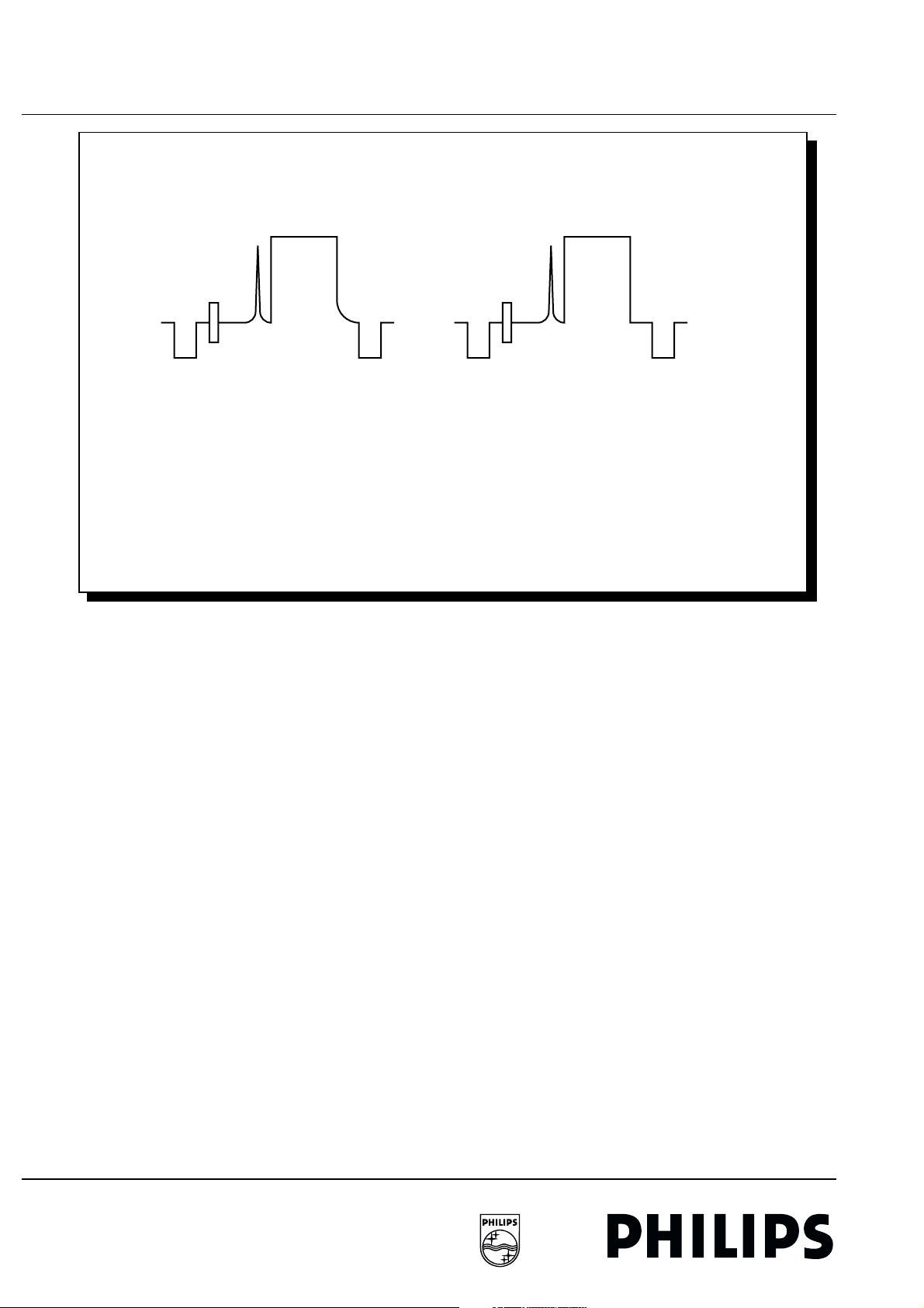
1 Offset = 4.5uA 1 Offset = 0uA
Phase alignment (R9G6)
• Connect a signal generator to (e.g. PM5326) to the tuner of
the set.
• Select a 475.25 MHz window signal (centre white) without
sound.
• Set the subchannel frequency 475.25 MHz in the DW mode.
• Connect an oscilloscope to TP20 and adjust R9G6 that the
shape of horizontal white black jump becomes as figure
above
CL 66532066_001.ai
Set TDA9143/44 in PAL plus mode ( HW option code nr 3 - bit
7 )
Measure Y-MAC on pin 2 of connector S62 or pin 2 of
connector S49 and align R3361 [S5] until the amplitude =
1.1Vblack-white5%
221096
M-trap alignment (L9G0)
• Connect a signal generator to (e.g. PM5326) to the tuner of
the set.
• Select a 475.25 MHz colour bar with 4.5MHz sound carrier.
• Set the subchannel frequency 475.25 MHz in the DW mode.
• Connect an oscilloscope to TP20 and adjust L9G0 to
minimum amplitude of 4.5 MHz sine wave on the sync-chip.
CVBS level adjustment on the Small Signal Panel
For this alignment it is necessary that the comb filter (module),
DW module and feature box are in the SSP.
For sets without PAL plus feature.
Input signal : Antenna test signal PAL 75% colourbar
Measure Y-FEAT on pin 1 of connector S48 and align R3361
[S5] until the amplitude = 1.0Vblack-white 5%.
For sets with PAL plus.
Input signal : Antenna test signal PAL 75% colourbar
Page 21
FTV1.9EE Receiver Box 4. Service modes 21
4.9 Software Alignments
4.9 Software Alignments
See chapter "Service Alignment Mode (SAM)".
Personal notes
Page 22
22 5. Audio FTV1.9EE Receiver Box
5.1 Audio Signal Flow
5. Audio5.1Audio Signal Flow
FRONT
END
S1
AUD1-TERR
AUD2-TERR
SIF-TERR
CINCH FRONT
CINCH VGA
CINCH DOLBY
CENTRE INPUT
DECODER
Scart 1
Scart 2
Scart 3
INPUT
FRONT I/O PANEL
INPUT
A/V BUFFER PANEL
SIGNAL FLOW
SCART
OUTPUT
7/26 13/20
MAIN IN
3/5
AUX IN
28/30
SCART IN
1/32
I-STEREO
PROCESSING
INCREDIBLE STEREO PANEL
HEADPHONE
OUTPUT
VOLUME
SPATIAL
TREBLE
BALANCE
CONTROL
10/239/24
AUDIO
CONTROL
BASS
ON/OFF
S3
LOUDSPEAKER
15/18
OUTPUT
FRONT I/O PANEL
S4
HEADPHONE
OUTPUT
CINCH CL/VL
OUTPUT
I/O PANEL
A/V BUFFER PANEL
CINCH VGA
OUTPUT
CL 96532069_040.eps
240899
PRC_IN
NC
NC
I/O PANEL
ECO NICAM PANEL
ECO NICAM
DECODER
G
L/R-TERR
L-2CS
S2
2CS
R-2CS
The selection Front_audio and the VGA_audio will first be done
at the A/V buffer. This output signal will go to the audio matrix
at the I/O board for the selection with the SCART inputs.
The Audio path can be divided in several building blocks:
• Front-end (S1)
• Terrestrial sound Decoding
• Source Selection
• Audio Processing (for loudspeakers headphones and CL)
• Loudspeaker Filtering and Power Amplifiers (for
loudspeakers and headphones).
The Loudspeaker filtering and Power Amplifiers are transferred
from the E-Box to the Monitor, so they are not described in this
document. The following part will describe the functions
realised in each building block in the E-Box.
Front-end (S1)
The front-end demodulates the sound information from the
terrestrial TV signal (VHF, UHF, S- and H-channels).
Two different tuners will be used in the FTV 1.9 project.
• The FQ916DME which is suitable for systems B/G, L and M.
(/12 - Western Europe)
• The FQ916DMF which is suitable for B/G, L/L' and I. (/19 -
France/UK)
FM demodulated audio signals (B/G, I and M) are available at
the AUD1_TERR and AUD2_TERR;
AM demodulated audio signals (L/L') are available at
AUD1_TERR.
NICAM can not be demodulated/decoded in the front end, and
must be realised by a separate NICAM demodulator/decoder.
Therefore the SIF_TERR signal is made available which
contains all sound subcarriers (amongst which the NICAM
subcarrier of 5.85 MHz or 6.552 MHz depending on the
system).
2CS decoder (S2)
The 2CS decoding is in fact de-matrixing of the two FMdemodulated carriers and pilot tone detection. The pilot tone
detection is needed to indicate if a transmission is mono, stereo
or bi-lingual. The status of the detection can be read out via I2C.
The software then knows how the de-matrixing must be set,
and must control that via I2C. For a bi-lingual transmission the
language can be selected via I2C in the stereo decoder.
The 2CS decoder IC has a source selector that selects between
the de-matrixed mono/stereo/ dual signal and the AMdemodulated mono signal (system L/L' for France).
NICAM sound decoder (G)
The NICAM demodulation consists of QPSK demodulation and
delivers a bit stream signal to the NICAM decoding. The NICAM
decoding interprets the bit stream and generates either mono,
dual language or stereo depending on the transmission. The
kind of transmission (mono, dual or stereo) can be read from
the SAA7283 via I2C. The software can select the desired
mode (E.g. language 1 or 2) via I2C.
Page 23
FTV1.9EE Receiver Box 5. Audio 23
5.1 Audio Signal Flow
The IC also has a register that contains the maximum allowed
Bit Error Rate (BER) of the digital sound reception. The main
SW has to write this max BER into this register. If the measured
BER becomes higher than max BER then the IC will switch
automatically to analogue sound to prevent crackling sound.
The SAA7283 contains a source selector that is used for
selection between analogue sound (FM mono/stereo or AM
mono) and digital (NICAM) sound.
The NICAM signal can be muted via I2C. During channel
switching also the TDA9840 is muted.
Euro I/O (I)
The Eco Euro I/O panel realises the source selection of the
SCART2 output, the loudspeaker and the headphone
channels. Only stereo pairs can be selected, so no language
selection can be done here. All switches can select between 5
stereo inputs, have a separate gain control, a separate mute
position, and a tri-state option. A switch can be set in a certain
position by writing a byte to the address of the TEA6430 on the
Eco Euro I/O panel.
Personal notes
Page 24
24 5. Audio FTV1.9EE Receiver Box
Dolby Receiver
VCR/DVD MONITOR
SCART
L/R AUDIO L/R CENTRE
E-BOX
SCART 1
SCART 2
SCART 3
CL/VL
OUT
DOLBY
RECEIVER
CENTRE
INPUT
CENTREL/R AUDIO
L-SURROUND
L-FRONT
R-FRONT
R-SURROUND
CL 96532069_006.eps
040899
Page 25
FTV1.9EE Receiver Box 5. Audio 25
5.1 Audio Signal Flow
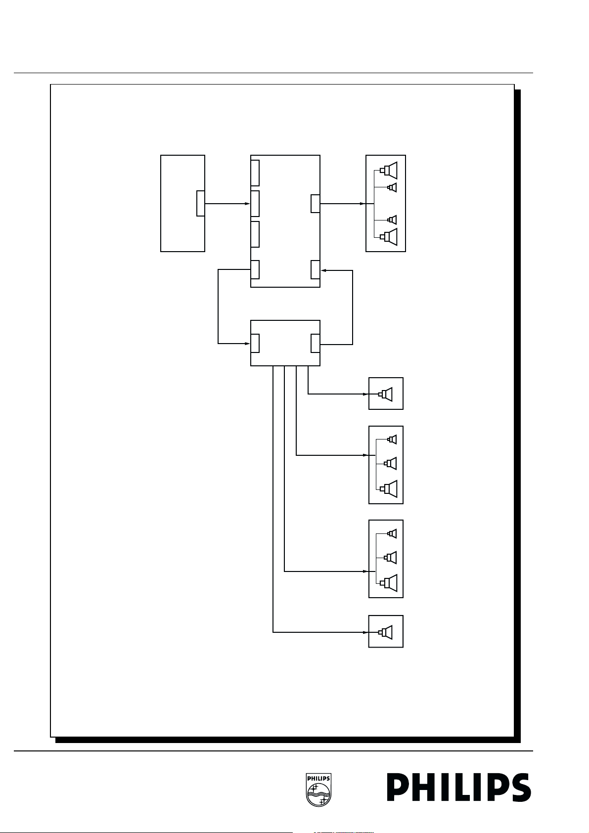
Connecting a Dolby Receiver:
The connection of the Dolby receiver
In the E-Box, no Dolby processing is done. However a Dolby
processor can be connected to the E-Box. Via a menu item, the
E-Box can be switched in a special Dolby mode, where the CL/
VL output will be a fixed value (CL out) of 0.5Vrms and the
Dolby input of the AV Buffer will be selected.
The External Dolby source must always be connected via
SCART or front Y/C or CVBS with L+R audio.
The Dolby audio signals will pass the source selectors for the
headphone and CL output.
At the AV buffer, the single Dolby centre signal will be split up
in the L and R audio signal for the Monitor (so the sound will be
audible via the left and right speaker).
The set speakers in the Monitor will be the centre speakers.
The headphone processing consists of volume, balance and
mute.
Personal notes
Page 26
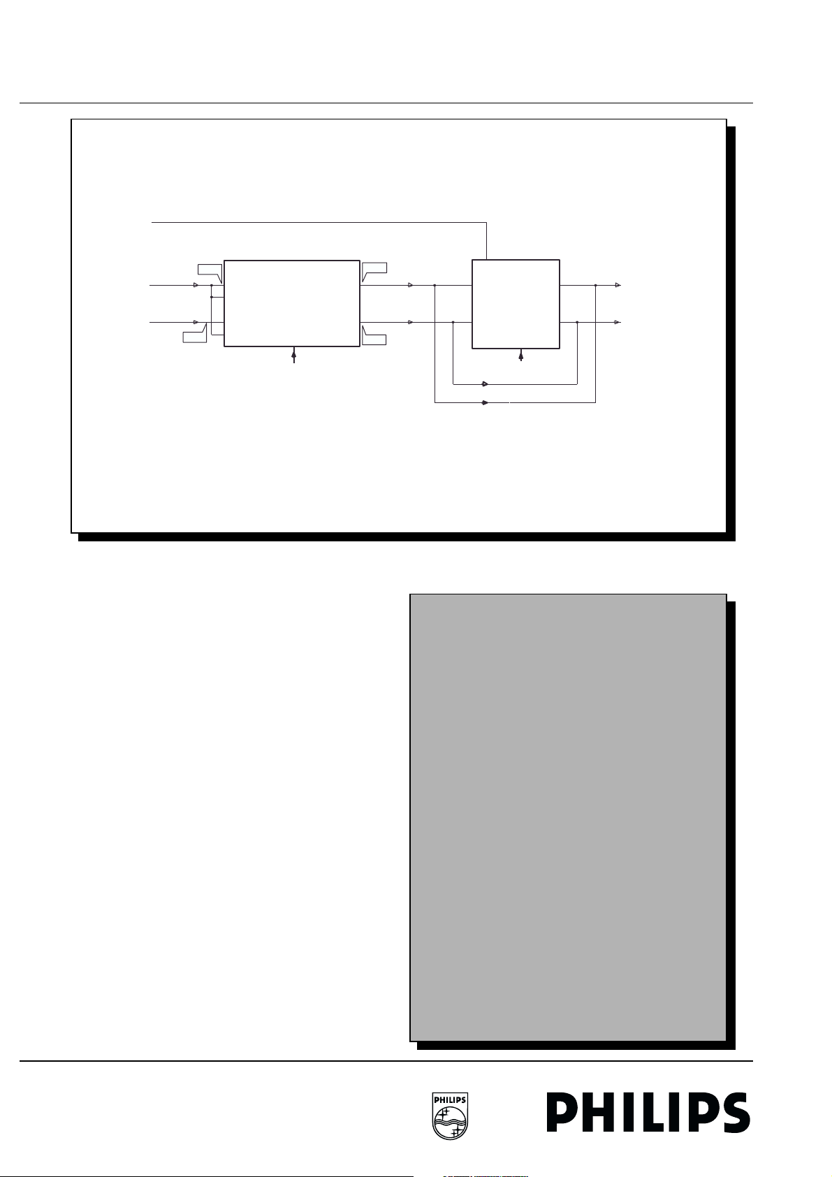
26 5. Audio FTV1.9EE Receiver Box
5.2 Audio processing
5.2 Audio processing
AUDIO PROCESSING
IF-NICAM
IC7600
TDA9840
Aud1-terr
M, I, L+R
Aud2-terr
II, 2R
S26
From Front-end
S26
7
9
2CS decoder
8
10
I2C
12
11
S27
M,I,II,L
M,I,II,R
S27
L-2CS
R-2CS
L-terr
R-terr
to
I/O
Panel
240899
Nicam
2
I
C
jumper if no NICAM
CL 96532069_029.eps
2CS SOUND PATH
The purpose of the 2 carrier sound decoders is to convert the
audio signals from the FM demodulators in the front-end into
mono, stereo or dual sound audio signals. In case a NICAM
module is present also the NICAM digital sound can be
selected. This selection takes place on the NICAM module.
The 2CS decoder is built up around the TDA9840 IC and
comprises:
• The stereo matrix.
• The de-emphasis.
• The output switch for mono, stereo, dual A/B and AM
sound.
• The output-mute.
• The mono, stereo, and dual identification.
Personal notes
Page 27
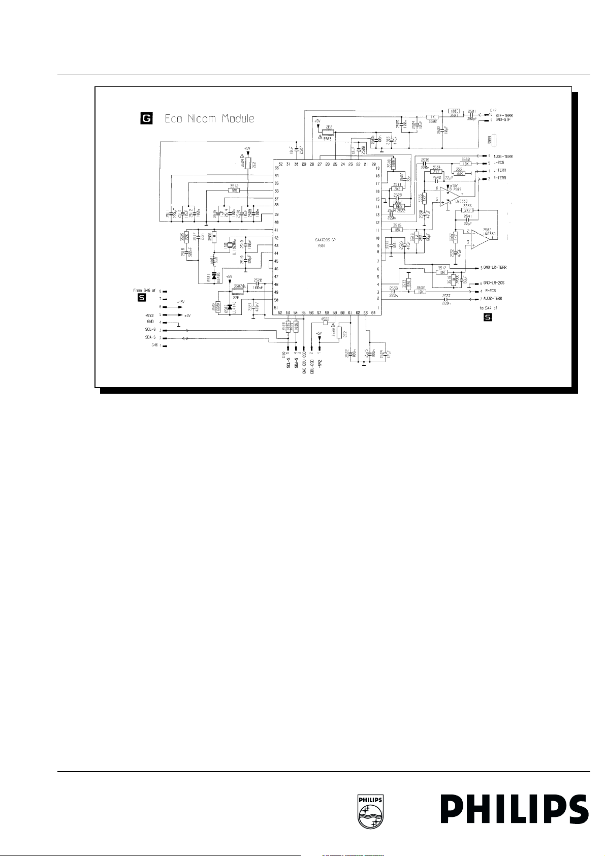
FTV1.9EE Receiver Box 5. Audio 27
5.2 Audio processing
The used IC is a SAA7283, which contains the NICAM
demodulation/decoding, and also the QPSK
demodulator so that the whole circuit is build around the
IC7501.
The IC7501 contents:
• FM and vision filters, analogue demodulator and switching
• Dual standard with automatically system selection
• Stereo Bitstream audio DAC´s
• Programmable attenuator for matching levels of NICAM
and FM audio sources
•µP controlled via I2C -bus
NICAM sound path
Signal-processing:
• The SIF-signal originating from the front-end is sent to the
pins 28 and 29 of the SAA7283
• After amplification the signal is offered to the internal QPSK
demodulator; the signal will then demodulated and
converted back to a bit stream of 728K.
• The NICAM decoder-part of the IC decodes the signal. A
digital filter provides error correction and increases the
sample frequency by a factor of three. The two DAC's
integrated into the SAA7282 convert the signal into an
analogue signal. Finally, a switch in the SAA7282 selects
between NICAM signals or analogue signals.
• The kind of NICAM-transmission (mono, dual, stereo) and
also the allowed Bit Error Rate (BER) can be read out via
I2C -bus; by using this information a decision whether
CL 96532069_041.eps
130799
NICAM or analogue sound is audible can be determined by
the µP.
• The signal from the 2CS-decoder IC7600 (TDA9840) is fed
to the pins 3 and 12 of the SAA7283.
• The selected output signal (pin 4 and pin 11) is delivered to
an amplifier-stage, build up with a LM833.
• Finally the signal is then offered to the source select I/Opanel.
Page 28
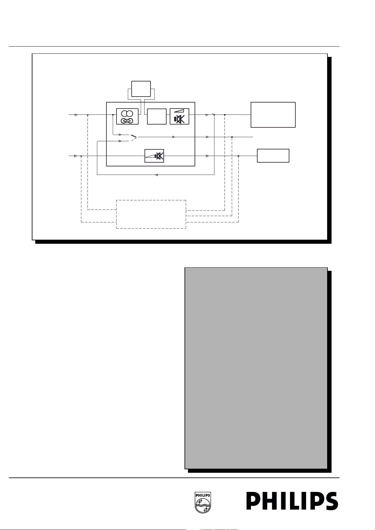
28 5. Audio FTV1.9EE Receiver Box
5.3 Audio Control
5.3 Audio Control
AUDIO CONTROL
Incr.
Sound
IC7650
TDA 9860
From
I/O select
main
hp-ss
3
5
1
32
28
30
cst.
var.
audio control
audio feature unit
tone
cst./var.level
o
o
o
headph.
General
All necessary adjustments such as volume, tone, stereo, mono,
spatial, mute, etc. are performed in the control IC TDA9860. An
internal switch can pass the sound through the incredible sound
panel. This signal is sent to the audio output amplifiers.
The "headphones" sound that has a separate selection switch
on the I/O panel travels via volume and balance controls to the
headphone amplifier.
The audio output on the I/O panel can be switched between a
constant and variable level.
All switching and adjustment are performed via I2C-Bus.
18
7
26
13
20
Personal notes
prc15
cl/vl
audio power
ampl.
I/O panel
o
var./const
level out
head.amp.
hp-out
CL 96532069_030.eps
240899
Page 29
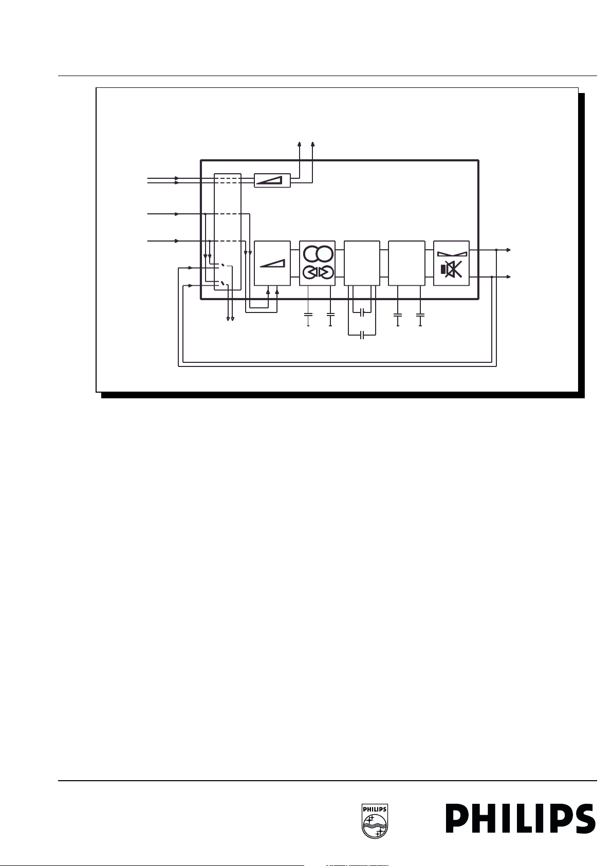
FTV1.9EE Receiver Box 5. Audio 29
5.3 Audio Control
AUDIO CONTROL IC
headph.ampl
R-HP-out
1320
soundprocessing
bass
12
27 29 22
2652
2654
11
15n15n
2656
33n
2658
IC 7650
To
audio
ampl.
R-PRC
15
treble
14 19
21
2660
5.6n
5.6n
2662
L-PRC
18
From
I/O panel
L-HP-SS
R-HP-SS
L-MAIN
R-MAIN
28
30
3
5
32
TDA 9860
input
select
o
o
o
1
o
L
const./var.level output
I/O panel
L-HP-out
o
o
726
R
2491023
L
R
Block diagram control IC - TDA9860
The audio control IC7650 (TDA9860) on the SSP has 3 stereo
or 6 mono inputs and 6 outputs. Each input can be switched to
an output.
The loudspeaker channel
The audio from the I/O-panel is fed to the input pin 3 and pin 5.
Following volume adjustment the selection for stereo, spatial
with two positions and mono with or without pseudo stereo
effect is made. The tone adjustment consists of a bass
adjustment (C2656 and C2658) and a treble adjustment
(C2660 and C2662).
The loudness adjustment is a volume dependent tone
adjustment that operates on signals smaller than 10 dB.
Balance adjustment follows the tone adjustment. On mute the
volume is switched to minimum. The output pin 18 and pin 15
respectively carry the left and right audio signals that are sent
to the amplifier.
The constant/variable level output
A connecting plug is located on the I/O panel with which the set
can be connected to an audio installation. This plug is
connected to the outputs pin 7 and pin 26 that can be switched
to the constant level signal from pin 3 and pin 5, or the adjusted
signal for the output amplifier that is fed back to the inputs pin
1 and pin 32.
CL 96532069_031.eps
240899
Headphone output
The headphone adjustments are performed on the I/O panel.
The audio signal incoming from the I/O-panel is delivered to pin
28 and pin 30 on the control IC. Following volume and balance
adjustment the signal travels to the headphone amplifier via
outputs pin 20 and pin 13.
Page 30
30 5. Audio FTV1.9EE Receiver Box
5.4 Incredible Stereo (AY-panel)
5.4 Incredible Stereo (AY-panel)
INCREDIBLE STEREO (AY-panel)
PHASE
SHIFT
L
+
+
L
R
PHASE
SHIFT
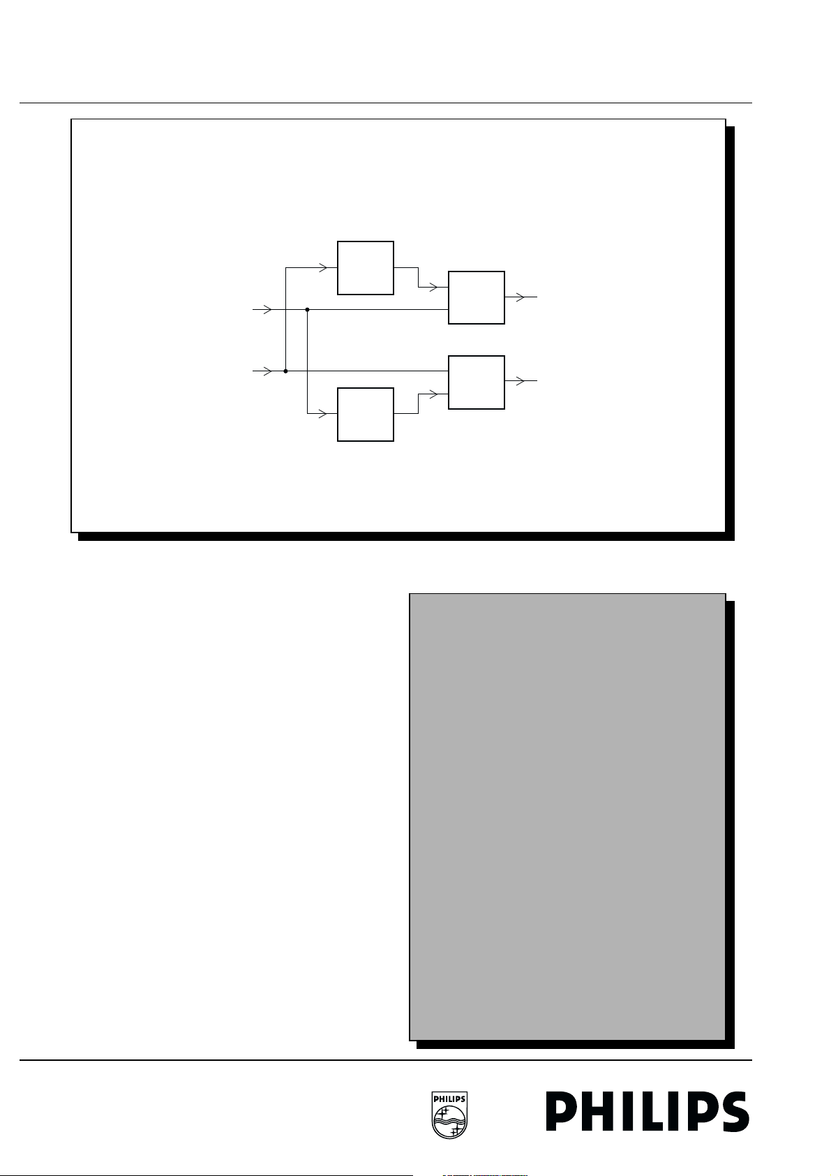
The principle of the incredible sound processing is based on the
fact that the human mind mainly uses two elements for
localising a sound source. When a sound comes from the left,
it will enter both ears but:
• The phase of the sound will be slightly different for both ears
because of the distance between the ears.
• The sound level will also be slightly different, also because
of the distance between the ears.
The incredible sound circuit electronically generates a phase
and sound level relation between the left and right signal, in
such a way that to the human mind it sound as if the sound is
actually coming from the far left or right side.
The circuit itself therefore consists of two phase shift circuits
and two adder circuits. In this way a bit of the right signal is
added to the left signal and visa versa. The adding is done with
a carefully selected phase shift and amplitude relation.
The source-audio-signal incoming from the IC7650 (TDA9860)
Pin 9 and 24 is delivered to the incredible
surround panel.
For the incredible sound function two LM833T (IC7600/IC7601)
are used; one part of the IC´s are used for the phase shifting,
the second part is used for amplification.
The signal is then fed to IC7602, which works as a switching-IC
between the original audio-signal and the "incredible sound"signal.
The selected signal is then routed back to the TDA9860 pin 10
and 23 for further processing.
+
+
CL 96532069_007.eps
040899
Personal notes
R
Page 31
FTV1.9EE Receiver Box 6. Video 31
6.1 Introduction
6. Video6.1Introduction
For the block diagram see Service Manual Receiver Box
chapter 6.
• The FRONT-END transmits a video signal to the InputOutput panel. The LF audio signals originating from the 5.5
and 5.7 MHz carriers are processed into stereo or dual
signals in the 2CS (2 Carrier Sound decoder).
• The Nicam signal is transmitted to the Nicam decoder as an
IF signal. The Nicam decoder processes the signal into
stereo or dual signals and also provides the switching
between Nicam and non-Nicam signals. The switched LF
signals are sent to the Input-Output panel.
• The INPUT-OUTPUT PANEL accommodates 3 scart plugs
and an audio output with cinch plugs. The front signal and
the SVHS input are transmitted to the Input-Output panel.
The signal selection is located on the panel itself and
includes the audio switch, the video switch that switches
CVBS or SVHS, the RGB switch and finally the record
selection that transmits the signal selected to SCART 2.
The panel has its own microprocessor that communicates
with the main processor via IC.
• In sets without Dolby Pro Logic the audio controls are
performed on the SSP panel. The outputs of the audio
controller supplies the headphones amplifier, the audio
output and the L and R output amplifier.
• The selected source for the video signal is transmitted to the
COMB FILTER that offers separate Y and Chroma to the
chroma decoder. The comb filter is deactivated for SVHS
and SECAM signals. The chroma demodulator processes
the signal into U and V signals, and transmits them together
with the Y signal to the Feature Box. The chroma
demodulator also accommodates the sync. section, the
sync. pulses are also transmitted to the Feature Box.
• The Double-Window module contains a second tuner and is
in that case supplied with antenna signals. The DW module
can also work with CVBS or SVHS signals. In the Double
Window module a sub-picture can be inserted via a fast
video-switch IC. The output of the DW module is fed to the
feature box.
• The Feature Box receives 50 Hz signals and converts them
into 100 Hz signals. In the feature box digital scan,natural
motion and AI is applied. Other features can be switched on
as required.
• The 100 Hz signals are matrixed into RGB signals in the
video controller (TDA4780). Video adjustments are then
performed via IC. TXT or OSD signals are selected by the
video control IC.
• The audio amplifier and the supply for the Monitor have
been moved from the E-Box to the Monitor while the Dolby
processing has been deleted. The small signal electronics
is "taken over from/based on" the GFL-Feature Lift (GFLFL) because this is a very versatile (global) High End
chassis .
Personal notes
Page 32
32 6. Video FTV1.9EE Receiver Box
6.2 Tuner / Front-end
6.2 Tuner / Front-end
FRONT - ENDS
FQ916ME Mk2
23
22
25
AF1/AM
27
AF2
240899
CVBS
Nicam
5.85
A
HF
11
33V
FQ916MF Mk2
FQ916DME Mk2
FQ916DMF Mk2
FQ916MR Mk2
HF IF
mixer
HF
Vtun.
PPL
ref.
osc.
2
I
C
13 14
osc.
f
o
band
34.4Mc saw BG
M
M
L
afc
I2C
BG/L
4.5/5.5/5.74/6.5
video
demod.
PLL
77.8
afc
sound
demod.
L
LM
M
IF
oo
o
AM
32.4
o
FM
4.5
FM
5.5
FM
5.74
TDA9815
ooo
CL 96532069_010.eps
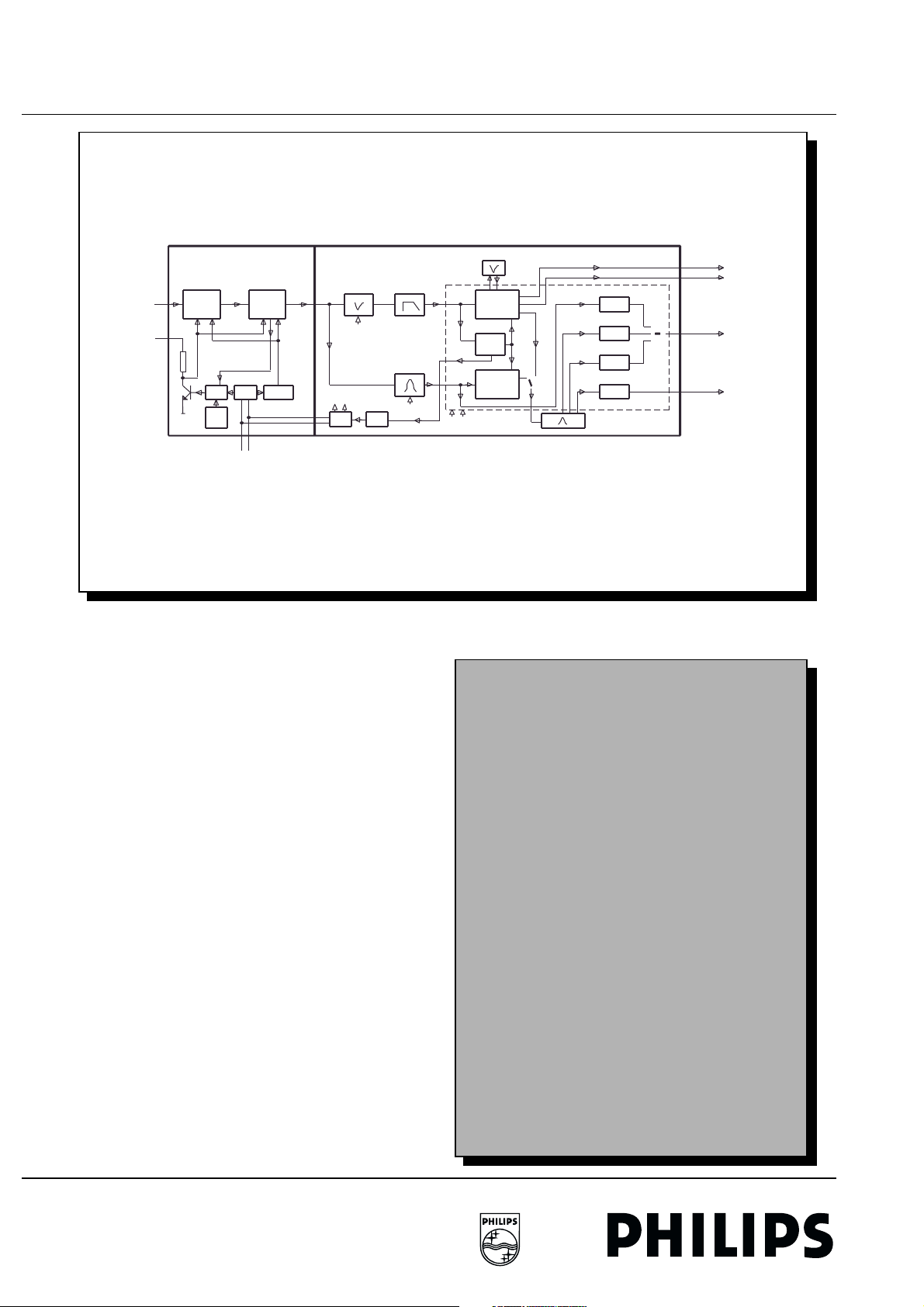
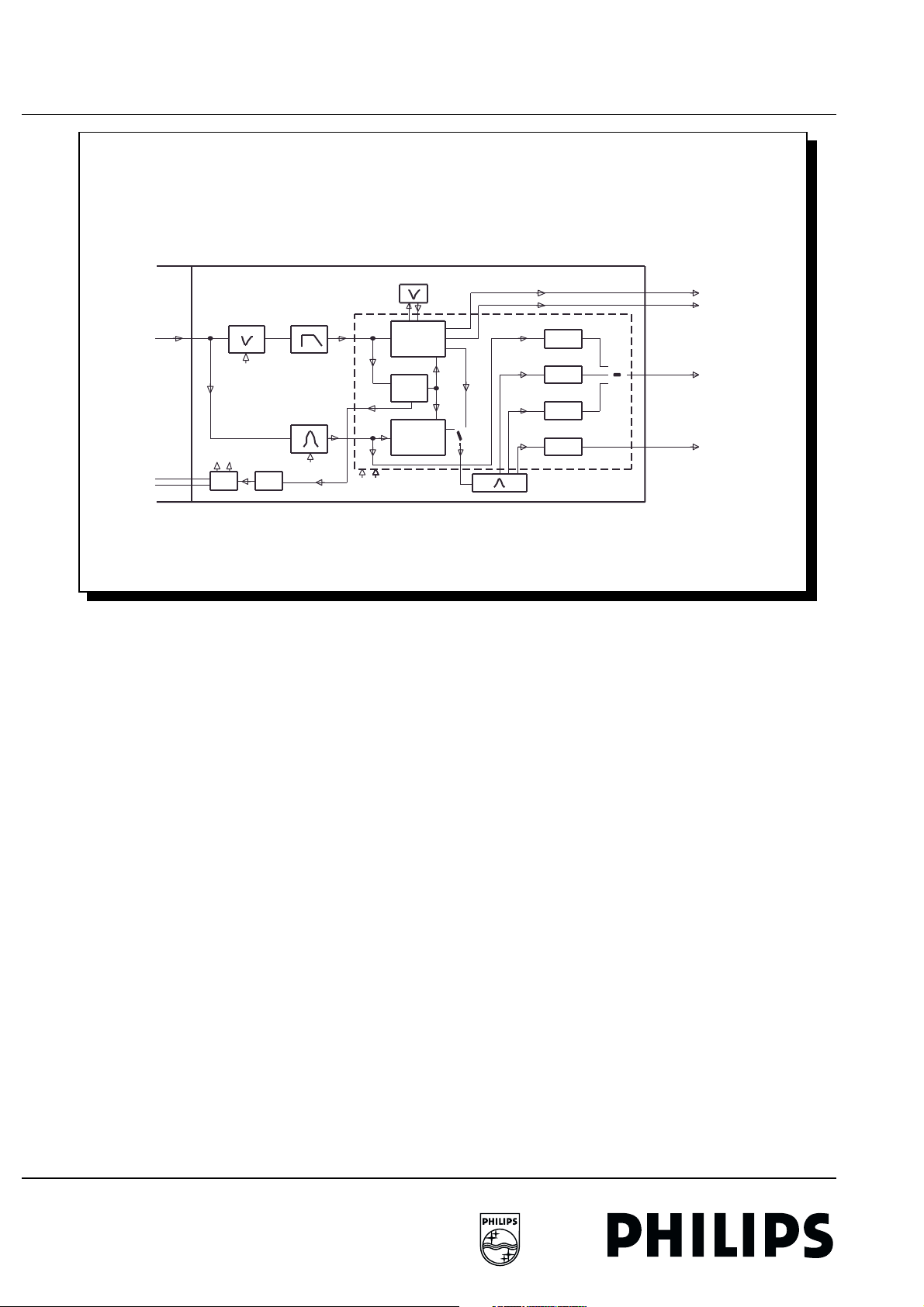
The front-ends used consist of:
• A tuner
• An IF circuit
• A detection circuit.
The tuner is suitable for the reception of VHF1, VHF3, UHF, Schannels and hyperband. The output supplies the CVBS
picture and a mono or stereo audio signal. The following types
are used within the FTV 1.9:
• FQ 916 DME/PH MK2 BG/L/M.
• FQ 916 DMF/PH MK2 BG/L/L'/I.
The following abbreviations are used in the names:
PH = PHono antenna connection.
D = Version with splitter.
MK2 = improved model in the 900 series with a wider bandpass
range in the tuner and better stabilisation.
Personal notes
Page 33
FTV1.9EE Receiver Box 6. Video 33
6.2 Tuner / Front-end
TUNER PART
FQ916
HF IF
A
HF
mixer
osc.
HF
11
33V
Vtun.
PPL
ref.
osc.
13 14
FRONT-END
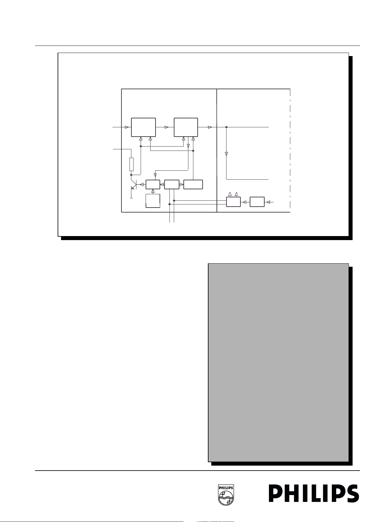
The tuner section contains the tuning stage and a combined
oscillator-mixer. The tuner is IC controlled. The full tuning range
is divided into a low, mid and high band.
Tuning is achieved by sending a frequency (divider) to the PLL
in the tuner. This adjusts the varicap voltage of the local
oscillator until the correct frequency is reached. By comparing
the frequency of the local oscillator in the PLL with the
frequency of a reference oscillator the frequency set via IC will
always remain constant.
When tuning the operation control software adjusts the
frequency to the correct AFC adjustment via the IC bus. The
frequency is stored in memory.
For VCR presets the AFC information is read out continuously
and the tuning adjusted if necessary.
The tuning voltage varies with the frequency selected.
f
o
2
C
I
band
Video
Audio
M
L
I2C
afc
CL 96532069_011.eps
Personal notes
240899
Page 34
34 6. Video FTV1.9EE Receiver Box
6.2 Tuner / Front-end
IF-PART
FQ916
IF
34.4Mc saw BG
M
M
L
afc
I2C
BG/L
L
4.5/5.5/5.74/6.5
afc
LM
IF and Detection
THE EUROPEAN MULTI, BG / L / M
In the 34.4 MHz filter the sound carrier for the M-norm is
suppressed so that it falls within the video bandwidth. Picture
detection is performed in the TDA9815 after the 38.9 MHz SAW
filter. In this case the reference frequency is not derived from
the picture carrier, but from a PLL oscillator on the double
frequency (this is 77.8 MHz). This is "locked" to the picture
carrier. The demodulator output supplies CVBS. For the L-norm
the positive video is inverted. External filters suppress the
sound carriers in each norm.
The sound carriers are filtered out of the IF. Following
synchronisation demodulation the FM sound carriers are set at
5.5 and 5.74 MHz.
The 4.5 MHz is derived from the video detection. A filter splits
the different sound carriers from one another. Following FM or
AM detection the AF1/AM output supplies the LF sound L + R,
language I or mono. Output AF2 supplies the 2xR LF sound or
the 2nd language. On mono or AM sound output AF2 is
suppressed automatically.
On incorrect tuning the PLL will be readjusted to the wrong
picture frequency. The PLL tuning is communicated via the I2C
bus as an AFC voltage. The tuning can then be readjusted by
the software.
video
demod.
PLL
77.8
IF
sound
demod.
CVBS
o
ooo
23
22
25
27
240899
AM
32.4
FM
M
oo
o
4.5
FM
5.5
FM
5.74
TDA9815
CL 96532069_012.eps
Nicam
5.85
AF1/AM
AF2
THE FRENCH MULTI BG / L / L' / I
Operation is the same as the European multi for the BG and Lnorm. The L'-norm provides several changes. A 40.4 MHz filter
suppresses the sound carrier of L'.
The SAW filter has an extra flank on 33.95 MHz, the sound
carrier on L'. The VCO of the PLL can be switched to 67.9 MHz,
the double frequency of the sound carrier on L'. The various
filters are also different in comparison to the European multi.
Page 35
FTV1.9EE Receiver Box 6. Video 35
6.3 I/O panel
6.3 I/O panel
I/O MICROPROCESSOR
+5
INTERRUPT
IC7814
EXT 1
STATUS
EXT 2
STATUS
4
9
7817
7817
B
LEVEL
B
LLVLL
TMP J7C2C3
15
6
5
4
28 22
16:9 STATUS EXT 1
4:3
16:9
4:3
11
9
8
17
RGB EXT 2
RGB EXT 1/EXT2 Kill
RGB EXT 3 Kill
EXT 3
STATUS
FBL Ext 1
RONI
OSDECT
RATIA
5
7816
B
LLVLL
26
16:9
25
4:3
24
27
PCR SDA SCL
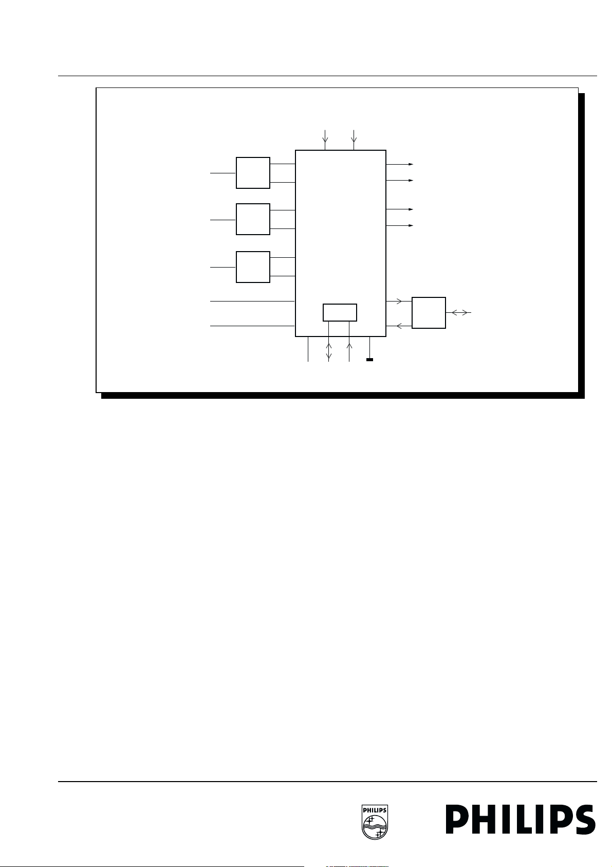
For this purpose the ECO-I/O-Panel from the GFL-chassis is
used.
It contains three scart-connectors and one front-input wich can
handle CVBS orY/C-signals.
A separate I/O- microprocessor, located on the I/O-PCB,
controls the input and output signals.
A cinch output delivers a audio-signal with variable or fixed
output.
Microprocessor
An extra microprocessor is present on the Input-Output panel
that steers all the control signals on the panel. The
microprocessor is supplied with a 5V power supply (stand-by
power supply) and receives a reset pulse from the POR which
is inverted by TS7800. The other pins are input or output pins.
The status signals for the three scarts have 3 levels: no status,
16/9 status and 4/3 status. For this reason they are first
converted into 6 signals in a comparator circuit (1 or 0).
Outputs are the RGB selection signal for scart 2 and RGB kill
for scarts 1 and 2 combined and for scart 3. Also the status
output pin for scart 1 is an output. Communication with the main
processor is performed via IC, a control signal IRQ-SS
(Interrupt ReQuest Source Select) warns the microprocessor if
any change has occurred. The main processor controls the
various switching IC's via IC.
The IRQ-SS provides status changes to the control processor.
When one of the statuses becomes active it is processed by
IC7814, which reports it to the central processor via the
7
2
C
I
3131214
16
interrupt line. The central processor halts its program and
requests the information via the IC bus. Depending on the
nature of the information the central processor will then signal
the switching IC's or the local processor IC7814.
The local processor does communicate via the IC bus but
therefore a 3rd line (strobe) to the main processor is required.
This uses the same pin as the interrupt, namely pin 22.
Reset
When the reset pin (pin 3) is held low while the power supply
voltage is present the microprocessor program will restart.
Furthermore the I/O microprocessor performs a self-test, the
result of which is made available via pin 21. If this is low the selftest was successful.
I/D
CL 96532069_037.eps
011099
Page 36
36 6. Video FTV1.9EE Receiver Box
6.3 I/O panel
EURO I/O VIDEO PATH
Video path Eco-I/O
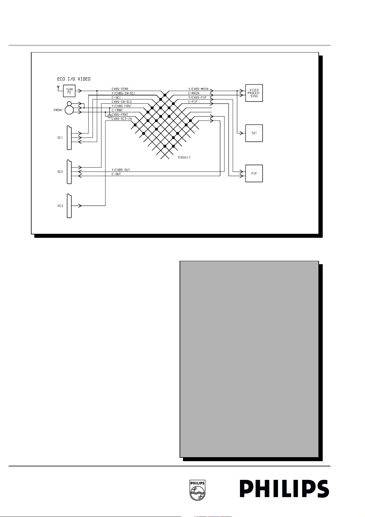
Input signals:
• +++++++++++++++++CVBS Tuner
• CVBS/RGB Euroconnector 1
• CVBS/Y-C/RGB Euroconnector 2
• CVBS Euroconnector 3
• Y/CVBS Front input
• C Front input
Output signals:
• EXT 1 --> CVBS terrestrial output
• EXT 2 --> CVBS or Y/C output C main picture / WYSIWYR
• EXT 3 --> only input
CL 96532069_013.eps
Personal notes
240899
Page 37
FTV1.9EE Receiver Box 6. Video 37
6.3 I/O panel
EURO I/O AUDIO PATH
+8V6 +8V-AUD
6851
1LL4148
4E7
IN
OUT
3800
2800
47uF
L-IN-SC1
L-IN-SC2
L-FRNT
L-IN-SC3
L-TERR
L-MAIN
R-MAIN
L-OUT-SC1
R-OUT-SC1
2887
220n
2806
10uF
REF
2804
10uF
2805
10uF
47uF
2802
10uF
2810
10uF
1
2817
223
4
5
6
7
8
9
10
11
12
TEA6430
GND
REF
VCC
L1-I
L2-I
L3-I
L4-I
L5-I
LI-O
R1-O
L2-O
R2-O
7822
SDA
SCL
SUB
R1-I
R2-I
R3-I
R4-I
R5-I
R4-O
L4-O
R3-O
L3-O
24
223
21
20
19
18
17
16
15
14
13
3872
100
100
3871
2813
10uF
2808
10uF
2812
10uF
2814
10uF
2811
10uF
SDA-S
SCL-S
R-IN-SC1
R-IN-SC2
R-FRNT
R-IN-SC3
R-TERR
R-HP-SS
L-HP-SS
CL 96532069_014.eps
OUT
040899
IN
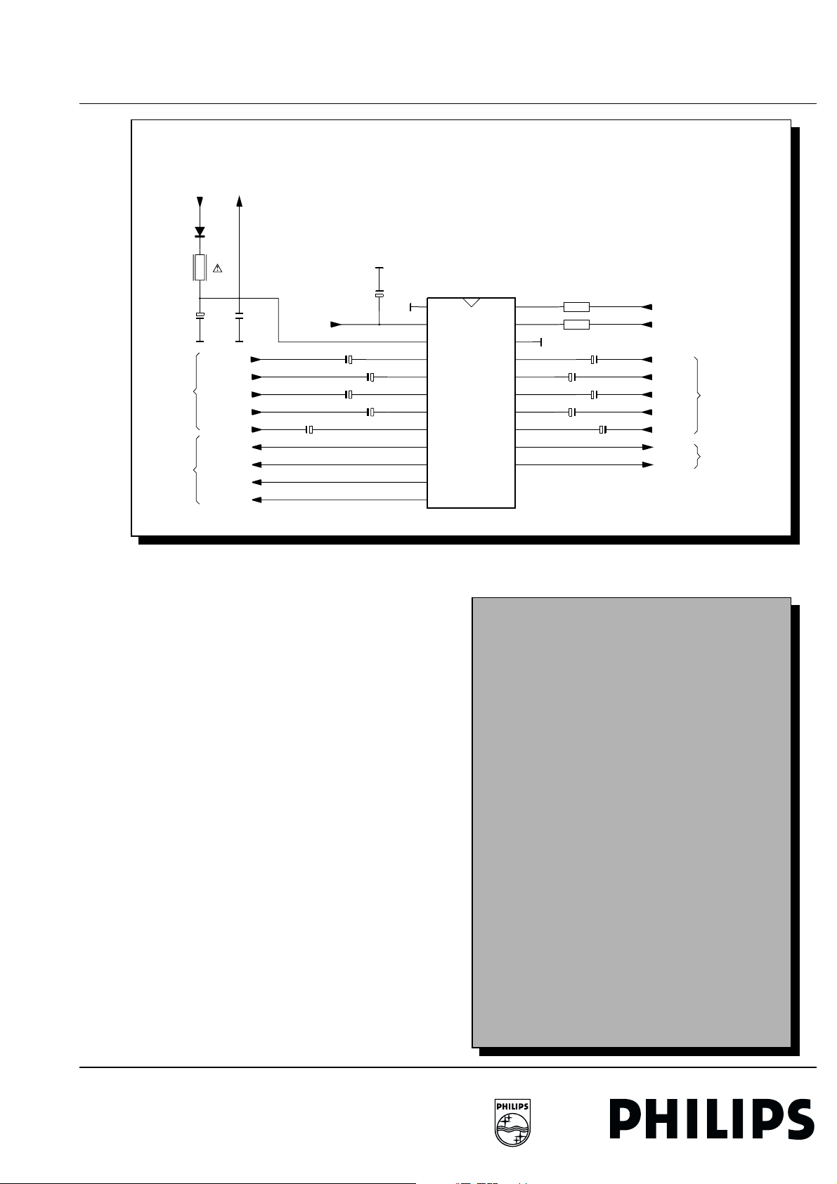
Audio path Eco-I/O
One switching IC is applied on the ECO I/O
Input signals:
• L/R Front-end
• L/R Front input
• L/R Euroconnector 1
• L/R Euroconnector 2
• L/R Euroconnector 3
Output signals:
• L/R Loudspeakers
• L/R Headphones
• L/R Euroconnector 2 out
DUAL
An extra feature of the EURO-I/O panel is that a choice can be
made between language I and II for both loudspeakers and
headphones because the front-end sound is supplied to 2
inputs.
Personal notes
Page 38
38 6. Video FTV1.9EE Receiver Box
6.3 I/O panel
EURO I/O RGB PATH
RGB path Eco-I/O
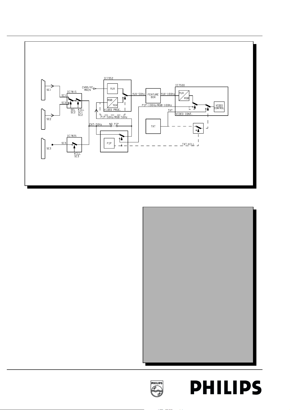
In sets with an ECO-I/O there is only one RGB input which is
selected by IC7815 whether RGB originates from SC1 or SC2.
This RGB signal is fed directly to the TDA9144 bacause no PIPmodule is present; the chroma-IC converts the RGB into YUVsignals. This YUV signal is carried via the feature box to the
video controller.
Personal notes
CL 96532069_035.eps
240899
Page 39
FTV1.9EE Receiver Box 6. Video 39
6.4 Video-signal processing
6.4 Video-signal processing
BLOCK DIAGRAM VIDEO
Video Processor
Decoder + Sync
Video
Dem.
YUV
RGB
Sync
Va
Ha
SC-1FH
RGBscart
RGBscart
Main
Y/CVBS
C/CVBS
Comb.filter Feature Box Video Control
Combf.
PAL
NTSC
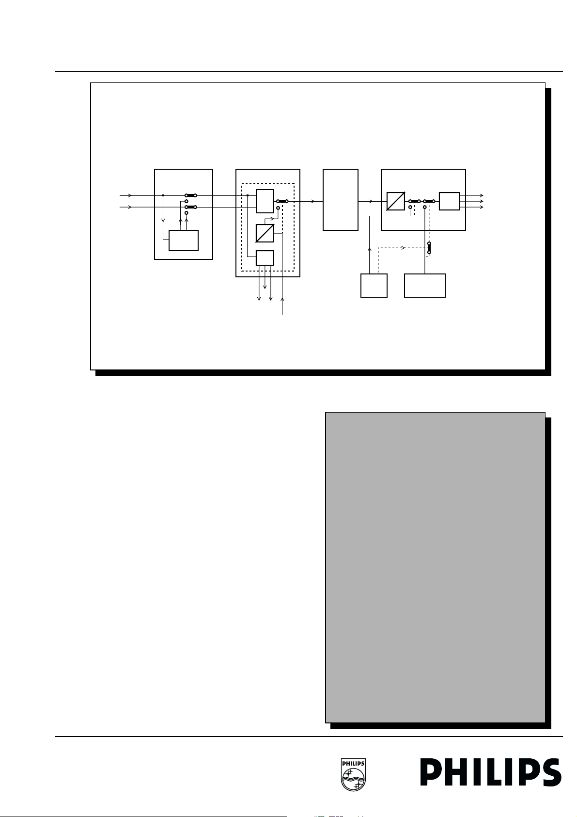
Just before the video processing, the CVBS is adjusted to stop
the amplitude spread in the circuits before the video
processing. This is necessary for the optimum performance of
the circuits that follow.
In the video processing the CVBS originating from the I/O panel
in PAL and NTSC are switched through to the comb filter where
Y and chroma are separated. In SECAM the required chroma
and luminance filters are located in the chrominance decoder.
An SVHS signal with separate Y and chroma is switched
directly to the decoder. In the decoder Y and chroma are
converted to Y, U and V. The synchronisation provides a 50 Hz
horizontal, vertical and sandcastle pulse.
Y, U and V are doubled within the FBX-4 to a line frequency of
32kHz. The frame frequency remains 50Hz. The PDP can can
not handle frequency above 72Hz.
In the video control circuits Y, U and V are converted to RGB.
With a switch, TXT or OSD can be switched on.
The switched RGB signals undergo the following adjustments:
brightness, contrast, saturation and black-stretch.
The 100 Hz picture is carried to the video control.
YUV
50Hz
50Hz
AI print
PALplus
PIP
50Hz
50Hz
YUV
YUV
RGB
TXT-kill
PIP TXT-OSD
Personal notes
Control
CL 96532069_015.eps
011099
PTP
R
G
B
Page 40
40 6. Video FTV1.9EE Receiver Box
6.5 Comb filter circuit
6.5 Comb filter circuit
COMB FILTER
K
7352
23
FSUB/COMB ON-OFF
VIDEO PROCESSOR
TDA 9141
26
Y/CVBS-COMB
25
C/CVBS-COMB
V10a
(Y/CVBS_COMB)
0.2V / div AC
10µs / div
V10b (C/CVBS_COMB)
0.2V / div DC
10µs / div
(FSUB_COMB
ON/OFF)
V12
0.1V / div AC
0.5µs / div
CL 96532069_038.eps
240899
Y/CVBSMAIN
C/CVBSMAIN
Q
3422
2406
2407
17
Y
10
C
13
FSCSW
16
TMSEL
4
TP2
+5
786
VCC
VCCO
/CVBS
EXT
EXT
DGND
OGND
21 11 9 26
4234
4233
2423
2405
2404
2403
19 24 5 25 3 1
CSY
SSYN
AGND
REFDL
REFBP
COMB FILTER
SAA4961
PLLGND
SYS2
SYS1
23 20 18 27 22
COMBENA
LPFION
3421 4.43MHz
BYP
FSC
Y
OUT
C
OUT
VCCPLL
VDD
5402
2417 2402
5401
2416
2401
V12
V10a
14
12
V10b
+5
+5
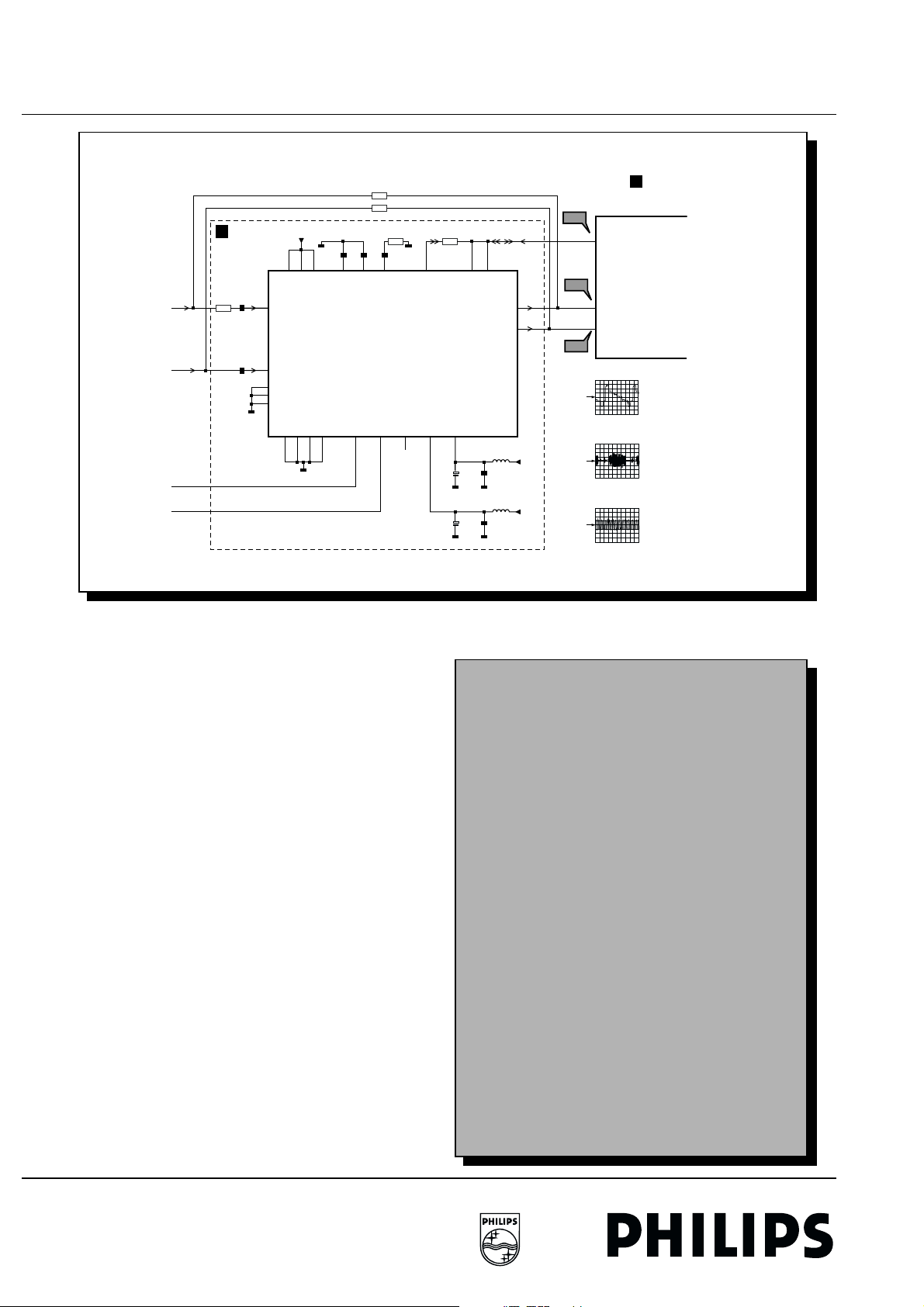
The comb filter IC is located between the I/O-panel and the
video-processing IC TDA9144.
It can work in two different conditions:
• Comb filter mode
• By-pass mode
The voltages at pin 20 and 23 of the SAA4961 (SYS1 and
SYS2) determine the current mode
PAL + NTSC-input signal: --> comb filter "on" --> Pin 14 delivers
the Y-out signal --> Pin 12 delivers the C-out signal
SECAM + SVHS-input signal: --> comb filter "off"
The system pins are connected to the I/O-controller HEF 4094
(IC7204) which is controlled by the µP.
Personal notes
Page 41
FTV1.9EE Receiver Box 6. Video 41
6.6 Video processor (IC7352)
6.6 Video processor (IC7352)
VIDEOPROCESSING
chr.
y/cvbs
clock
combf.
7352
chroma
25
switch
del.
26
60n
23
sync
sch.
hor.
PLL
3354
24k
2368
470n
c
o
o
o
y
y
filt.
vert.
sync
24
sc-1Fh
2370
2n7
Pal-NTSC
timing
gen.
17
clamp
sec.
cl.
filt.
DC
o
o
o
o
o
o
o
o
o
in
Secam
Dem.
Pal
NTSC
Dem.
hue
chr.
PLL
30 31
4.43 3.58
15p 15p
sys.id.
+
17
11
Ha
Va
syst.
switch
29
3376
2392
100n
y
YUV
75k
TDA9144
-(r-y)
-(b-y)
outp.
switch
RGB
clamping
TDA46657358
2393
16
100n
2394
1
14
2
100n
sc-1Fh
U
3
V
4
13
14
12
18
21
20
19
2391
2n2
5
V
U
Y
F-Bl.
R
G
B
-dec
-dec
-dec
64u
64u
PLL
to FBX
from PIP
+
+
CL 96532069_016.eps
11
12
100n
2396
100n
2395
UV
240899
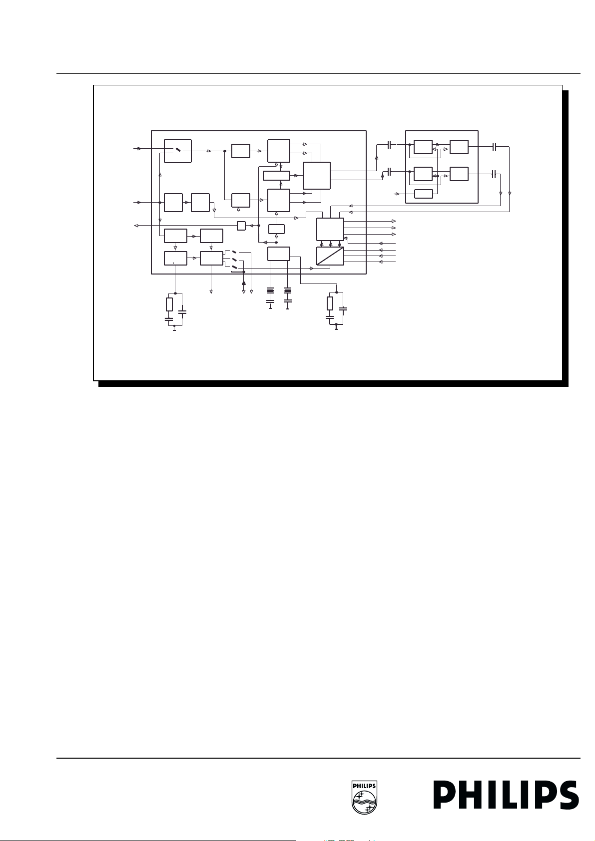
The TDA9144 is an IC controlled PAL-SECAM-NTSC decoder
with a built-in sync processor. The number of peripheral
components is very limited and there are no adjustments.
The luminance path
The luminance signal from pin 26 is delivered via the delay line
to the Y filter. This filter is switched automatically depending on
the colour system. When the comb filter or the external SECAM
notch filter is switched on the filter in the IC is switched off. The
Y signal travels directly to the output switch.
The chroma switch
The chroma switch connects the CVBS or the chrominance
signal to the demodulator. This switch is placed in the required
position by IC. In the automatic mode the signal with the largest
burst is switched through. A picture originating from the frontend comb filter therefore provides a separated chroma. On
poor reception the comb filter does not work and the CVBS is
used.
The colour demodulator
After the chroma switch the signal, depending on the colour
system, travels either to the chroma bypass or the SECAM
clock filter. When the comb filter is operative, the filters in the IC
are switched off. The PAL/SECAM or NTSC demodulator
provides the -(R-Y) and -(B-Y) signals that are switched via the
system switch to outputs pin 1 and pin 2.
The chroma delay IC ( IC7358)
The operation of the delay IC is the same for the different colour
systems; the purpose however is dependent on the system. In
the PAL system phase errors are removed. On SECAM,
whereby both the -(R-Y) and the -(B-Y) output of the
demodulator only contain colour every other line, the missing
line is filled in by the previous delayed line.
RGB matrix and output switch
The U and V signals from the delay line are delivered together
with the internal Y signal to the output switch. A selection can
be made here between the signals originating from the
demodulator and RGB from the I/O-panel. The switch is
normally positioned via IC. Switching can also be made
dependent on the voltage on pin 18 of the IC, control then
occurs through the RGB fast blanking. The RGB signals are
converted in the matrix into Y, U and V and are present at pin
12, 13 and 14 of IC7352.
Identification and PLL
The crystals used determine the recognisable colour systems.
The 4.43 MHz ( pin 30 ) and 3.579 MHz crystals ( pin 31 ) used
make the decoder suitable for PAL and NTSC on both
Page 42
42 6. Video FTV1.9EE Receiver Box
6.6 Video processor (IC7352)
frequencies. For NTSC the reference oscillator phase is
regulated in the HUE adjustment.
The 4.43 or 3.579 MHz reference frequency that is used as the
clock frequency for the comb filter is located on pin 23. This is
superimposed on a DC voltage that switches on the comb filter.
The DC voltage can be switched on or off via IC, which in turn
switches the comb filter on or off.
Personal notes
Page 43
FTV1.9EE Receiver Box 6. Video 43
6.7 Video control
6.7 Video control
LUMINANCE TRANSIENT PROCESSING
sandcastle
Y
1
3
2
5
U
9
Delay
V
7
Delay
Luminance transient processing:
Introduction
In the FTV 1.9E the LTP IC7580 - TDA9177 has been added in
front of the video control IC7500 - TDA4780. This IC is I2C
controlled and carries out some corrections to the Y signal.
These are:
• smart peaking
• step improvement
• noise suppression
I²C
7580
Smart peaking
Step improvement
Noise reduction
TDA9177
Personal notes
7500
VIDEO CONTROLFBX
20
16
18
Y
8
U
7
V
6
TDA4780
CL 96532069_025.eps
240899
The input signals
The input signals are formed by YUV on pins 5, 9, 7 and a
sandcastle on pin 1. The output signals are YUV on pins 20, 16
and 18. The U and V signals are delayed according to the
corrections to the Y signal.
Smart peaking
Smart peaking is a circuit that only applies peaking to small
signal changes; because of this, details in the picture can be
seen more clearly. The extent of peaking and the signal
amplitude to which smart peaking operates, can be adjusted via
I2C. With large signal amplitudes (e.g. with black-white
transitions) there will be less peaking to avoid unwanted
shadow effects. When the LTP is used, the software peaking of
the Feature Box will be turned off but the hardware amplification
continues to operate.
Page 44
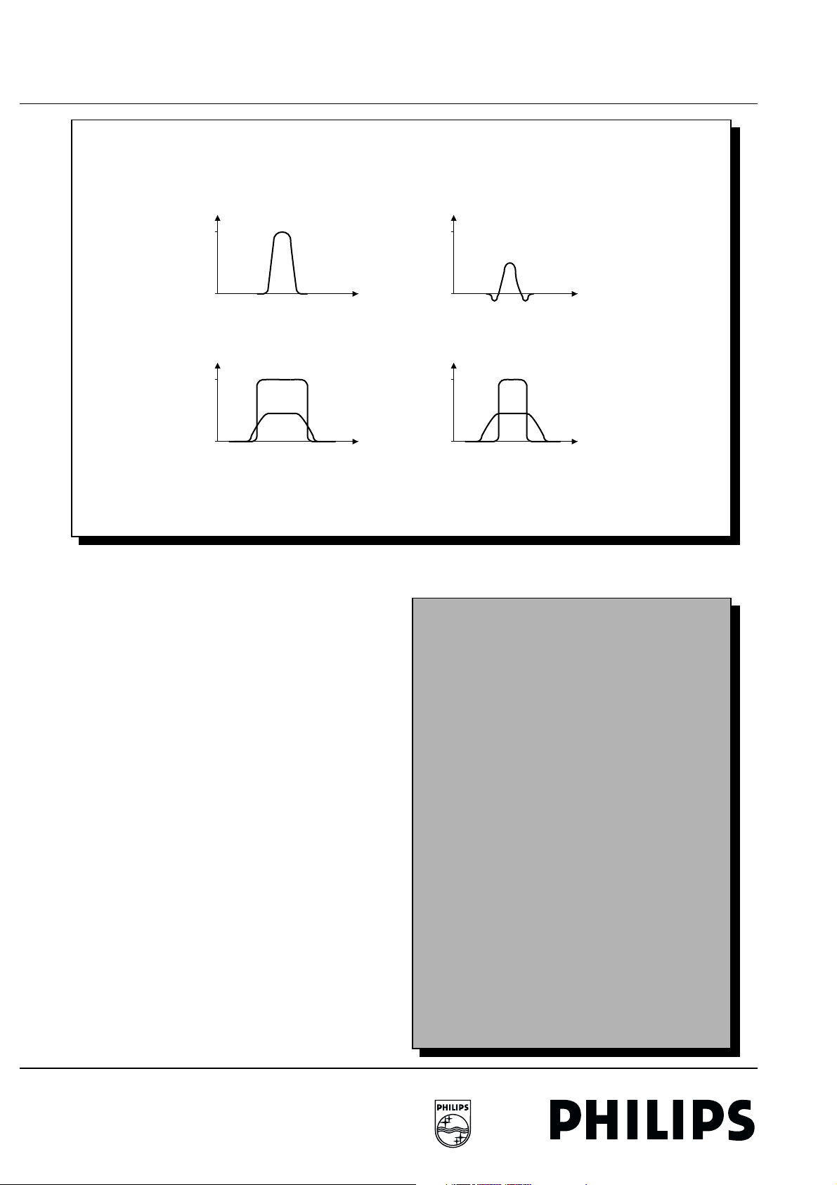
44 6. Video FTV1.9EE Receiver Box
6.7 Video control
LUMINANCE TRANSIENT PROCESSOR
White
Black
White
Black
Max. step improvement / nom. line width Max. step improvement / min. line width
Step improvement
This provision ensures that black-white transitions are made
even steeper. The result of this is that the picture gives a still
sharper impression.
White
Black
PeakingNo Peaking
White
Black
CL 96532069_026.eps
Personal notes
240899
Noise suppression
The LIMERIC in the Feature Box determines the noise level in
the picture and appraises this by means of the noise figure,
which is passed on via I2C to the microprocessor. On the basis
of the noise figure, in addition to the degree of noise
suppression in the LIMERIC and the degree of DNR, the
degree of peaking together with the "steepness" and the
"coring" in the LTP is now also reduced in proportion with the
rise in the noise figure. Because of this, even better noise
suppression can be arranged.
Page 45
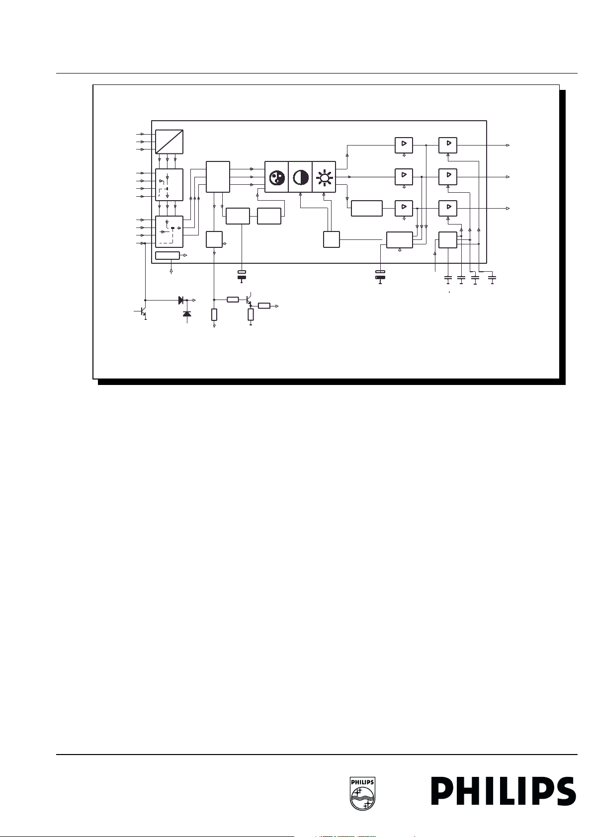
FTV1.9EE Receiver Box 6. Video 45
6.8 Video selection & control (IC7500)
6.8 Video selection & control (IC 7500)
SELECTION & CONTROL
stab.
19 17
2536 2542
330n 100n
DC
c-off
DC
c-off
DC
c-off
off
cut-
TDA4780
to
VCI
24
22
20
21 23 25
2540 2538
100n 100n
CL 96532069_027.eps
240899
Y to scavem
TDA4780
R
G
B
Blue
stretch
adj.
ampl.
white
ampl.
white
ampl.
white
peakwhite
limit I2C
16
2544
measuring
1uF
IC7500
Y
YUV
U86
FBX
V
R
G
PIP
B
F-Bl.
R
G
TXT
B
F-Bl.
txt
kill
from
PIP
RGB
7
10
11
oo
12
o
13
2
3
ooo
4
1
timing
sandc.
6550
7518
F-Bl.
PIP
R
G
B
14
scavem
off
6551
Y
matrix
Y
Y
Y
+DC
26
1k
DC=adj.VCI
r-y
b-y
g-y
Y
adapt.
black
2
C
I
3548
220E
3551
gamma
18
2546
1uF
+
7550
3550
100E
3549
1k
The main functions of the video control IC TDA 4780 are:
• Switching to TXT or OSD.
• Adjustment of:
– Brightness.
– Contrast.
– Saturation.
Switchover and picture controls
The Y, U and V from the Feature box are converted to R, G and
B. This matrix is switched over depending on the colour system,
so that an optimal result is always obtained. With the first RGB
switch the PIP picture can be switched on but this function is not
used in FTV1.9. Via the following RGB switch TXT or OSD can
be switched through.
A number of adjustments are only made on the Y signal so that
Y and three colour difference signals are made from the RGB
in the following matrix. The direct current (DC) on pin 26 can be
adjusted separately. This is used as the soft-clipper
adjustment.
In the adaptive black adjustment (black-stretch), the darkest Yvalue is measured and brought back to black. Because the total
amplitude becomes 15% smaller the contrast is increased (via
the software) by a factor of 1.2 when the black-stretch is
switched on.
The gamma adjustment gives the linear amplification
characteristic a bent shape. A higher gamma adjustment gives
an even more bent characteristic, through which the darkest
passages are given more contrast. This adjustment is coupled
to the brightness adjustment, so that different brightness
adjustments nevertheless result in optimum contrast being
obtained.
Following colour saturation adjustment the signals are once
more converted to R, G and B, following which the contrast and
brightness is adjusted.
Page 46
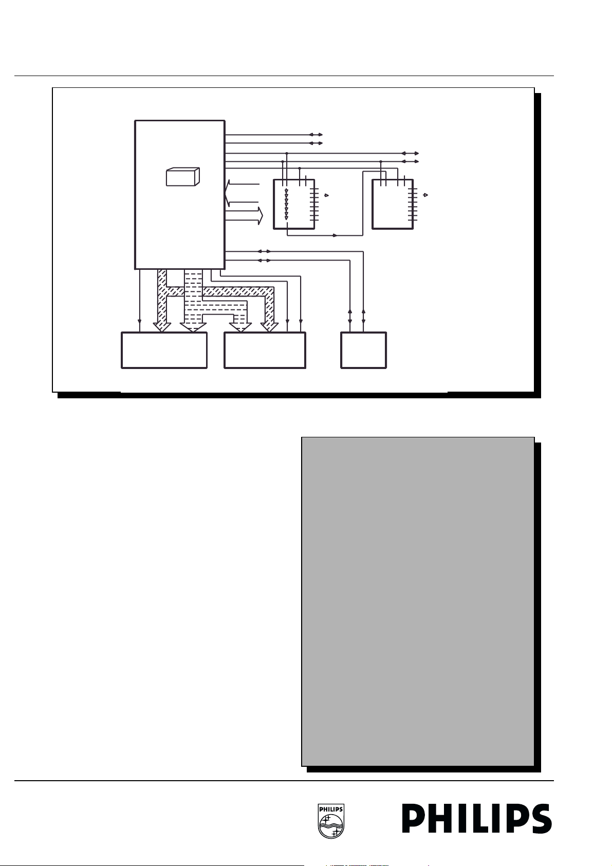
46 7. Control FTV1.9EE Receiver Box
7.1 Control system
7. Control7.1Control system
CONTROL SYSTEM
7202
7200
36
24
OE
ROM
data
data
512k
CPU
adres
20 bits8 bits
adres
50
2
3
4
5
14
outputs
56
12
20
7206
strobe
inputs
interupts
adres
SDA
SCL
I2C-3
data WR
RAM
32k
I2C-F
400kc
SDA
SCL
+
21
I/O
EXP
10
outputs
7204
SDA
SCL
321
I/O
EXP
7213
I2C-S
100kc
+
15153
outputs
uP & control
20
627 5
NVM
16k
7212
CL 96532069_032.eps
240899
The purpose of the control circuits is:
• The control of the various IC's and modules via serial
busses.
• Control of circuits without IC communication via direct
output ports.
• LED control.
The input originates from:
• RC5 operation.
• Local keyboards.
• IC and module status signals via IC.
• Direct input from certain circuits.
• Interrupt lines such stand-by, TXT...
Personal notes
Page 47
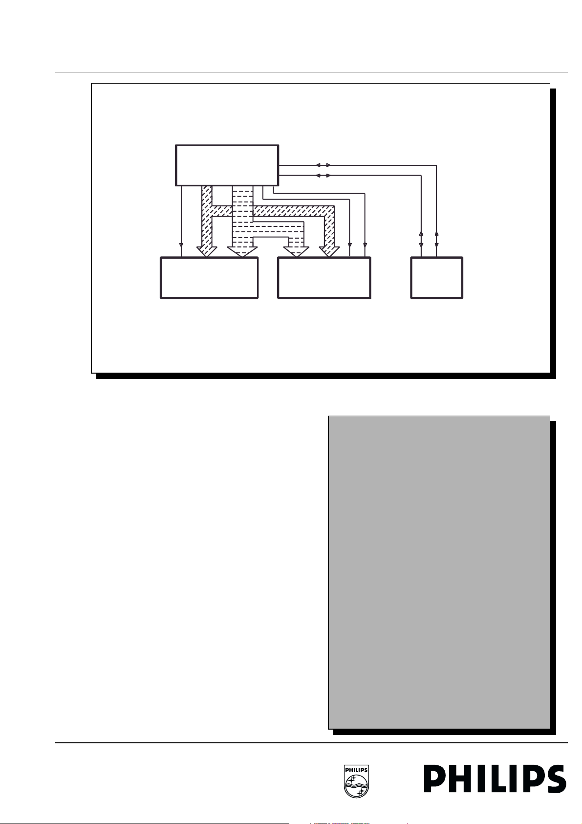
FTV1.9EE Receiver Box 7. Control 47
7.2 Processor, ROM, RAM and EAROM
7.2 Processor, ROM, RAM a nd EAROM
7200
CPU
data
36
adres
20 bits8 bits
56
12
20
50
I2C-3
SDA
SCL
24
data
OE
adres
adres
ROM
512k
7202
Operating control is built up around a 16-bit microprocessor
with an internal interface for ROM, RAM and direct input and
output ports. Speedy interruption of the program can be
achieved via the interrupt lines.
There are three IC busses:
• The "SLOW" has a clock frequency of 100 kHz.
• The "FAST" operates at 400 kHz.
• The third bus is only used for the EAROM (Non Volatile
Memory).
The software is located in the 512 kByte ROM, IC7202. Use of
a 1 MByte ROM is also possible. If the output enable line on pin
24 is low 8 data bits are placed on the data bus.
The working memory consists of a 32 kByte RAM, IC7206. The
8 data bits are read out if pin 20 is low. If pin 27 is low the RAM
can be written to. All temporary changes to parameters of the
set in operation are stored here. The contents are lost when the
set is switched off.
The Non Volatile Memory, IC7212, contains the pre-set and
program data of the transmitters, option codes and sound and
picture adjustments, etc. The EAROM used has a capacity of 2
kByte (16 kBit).
7206
20
data WR
RAM
32k
Personal notes
627 5
NVM
16k
7212
CL 96532069_033.eps
120799
Page 48
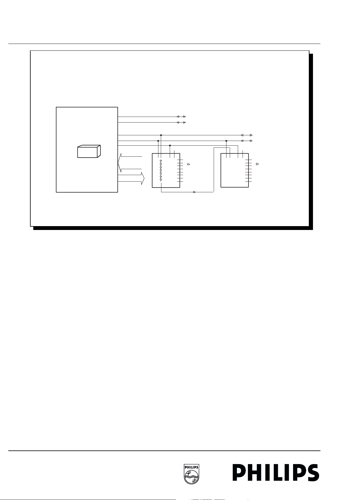
48 7. Control FTV1.9EE Receiver Box
7.3 The output interface
7.3 The output interface
OUTPUT INTERFACE
7200
CPU
2
3
4
5
14
SDA
SCL
strobe
inputs
interupts
outputs
Because the microprocessor does not have enough outputs, 2
external output expanders are used. IC7204 and IC7213
provide the extra outputs (16). These IC's, shift registers of the
type HEF4094, are controlled by the IC bus. As the HEF4094
IC's do not support IC communication, the use of an extra
strobe pulse is necessary. When the strobe on pin 1 becomes
high the data bits on the SDA line will read into the buffers. After
16 clock pulses (SCL) each register in both IC's contain a data
bit from the serial sequence. The output enable pin 15 is
permanently high so that the bits are available on the outputs.
The microprocessor can receive interrupts from TXT, the I/O
panel, stand-by and. There are three IC busses and an RC5
input. The lines FRNT_01 to FRNT_05 are used for LED control
and control keys.
I2C-F
400kc
SDA
SCL
+
21
I/O
EXP
10
outputs
7204
321
I/O
EXP
7213
I2C-S
100kc
+
15153
outputs
CL 96532069_034.eps
240899
Outputs:
• Sound mute (SOUND_ENABLE)
• Strobe output expanders HEF4094 (STROBE)
• Comb filter colour system selection (SYS1 and SYS2)
• SECAM notch filter on (SEC_NOTCH)
• Service LED (IR_LED)
• Stand-by (STBY)
Inputs:
• RC5 receiver (RECEI_RC5)
• Local keyboard and LED's (output) (FRNT_01 to 05)
• Video recognition Front-End (STR_FE)
• Power on Reset pulse (POR1)
• Protection line (PROT)
• Interrupt Source Select (IRQ_SS)
• Interrupt TXT (IRQ_TXT)
• Interrupt D2B/RGB kill (IRQ_D2B/RGB_KILL)
Page 49
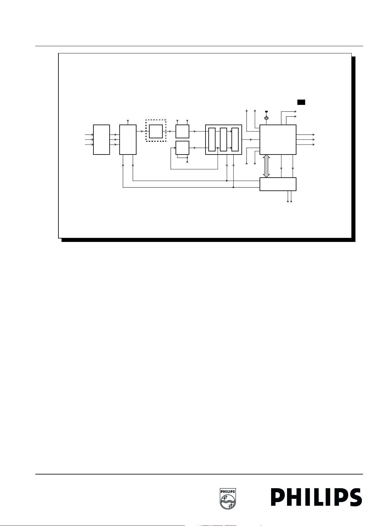
FTV1.9EE Receiver Box 8. Featurebox 49
8. Featurebox
BLOCK DIAGRAM FEATURE BOX 4
(NATURAL MOTION)
U50
V50
Y50
SWCK SWCK SRCK
7440/7441 74507447
PRE
FILTER
FRONTIC
ADC
12 Bit
PAL PLUS
AI
PANEL
UP CL
UP DA
7445
12 Bit
7446
MEM1
3MBIT
MEM2
3MBIT
SRCK
The feature box 4 (also called FBX4) is the successor of the
digital scan (FBX3) box.
The Y,U,V signals are converted to digital information within the
the Featurebox - FBX4. The line frequency is doubled to a line
frequency of 32kHz. The frame frequency remains the same.
The PDP can not handle frequency above 72Hz.
In case of a 60 Hz signal, for example NTSC-M, these 60 Hz
based signals are not converted to 120 Hz but to a 60 Hz signal
without interlacing. This means that the line frequency is 2fh but
the frame frequency remains 60 Hz.
The Featurebox also contains extra digital features as Natural
Motion, zoom-function and noise reduction.
Also the AARA Automatic Aspect Ratio Adaptation is
performed in the feature box.
After storing, processing and reading the digital information is
converted back to analogue Y, U and V information, but then
based on a 2fh line frequency. The Y, U and V are fed to the
outputs for further processing.
The Feature-box 4 can be divided in the following blocks:
1. Functions of the FBX4.
1. Introduction.
2. Natural motion.
2. Block diagram.
3. FRONTIC.
4. AI panel.
1. LIMERIC.
2. SMARTIC and Autoformat AARA.
3. PANIC.
5. MELZONIC.
12 Bit
A
12 Bit
B
6. Eco-BENDIC.
D
N
R
C
MELZONIC
Motion
Estimation
D
Vert.Zoom
Progres.Scan
12 Bits
VA HA
32MC16MC
12MC
ECO
BENDIC
XTAL
Data
Address
MICROPROCESSOR
CL 96532069_019.eps
M2
VD
HD
Y100
U100
V100
RESET
7505
I2C
240799
Page 50
50 8. Featurebox FTV1.9EE Receiver Box
8.1 Functions of the FBX4:
8.1 Functions of the FBX4:
The functions within the FBX4 are listed below and can be
found more in details in the next paragraphs:
• Motion-vector compensated field rate upconversion (50 to
100 Hz) AABB.
• Motion estimation.
• Motion-vector compensated line flicker reduction AB`A`B.
• Movie fast detection (LFR switch off for cinematic picture).
• Noise reduction DNR.
• Variable vertical zoom.
• Digital luminance peaking.
• DC frame.
• Horizontal zoom function.
• PALplus possible.
Introduction
The Feature Box 4 is based on the Feature Box 3, but in
addition this FBX also has the possibility allowing movements
to flow more freely, called "Natural Motion". This function is also
known as motion estimation and compensation. For this
function the PROZONIC-IC (PRogressive scan, ZOom and
Noise reduction IC) from Feature Box 3 is replaced with a new
IC called MELZONIC (Motion Estimation, Line flicker, ZOom
and Noise reduction IC).
Personal notes
Natural Motion
The basis for the picture not following naturally is the fact that a
TV picture only changes 50 times a second. That means that on
movement the position on the screen is only changed once
every 1/50th of a second (Raster A1, Raster B1, Raster A2,
etc.). When displayed on a 100 Hz TV all pictures are displayed
twice, whereby the 2 successive pictures remain the same (A1,
A1, B1, B1), so the number of actual positional changes
therefore also remains the same. The natural motion" function
will generate a third picture between the two existing pictures,
which will move the position of a moving object to such an
extent that it is located between the position of the object in the
first picture and position of the object in the second picture.
The result is that on a 100 Hz display moving objects in the
intermediary pictures (A1', B1') have a modified position in
relation to the original pictures (A1, B1), with motion appearing
more natural as a result.
When displaying cinema films (that originally only showed 24
Frames per second) the picture contents only changes 25 times
a second. This means that every 4 frames in a 100 Hz picture
have the same picture content. In this case natural motion once
again generates intermediary pictures, resulting in movements
appearing to flow more smoothly.
Page 51
FTV1.9EE Receiver Box 8. Featurebox 51
8.2 Block diagram
8.2 Block diagram
The YUV signal is offered to 3 low-pass filters that cut off the
highest frequencies in order to avoid aliasing. The signals are
offered to the FRONTIC (IC7440). This IC contains a triple A/D
converter and a sample function. The sample rate is
determined by the used horizontal zoom mode.
Once the signal has been digitised the information is processed
by the Al (Artificial Intelligence) panel and eventually by the
PALplus module.
The 12 bit information is written into MEM1. Memory 1 and 2
both consist of 3 memories of 1 MBIT, of which 2 memories are
used for the Y signal and 1 memory for the U and V signal.
The write clock runs at 16 MHz and read clock at 32 MHz.
The 100 Hz YUV signal is offered to the MELZONIC (IC7447).
By using both MEM2 and MEM1 the MELZONIC has two
complete frames at its disposal. With this information the
MELZONIC can perform the following functions:
• DNR or Dynamic Noise Reduction.
• LFR or Line Flicker Reduction.
• Progressive Scan
• Zoom function, (vertical)
• Motion estimation
Via the signal processing in the MELZONIC the data is offered
to the Eco-BENDIC.
The Eco-BENDIC operates with an external 12 MHz crystal. All
clock signals are generated in the Eco-BENDIC. 50/100 Hz
conversion is performed with one clock system. The read clock
is divided by 2 internally and used as the write clock. The EcoBENDIC is controlled by the up (IC7505) via address/data lines.
The display clock is locked with the BK50 pulse (burst key 50
Hz) by means of an internal PLL. The Eco-BENDIC is
synchronised using line and frame pulses originating from the
sync IC, this IC Is located on the SSP (TDA9144).
The FBX-up is connected with the main up via I2C, and with the
Eco-BENDIC via an address/data bus. The up receives a reset
impulse on start up.
The YUV signal is offered to the video control IC via 3 filterstages.
Personal notes
Page 52
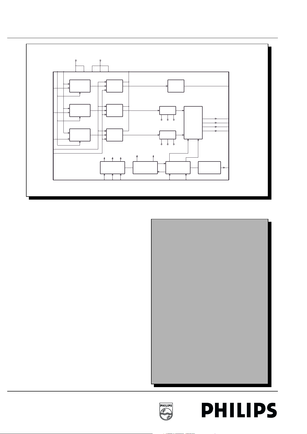
52 8. Featurebox FTV1.9EE Receiver Box
8.3 FRONTIC-IC
8.3 FRONTIC-IC
INY
38
INU
INV
CREFH
CREFL
+5V DIG
CLREF CLAMP
27 20
35
32
29
28
CLAMP
CLAMP
CLAMP
+5V ANALOG
31925
3734 16
8 BIT
A/D
8 BIT
A/D
8 BIT
A/D
SERIAL
INTERFACE
41 40
UPDA
42
UPCL V50
FRONT IC
CLOCK
ON/OFF
NOTCH
DELTA
DTO
TDA8753
HOLD
HOLD
SIGN
LPF
INTERPOL.
DOWNSAMPL.
RESET
DELTA
INTERPOL.
DOWNSAMPL.
RESET
DELTA
MEMORY
INTERFACE
19 18
HREF WE
U AND V
FORMATTER
IC7440
11
12
13
14
DELAY
CL 96532069_039.eps
240899
17
MSB=Y7
1
Y7
2
3
4
5
6
7
Y0
8
U1
U0
V1
V0
WEO
The FRONTIC (FRONT-IC) contains three 8-bit D/A-converters
and provides also the possibility for a horizontal zoom-mode
(only used in case of no AI-panel).
The analogue 50 Hz Y, U and V-signal is fed to the three 8 bit
flash-A/D-converters.
On every clock impulse of 16 MHz a sample from the input is
digitised.
The 8 bit Y, U and V information is fed to the digital sample rate
converters via filters.
These converters can vary the number of samples by holding
samples for longer and thereby disregarding others.
The Y-signal from the A/D converter remain still 8 bit; the U and
V-signals are subsequently compressed into a total of 4 bits /
16 MHz.
Personal notes
Page 53
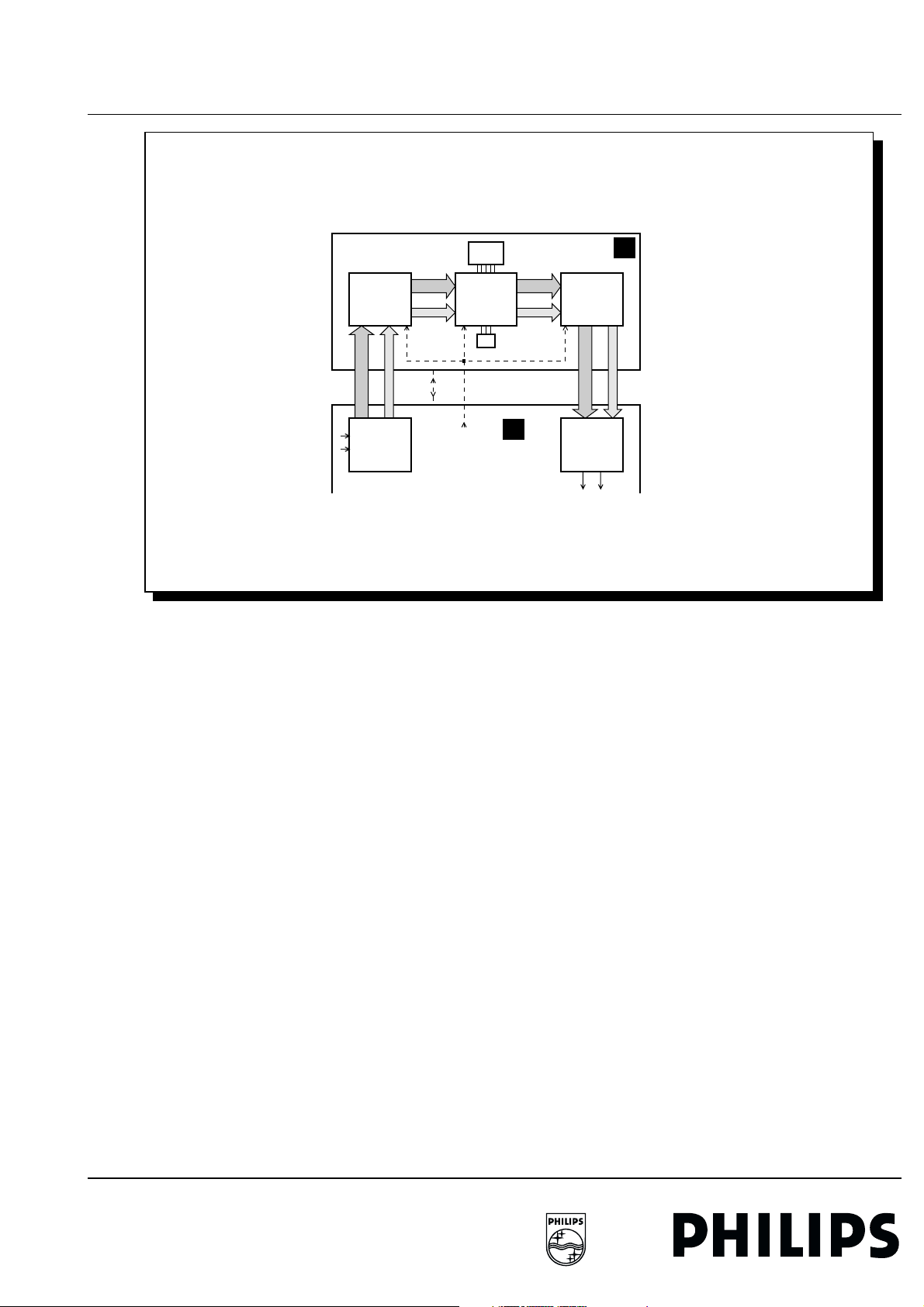
FTV1.9EE Receiver Box 8. Featurebox 53
8.4 AI panel (PALplus - optional)
8.4 AI panel (PALplus - optional)
AI-PANEL (PAL PLUS)
AI-Panel
7007
Subt.
7006 70107008
Y
Limeric Smartic Panic
U - V
RAM
µP
Y
U - V
7009
N
U
8b 4b 8b 4b
Y
Frontic
A/D conv.
V
timing
Snertbus
7440/7441
FBX
For picture improvements the Feature Box can be expanded
with an Al panel (Artificial Intelligence).
This is a small add-on board which can contain the LIMERIC
(Llne MEmory noise Reduction IC) and/or SMARTIC (Subtitle
Movement and ARTifical Intelligence IC) and/or PANIC
(PANorama IC) function.
All 3 IC's are described in short. The Al print receives the digital
8 bit Y signal and the 4 bit U/V signal that originate from this
FRONTIC in the FBX. The three IC's are driven by the so called
"SNERTBUS" In the FBX, which also supplies and receives a
number of timing and clock signals from the Al-panel.
The memory in the FBX receives the signals generated.
LIMERIC:
Noise reduction
LIMERIC stands for Llne MEmory noise Reduction IC. This IC
takes care for noise reduction on line level. As noise consists of
unpredictable peaks which are difficult to filter out of the picture
content.
The following constraints should be mentioned:
• Noise has no relation with the pixel next to it. Picture
information normally does have such a relation unless there
is a very rapid changeover.
• Noise has no relation with the previous and the following
picture line. Picture information normally has this relation
(especially when there is no relation with the pixels next to
it).
U
Y
V
M
Mem.
50 - 100Hz
CL 96532069_021.eps
240899
• Noise has no relation with the following and the previous
frames. Picture information normally does have this relation
unless there are fast movements.
• With these 3 criteria's noise can be recognised.
Operation
The LIMERIC gets the digital video signal, which will be split up
in chrominance and luminance. From the picture blocks are
selected in which no movements appear (e.g. a grey block in
the picture); in these blocks it is the easiest to recognise noise.
For these blocks the amount of noise is determined.
This amount is quantified in a value. By making such a value
continuously frame after frame, a factor can be extracted which
is called the noise-factor. With this factor the noise filter can be
adjusted. This can be done both with the DNR
(Dynamic Noise Reduction) in the MELZONIC and as linenoise reduction function in the LIMERIC:
• In case of an noiseless picture both the LIMERIC noise
reduction as the DNR is switched off
• In case of a weak noise the DNR is switched on at a level
which is determined by the noise-factor, and the LIMERIC
noise reduction is switched off.
• In case of medium noise the DNR is switched to the
maximum level and the noise reduction in the LIMERIC
slowly starts.
• In case of strong noise both the DNR and the LIMERIC are
switched on.
Page 54
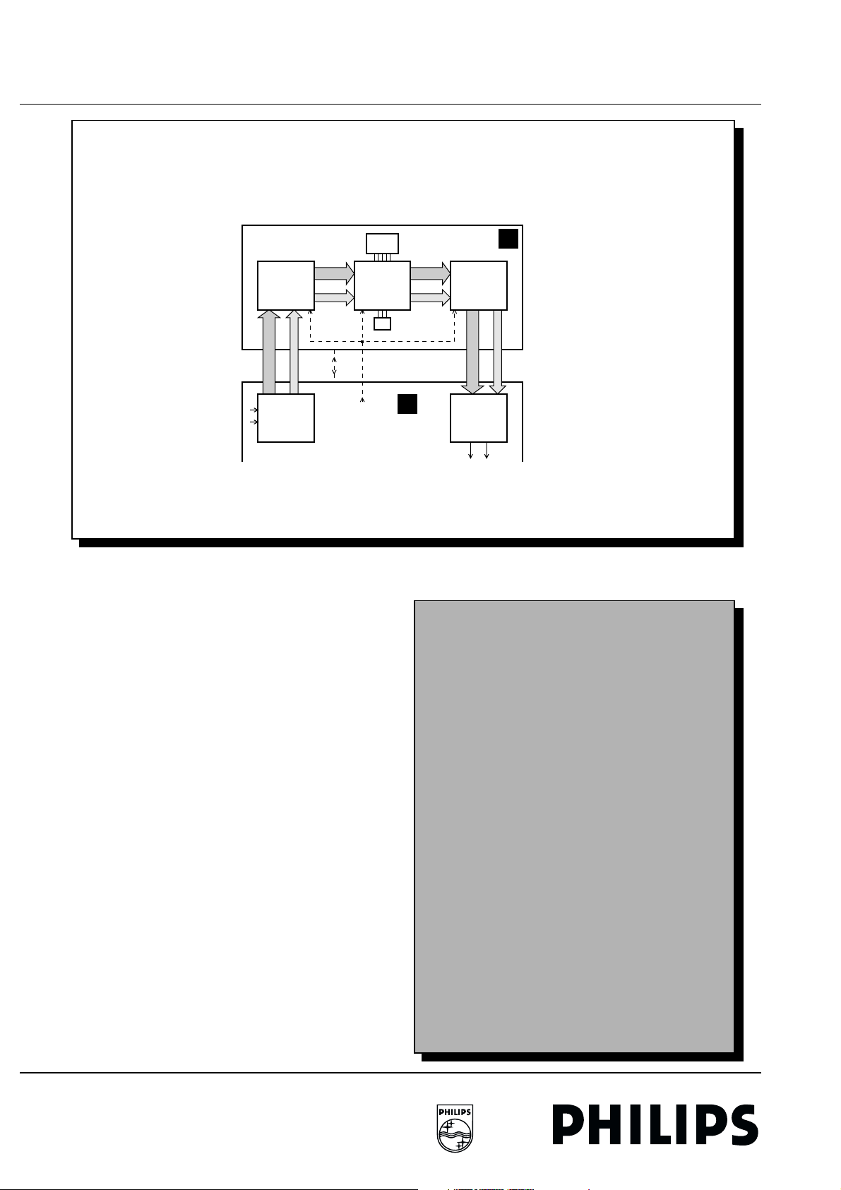
54 8. Featurebox FTV1.9EE Receiver Box
8.4 AI panel (PALplus - optional)
AI-PANEL (PAL PLUS)
AI-Panel
7007
Subt.
7006 70107008
Y
Limeric Smartic Panic
U - V
RAM
µP
Y
U - V
7009
N
U
8b 4b 8b 4b
Y
Frontic
A/D conv.
V
timing
Snertbus
7440/7441
FBX
Noise reduction in the LIMERIC
DNR at line level is done by the LIMERIC. In the LIMERIC IC
every pixel is compared with 5 pixels from the previous line and
with 3 pixels from the same line. In case a pixel is recognised
as noise, by then an average is calculated of the surrounding
pixels. This calculated pixel is inserted on that spot.
SMARTIC
Purpose
The SMARTIC IC (Subtitle Movement and ARTifical
Intelligence IC) is used as a digital dynamic contrast adjustment
and replaces the previous analogue black stretch. The purpose
of this adjustment is to increase the impression of contrast. The
subtle movement feature is not used .The SMARTIC has its
own processor. In case subtitle shift" is applied the circuit also
contains extra RAM memory.
Also the Auto-Format-function is realised with the SMARTIC.
This solution is completely independent of the main software.
The SMARTIC detects which percentage of the total active
picture is black for a longer time.
Based on this information a correct expanding factor is
calculated and applied.
AARA (Auto Aspect Ratio) has to be switched off in case of DW/
multi PIP or PALplus by the software.
Y
M
Mem.
50 - 100Hz
CL 96532069_021.eps
Personal notes
U
V
240899
Page 55
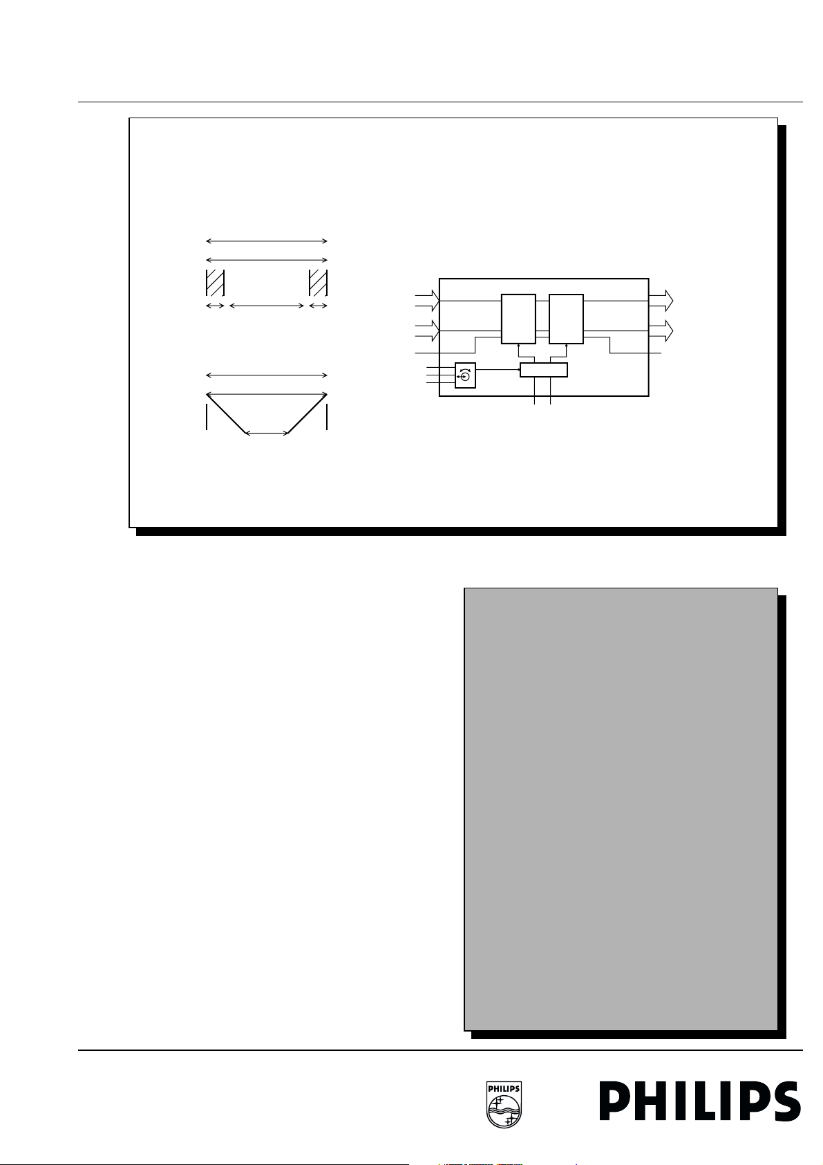
FTV1.9EE Receiver Box 8. Featurebox 55
8.4 AI panel (PALplus - optional)
PANIC
64 µs
25
Samples
200 Samples
150
Samples
Fig. a.
64 µs
200 Samples
50
Samples
25
Samples
4/3 DISPLAY
IN 16/9 SET
ZOOM
37
Y
44
1
UV
4
7
WE
34
DA
35
CL
36
RST
LINEAR
ZOOM
ZOOM CONTROL
SUPERWIDE
ZOOM
CLK-32CLK-16
315
22
Y
29
18
UV
21
17
Fig. b.
PANIC
The purpose of the PANIC (PANorama IC) is to achieve a
horizontal zoom function by using of "sample and insert".
The vertical zoom function is realised by the MELZONIC.
• 4/3 displayed on a 16/9 screen (fig. a)
The PANIC insert in every line 50 black samples; the content of
the picture is compressed by exchange of 4 samples of the
original picture content by 3 "new" samples (algor. operation).
The sampling frequency of 16 MHz is high enough so that no
lost of resolution is visible.
• Super-Wide
The PANIC provides a new calculation of the samples; on the
left and the right side of the picture new samples are generated
and inserted by the PANIC; in the middle of the picture the
original value of the samples remain.
• ZOOM function
The zoom function is realised by using only 50, 33 or 25 % of a
line and insert one, two or three samples in the line by using a
arithmetic operation. The complete line is a product of adding
the new samples with the samples generated by the
interpolation. Because of this fact the horizontal resolution
decreases.
Also the vertical resolution decreases by the same factor (see
fig b).
Personal notes
CL 96532069_024.eps
040899
Page 56
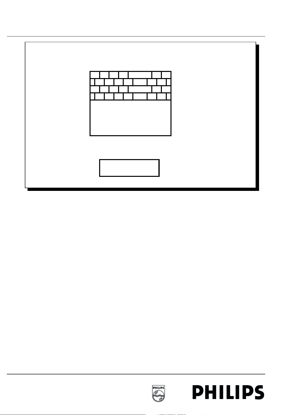
56 8. Featurebox FTV1.9EE Receiver Box
8.5 MELZONIC
8.5 MELZONIC
MELZONIC
Max. 107 blocks
1 3 5 7 105 107
2468 104106
3 5 7 105 107
1
2468 104106
Max. 74 blocks
16 Pixels
xxxxxxxxxxxxxxxx
4 Lines
x
x
x
Motion estimation
Motion estimation and DNR at frame level is performed by
using the MELZONIC (SAA4991).
In addition this IC also contains all the features of the
PROZONIC.
Principle
A frame is split up into different blocks. 1 block consists of 16
pixels and is 4 lines high. A frame therefore consists of
approximately (horizontal) 107 blocks x (vertical) 74 blocks = +/
- 7918 blocks.
The value of every block is determined in a frame. A search is
subsequently made in the adjacent blocks in the following
frame for the block with the same contents. Following
comparison a vector is determined that indicates the
movement of that block.
After the comparison of 2 complete frames, these vectors are
then used to determine the content of the 2nd and 3rd frame.
This results in two new frames being made, the motionless
parts of which remain in the same position, with the moving
parts being shifted into a position located between the position
of that part on the first and fourth frame.
As is apparent from the above, natural motion works extremely
effectively on objects that move over the screen with a speed of
+/- 16 pixels per 20 ms.
This is equivalent to the movement of a specific object from left
to right across the screen in +/- 2 sec.
1 Block
CL 96532069_036.eps
240899
Natural motion is therefore also especially effective on cinema
(movie) pictures , considering the limited number of pictures per
second (25 frames a second).
The block diagram of the MELZONIC IC is internally very
similar to that of the PROZONIC IC, which is logical considering
that many functions are the same. Two areas have been added
for natural motion:
• Motion estimation, where movements are estimated;
• Motion compensation, which adjusts the pictures. This
adjustment is performed in real time.
Page 57
FTV1.9EE Receiver Box 8. Featurebox 57
8.6 ECO-BENDIC
8.6 E CO-BENDIC
The 12 bit signal originated from the MELZONIC is offered to
the ECO-BENDIC (Back-END-IC).
All clock-signals are generated by the ECO-BENDIC.
The IC is controlled by the microprocessor via address/data
lines and delivers the digital processed YUV-signals to the
IC7580 (TDA9177).
Personal notes
Page 58
58 9. Double window FTV1.9EE Receiver Box
9.1 General:
9. Double window9.1Genera l:
The Double-Window-module is build up around the PIPO
(Picture In Picture Out) processor SAA 9077.
The circuit is able to process PIP, POP or DW-signals, but in
FTV 1.9 only the DW-function is used.
Personal notes
Page 59
FTV1.9EE Receiver Box 9. Double window 59
9.2 Introduction
9.2 Introduction
The Video DualScreen picture consists of 2 sections of the
same size:
• The left-hand section is the main picture originating from the
main tuner or from RGB, CVBS or SVHS signals from
external sources.
• The right-hand section is the sub-image originating from the
2nd tuner or from CVBS or SVHS signals (no RGB signals)
from external sources. The video decoding for the subimage takes place on the Video DualScreen module and
makes no use of the COMB filter and LTP. The result is that
the picture quality of the sub-image is generally a little less
than that of the main picture.
• 1fh RGB signals from externals can not be used in the sub
signal part because the Eco Euro I/O has only 1 RGB
output.
• Multi PIP (Active Mosaic) and photo-finish are made in the
Double Window module.
• The Double Window YUV signals are inserted on (1fh
basis).
• DW can not be combined with a VGA main picture.
Personal notes
Page 60
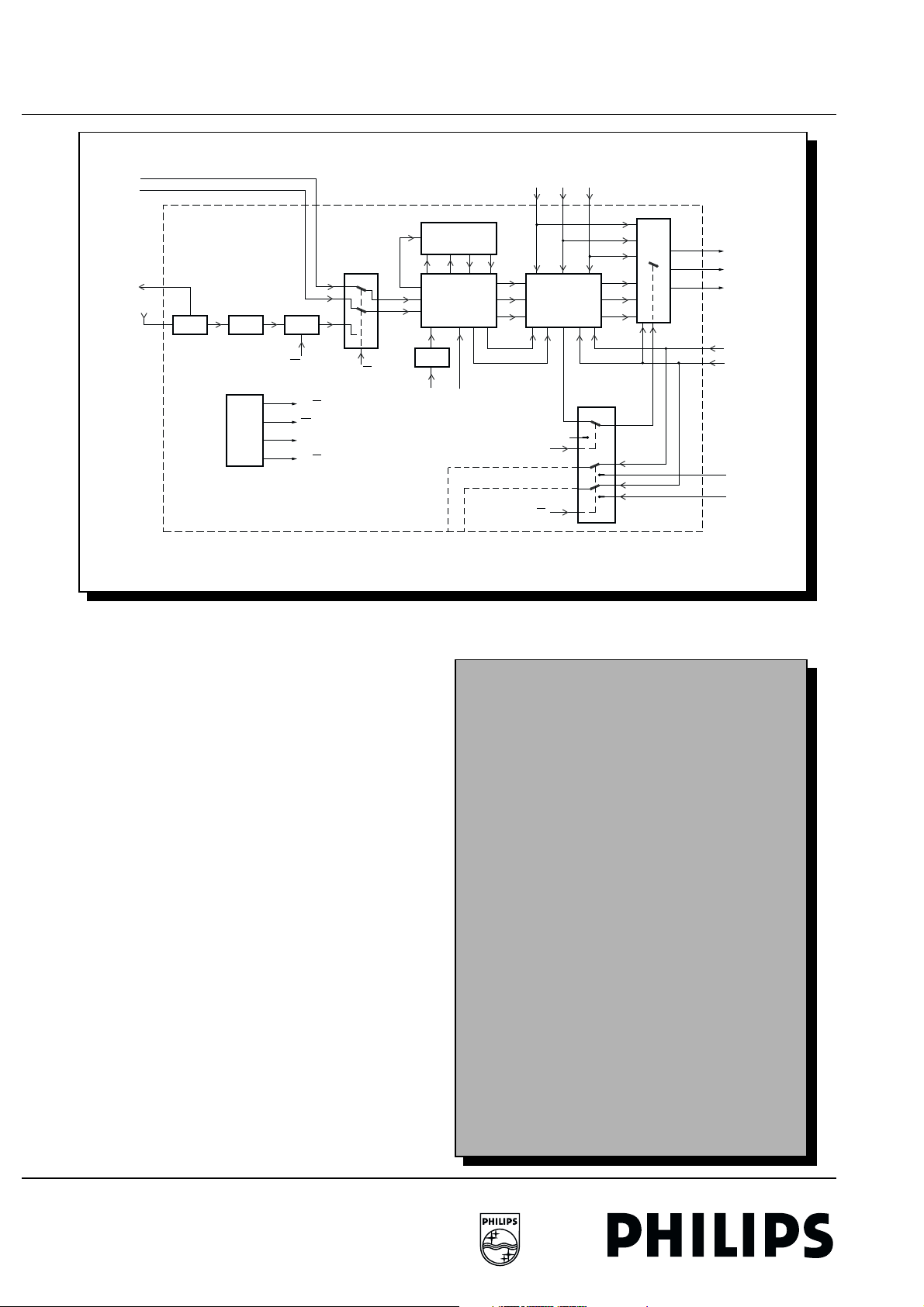
60 9. Double window FTV1.9EE Receiver Box
9.3 Block diagram Video Part
9.3 Block diagram Video Part
C_DW
CVBS/Y_DW
TO MAIN
TUNER
BLOCK DIAGRAM VIDEO
PIPO
SAB9077
+5V
VTXT
H_TXT
HA
74HC4053
Y_MAIN
U_MAIN
V_MAIN
DY
DU
DV
VA
TDA8601
Y_DW
U_DW
V_DW
DFB2HA
VA
VD
HA
HDISP
CL 96532069_028.eps
240899
SC 1fH DW
74HC4053
C
RF
RF IF CVBS
SPLITTER
TUNER
PCF8574T
I/O
EXPANDER
TDA9600
TDA9802
POS/NEG
EXT/INT
POS/NEG
FBLK
TXT/EXT
CVBS/Y
EXT/INT
PAL DELAY LINE
TDA4665
-(B-Y) -(R-Y) U V
COLOUR
DECODING
TDA9143
FB
3X LPF
RGB_DW
Hdisp TXT
MY MU MV
SY
SU
SV
SPHsync
SPVsync
DFB1
FBLK
TXT/EXT
The following blocks can be distinguished on the Video Dual
Screen module:
• PLL tuner - UV1216D which is driven via I2C-bus
• TDA980x is used for IF demodulation.
• The PCF8574AT controller IC9N is used in order to set the
switching signals from the IF demodulator into the correct
mode. Via a source selector IC9L - 74HC4053 a selection is
made between TUN_CVBS (from the Video Dual Screen
tuner) or CVBS PIP (from the I/O-Panel on the SSP). At the
same time this IC9L can be used to select between CVBSPIP or YC-PIP. The Y/CVBS-PIP or CVBS TUNER signal
and the C-PIP signal are fed to the TDA9143 IC9J on the
Video DualScreen module. Together with the delay line
IC9K - TDA4665 the CVBS or SVHS signal is converted
here to the SUB-YUV signals together with the sync signals
SPHsync and SPVsync.
• The RGB-TXT inputs of this TDA9143 are not used here.
The sub-YUV signals (SY, SU, and SV) together with their
sync. signals SPVsync and SPHsync and the Main-YUV
signals (MU, MY, MV) with their sync signals HA = SC_1FH
= DPHsync and VA = DPVsync are placed next to each
other in the PIPO (Picture In Picture Out) IC9A SAB9077.
• The RAM IC9E is used as the memory. The output of the
SAB9077 DW-YUV signals (DY, DU and DV) are fed
directly to the fast switching IC IC9M which is controlled by
the I/O-expander PCF8574T
• The output of the TDA8601 is offered to the feature box
FBX4 to convert the signals to 2fh and to process feature
like natural motion; DNR etc.
Personal notes
Page 61
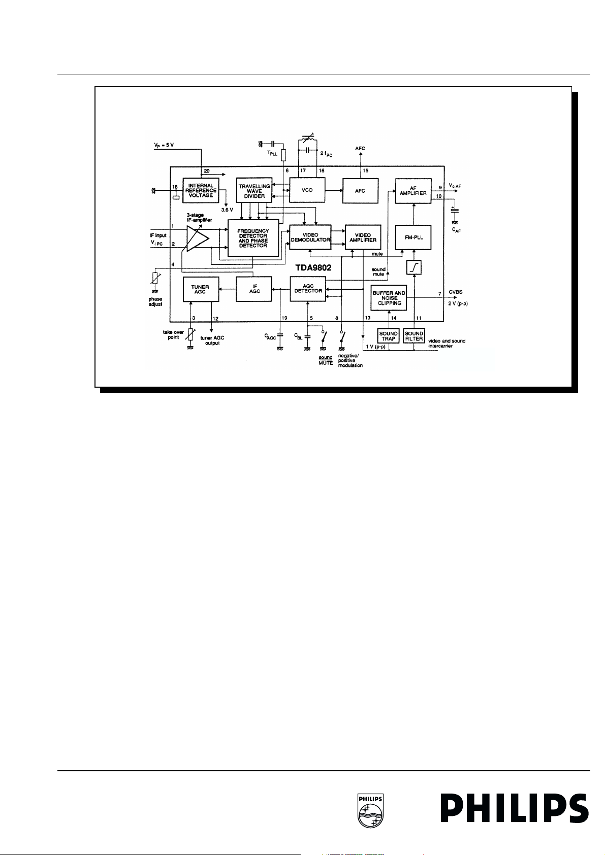
FTV1.9EE Receiver Box 9. Double window 61
9.3 Block diagram Video Part
VIF-DEMODULATOR
Detailed description
The sub tuner on the DW-module receives his input signal from
the splitter located at the main tuner on the SSP.
The sub-tuner is I2C controlled and offers his IF-output signal
via a filter stage to the input (pin 2) of the IF-IC 9G TDA9802.
The TDA9802 is a multi standard VIF-demodulator which can
process pos. and neg. modulation.
It contents a 3-stage amplifier; an alignment free FM-PLL
detector stage, AGC control and an AFC-loop.
The CVBS output signal of the IF-stage is fed to the video
switching IC 9L (MC14053).
By using the pins 9, 10 and 11 a choice is made between the
internal and external signal.
The Double Window module sub signal part can handle off-air,
CVBS and Y/C signals (video only, NO SOUND!!).
1fh RGB signals from externals cannot be used in the sub
signal part because the Eco Euro I/O has only 1 RGB output.
SourceMainSub
Off-air CVBSYesYes
Ext. CVBS, Y/C, YUVYesYes
1Fh YesNo
The output signal is offered via the pins 4 and 15 to the colour
decoding IC TDA 9143; pin 26 receives the Y/CVBS; pin 25 the
C-signal. The function of the TDA 9143 is identical with the
TDA9144 on the SSP but no helper-line detection (for PALplus)
is integrated. 1fh RGB from a TXT decoder can in principle also
be handled by the sub signal part. However this is not used in
FTV1.9.
CL 96532069_008.eps
240899
For PAL sets a colour delay IC TDA4665T works in combination
with the chroma-IC.
The SUB_YUV-signals from the TDA9143 and the MAIN_YUV
signals are offered to the PIPO-IC SAB 9077 which processes
double window and multi PIP.
The Main YUV signal is routed to the DW module via the S93
YUV connector after the TDA9144. It can either be routed back
to the SSP unaffectedly or it can be compressed and combined
with a compressed Sub signal (second signal from the IO
module or 2nd tuner) to form the double window picture.
The output-signals of the PIPO-IC (pin 83,88,90) are delivered
to the fast video switch TDA8601T / IC 9M which is controlled
by the main up via pin 5; by that a decision whether main or
DW-signal will be displayed is determined.
Double-Window restrictions
The double window panels has several restrictions which are:
• DW can not be combined with VGA because DW is already
inserted in the main picture before the feature box.
• DW can not be used for TV/TXT combination because the
readability for TXT is low if it is compressed by the DW
module, especially because of the new user interface that is
used for FTV1.9.
• TXT can be displayed in mixed mode over (on top of) the
DW picture.
• The base band signal of the second tuner can not be
switched to the external outputs. Because of that it is not
Page 62
62 9. Double window FTV1.9EE Receiver Box
9.3 Block diagram Video Part
possible to decode scrambled signals in the DW Sub
picture.
Personal notes
Page 63
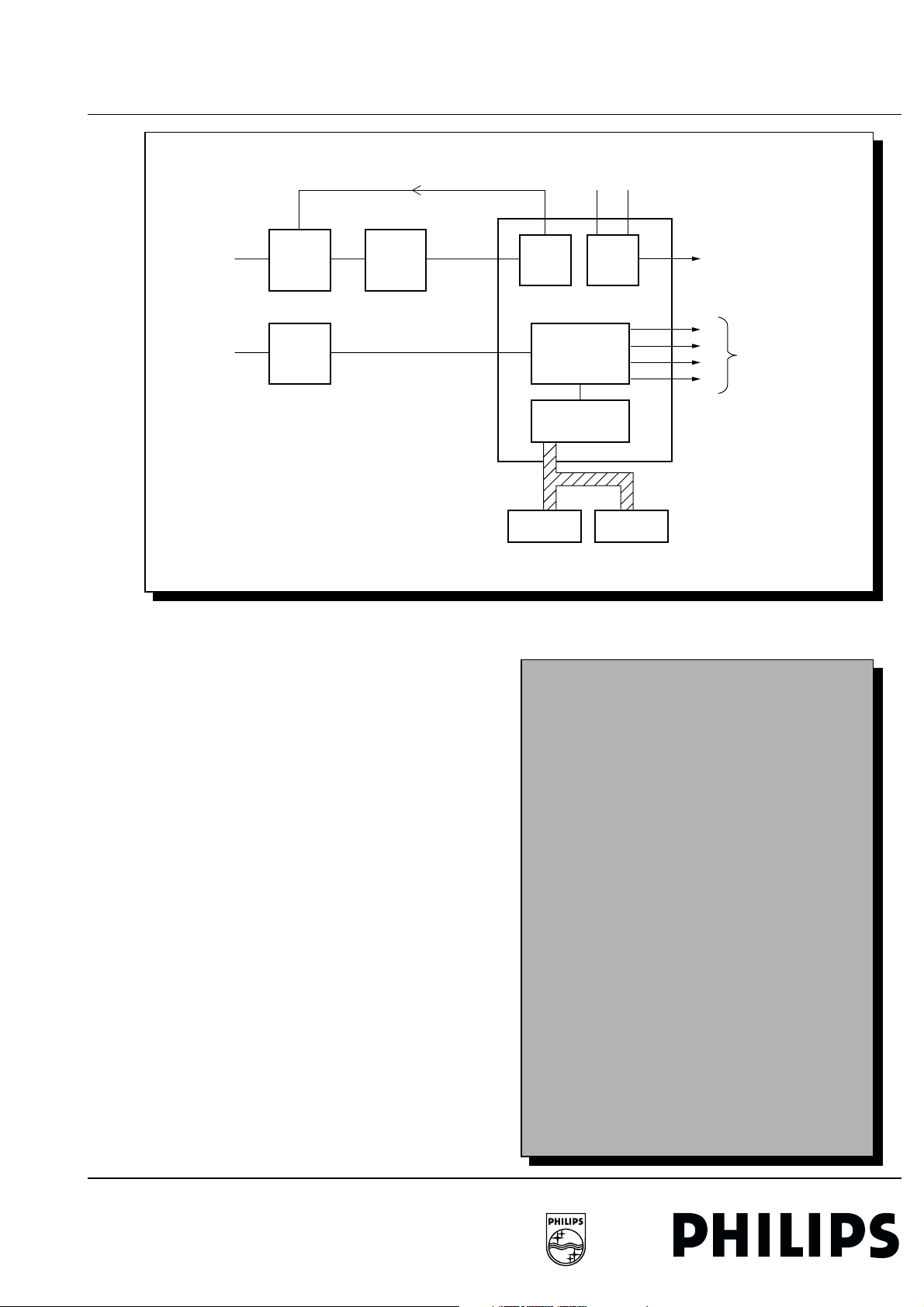
FTV1.9EE Receiver Box 10. Teletext 63
10.1 General
10. Teletext10.1General
TXT-PANEL
IC7051
SDA5270
SDA SCL
33736
HDISP
CVBS
14
27
IC7250
SAA5231
PLL
VIP
13
15
VCO
The teletext decoder is built up around the teletext processor
SAA5278 and a memory IC. All TXT circuits (except the page
memory) are located in the SAA5278.
A 27 MHz crystal oscillator around PLL IC7050 provides the
timing for all circuits in the IC. The 27 MHz clock is fed to the
TXT IC via pin 6.
The CVBS signal is connected to pin 27 of the Video Input
Processor IC7250. The teletext data is then fed to pin 52 of the
TXT-processor.
The signal is offered to the memory via the DRAM interface.
The TXT information is written into the external memory
The voltage on pin 1 and pin 68 determine whether 1 or 2
external memories are present. One memory of 1Mb can
contain 150 to 200 pages, depending on the text content.
The teletext IC contains an internal memory for 32 pages, which
are stored as full pages. In this manner certain pages can be
displayed extremely quickly (e.g. subtitles).
The requested TXT page is read from memory and converted
into ASCII codes. The pages are converted to RGB signals via
a character generator and transmitted via pins 24, 28 and 29
respectively.
The Fast Blanking is output on pin 31.
The colour look-up table (CLUT) makes it possible to make use
of 256 colours and tints. This is used for the menu control. By
performing Text Level 2.5 the same value of colours and
characters can be used in teletext.
R, G and B output are offered to the video control IC via an
emitter follower. FBl is offered direct.
CONTROLSYNC
CHARACTER
GENERATOR
MEMORY
CONTROL
MEMORY 1 MEMORY 2
Personal notes
35
TRQ-TXT
24
R
28
G
29
B
31
FBL
CL 96532069_042.eps
TO VIDEO
CONTROL
210799
Page 64
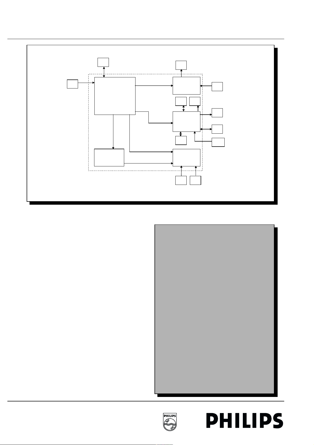
64 11. Audio video buffer FTV1.9EE Receiver Box
11.1 Functional block description
11. Audio video buffer11. 1Functional b lock description
AUDIO VIDEO BUFFER
PDP
RGB+RC5+UART
SSP
YC
SSP
HD/VD
Sounden.
POR
I†C
RC5
RGB
CONTROL
RC5
HD/
VD
Sand
castle
The function of this panel is to interface the signals between the
panels inside the Receiver box, and to interface the
Receiver- with the Display box via a VGA cable.
The audio-video buffer can be divided in 5 blocks:
– Control/RC5.
– RGB selection.
– Sandcastle generator.
– Audio selection.
– YUV to YC decoder.
The AV-buffer has several internal and external connections:
Intern:
• AUDIO, VIDEO, RC5 via Front I/O-panel
• I2C, YC, H, V, RGB, AUDIO, RC5, SOUND_ENABLE, POR
via SSP
• AUDIO via Euro-I/O
• YUV, AUDIO via YUV-panel
Extern:
• RGB_OUT, RC5, UART via sub_D (upper rear connector)
to Display Box
• AUDIO_OUT via CINCH to Display Box
• VGA_IN via sub_D (lower rear connector)
• VGA_AUDIO_IN via CINCH
• SURROUND_SOUND_CENTER_IN via CINCH-
connection (middle rear connector)
System bits
Sound-enable + por
Select
SC_2FH
YUV/ YC
i
n
L/R
Personal notes
Head-
Front
phone
L/R
AUDIO
I/O
RGB
select
RGB
H&V
VGA
EXT
YUV
L/R
L/R
L/R
RGB
RGB
SSP
CL 96532069_101.eps
I/O
PDP
SSP
Center
in
200899
Page 65
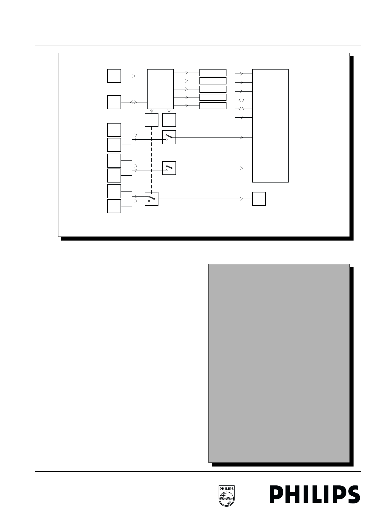
FTV1.9EE Receiver Box 11. Audio video buffer 65
11.2 Control/RC5 (See diagram AVB1)
11.2 Co ntrol/RC5 (See diagram AVB1)
CONTROL / RC5
SCL
SDA
HS
VGA
HD
SSP
7400 AVB201
I/O
EXPANDER
MONITOR
SELECT
PRESENT
7700-B
NTSC
PAL/NTSC
PAL-BG
PAL-N
PAL-M
R out
G out
B out
UART in
UART out
RC5
HS out
DISPLAY BOX
(monitor)
VS
VGA
VD
SSP
RC5
BOX
RC5
PDP
7700-A
7700-C
The I/O-expander 7400 (PCF8574) sets the system-lines that
are used in the YUV to YC decoder.
There are also the 'SELECT' and 'MONITOR PRESENT'
signals. Explanation:
• 'SELECT': This signal is fed to switch 7700A
and 7700B, to make a choice between the different
synchronisation pulses.
• 'MONITOR PRESENT': Detects whether a monitor is
present. This signal goes to switch 7700C, which is
switching the RC5 from the Receiver-box or the RC5
coming from the monitor. When the monitor is present the
RC5-receiver is only active on the monitor.
On the connector AVB201 (sub_D out) we have two UARTdatalines, which are fed to the monitor.
The UART is needed for the communication between the µP of
the E-box and the µP of the monitor.
VS out
AVB01
RC5
SSP
CL 96532069_110.eps
Personal notes
270799
Page 66
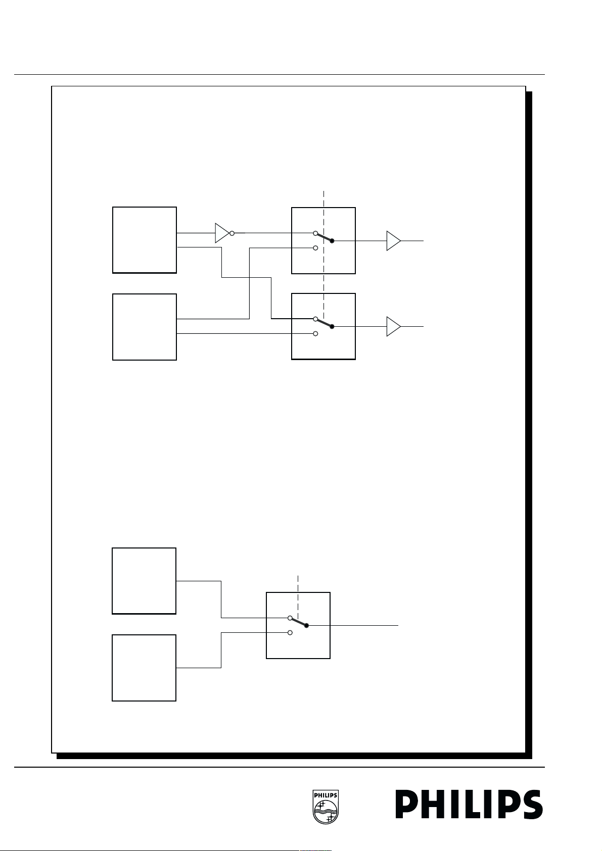
66 11. Audio video buffer FTV1.9EE Receiver Box
VIDEO SELECT
Select
7700
H
SYNC
from
SSP
7706
7706
HS_OUT
7700
SYNC
ext VGA
RGB
from
SSP
V
2, 5, 12
7706
VS_OUT
RGB SELECT
Select
7800
RGB
ext VGA
1, 3, 13
74HC4053
RGB_OUT
CL 96532069_102.eps
011099
Page 67
FTV1.9EE Receiver Box 11. Audio video buffer 67
11.3 Source selection
11.3 S ource selection
SYNC (see AVB1):
With the same SELECT signal, the matching SYNC signals are
selected.
The 2fh H-sync, coming from the SSP, is inverted in the AV
Buffer, this to ensure proper video mode recognition in
loopthrough at the 2nd display. From the R-box to the first
Monitor, video mode recognition is done via the UART bus. If a
2nd Monitor is connected via the loopthrough, the UART bus is
not longer used. So to ensure mode recognition in this case, the
H-sync is manipulated (inverted). This will be recognized by the
P in the 2nd monitor, so the correct video mode will be chosen.
µ
VIDEO (see AVB2):
The selection between RGB from the SSP (AVB59) or EXT
VGA (via sub_D) is made in the block 'RGB Select'.
The RGB-signals from the video-control-IC of the SSP go via an
emitter-follower to the switch IC7800.
The VGA signal coming from extern is divided by two and goes
via an emitter-follower to this switch IC.
The SELECT signal, coming from the I/O expander (PCF8574)
defines the position of this switch-IC (4053).
Because the output-impedance is 75 Ohm, the RGB-output
signals are amplified by two.
Personal notes
Page 68
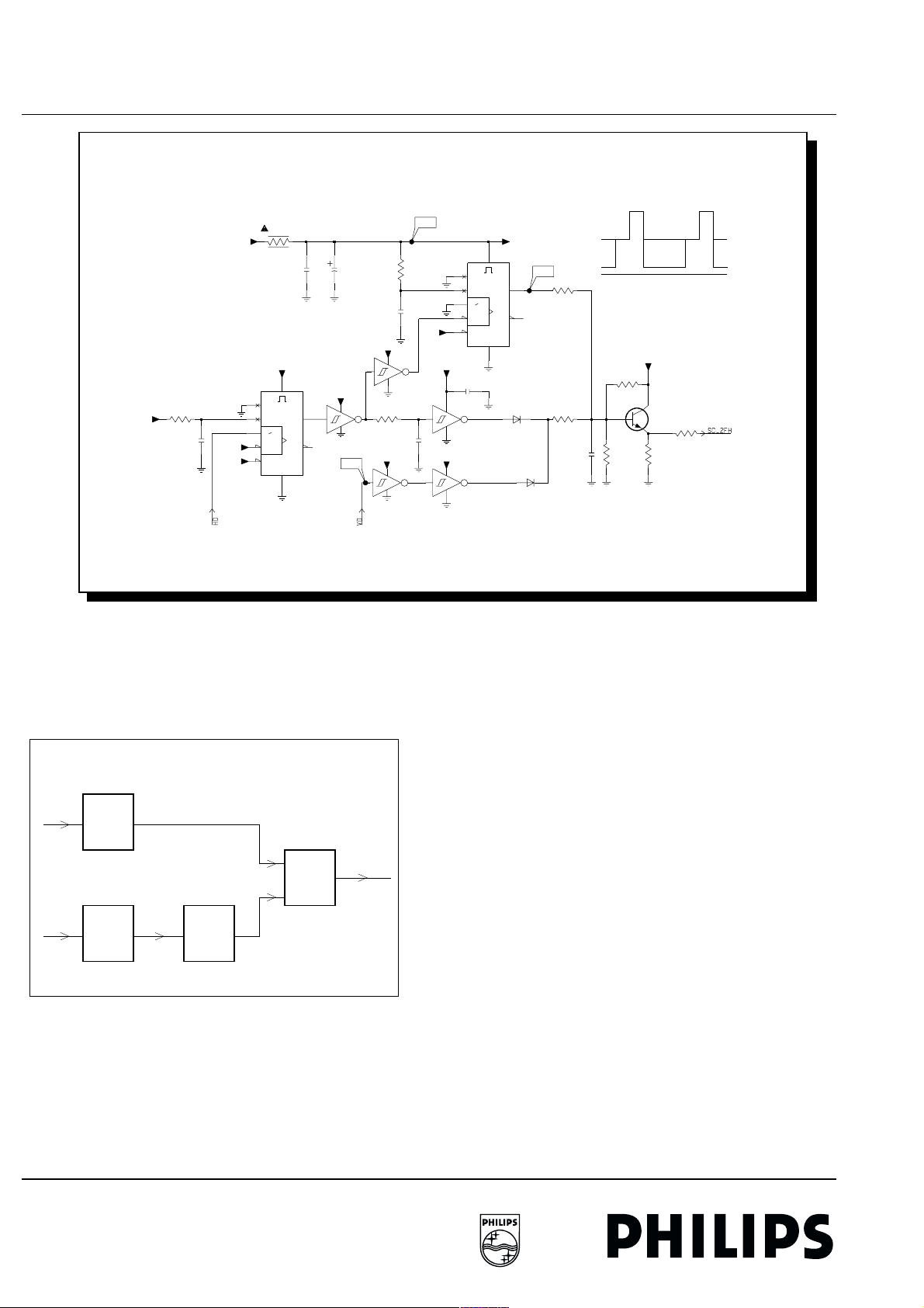
68 11. Audio video buffer FTV1.9EE Receiver Box
11.4 Sand castle generator
11.4 San d castle generator
SAND CASTLE GENERATOR
+5VA
3709
2K2
390p
2709
+5VA
+5VA
+5V2
7708-B
74HCT4538
15
CX
RCX
12
11
13
4R7
3717
+5VA
3711
2K2
3710
4.5V
2.5V
0.5V
+13V
3712
22K
7715
47K
BC847B
3715
1K
1K
3714
CL 96532069_105.eps
260799
1K
27114p7
3713
B65
CX
RCX
+5VA
16
B66
6707
BAS216
6708
BAS216
7708-A
74HCT4538
22n
2717
16
10u
2715
+5VA
14
1014
B64
3707
4K7
3708
560p
2708
+5VA
+5VA
14
+5VA
22n
7707-E
74HCT14D
1K
2707
+5VA
14
2719
14
11 10
100p
+5VA
14
13 12
SAND CASTLE GENERATOR
7707
VD
BUFFER
HD
CLAMPING BUFFER
+
SC_2FH
CL 96532069_104.eps
041099
The Video Control IC on the SSP needs a 3-level sandcastle
pulse, which is synchronised with the sync pulses of the
selected source. This sandcastle pulse is generated by two
monostable multivibrators, which are derived from the HD- and
VD-signals.
On pin 12 (7708B) we have the HD pulse that drives the first
mono stable multivibrator. R3709 and C2709 determine the
RC-time. So on pin 10 we get a pulse of 0.7 µsec. This pulse
goes via a buffer to the second mono stable multivibrator (pin 5
of 7708A), where the clamping pulse is generated.
The second mono stable multivibrator has a RC-time of 2.3
sec. Via R3711 and R3710 those two pulses are added and
µ
after the emmiter-follower we get the sandcastle-pulse.
Page 69
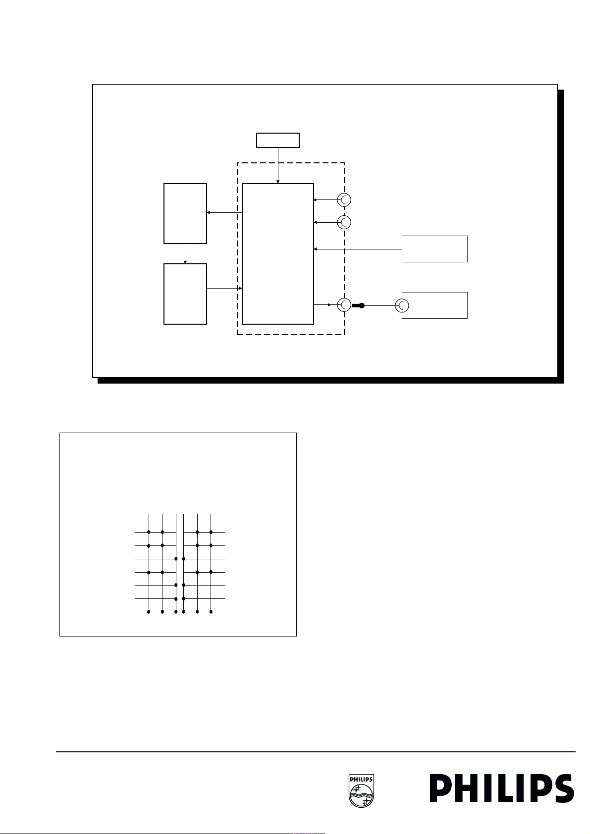
FTV1.9EE Receiver Box 11. Audio video buffer 69
11.5 Audio
11.5 A udio
SET-UP for AUDIO
FRONT I/O
L_SAT
L_FRNT
L_PRC_IN
L_YUV_IN
AUDIO_VGA_L_IN
SURROUND_SOUND_CENTER
EURO
SSP
Audio
Procsessing
L/R FRONT out
L/R SAT out
I/0
L/R_AUDIO
L/R_PRC
=processed
SET-UP for AUDIO
AUDIO_TO_MONITOR_L
L_SAT_OUT
AUDIO_TO_MONITOR_R
R_SAT_OUT
R_FRNT_OUT
L_FRNT_OUT
7901
TEA6422
10, 11
6,19
R_SAT
R_FRNT
R_PRC_IN
R_YUV_IN
AUDIO_VGA_R_IN
SURROUND_SOUND_CENTER
MUTEMUTE
L/R_AUDIO_FRONT
A/V buffer
A/V buffer
CL 96532069_109.eps
270799
8, 17
9,16
7, 18
L/R VGA in
(rear)
SURROUND center in
(rear)
YUV-panel
L/R YUV in
(rear)
DISPLAY box (monitor)
12,13
L/R AUDIO
to PDP
CL 96532069_108.eps
110899
Compared to the GFL SSP 3 inputs and 1 output: are added:
• VGA Audio input.
• YUV Audio input (optional).
• Surround Sound Center input (Display-box used as centre,
with external Dolby decoder).
• Audio output to Display-box.
Those added in-and outputs are fed to the SSP via the AVbuffer. The other in-and outputs are fed to the Euro-I/O-board.
The switching is done via the TEA6422, which is I2C-controlled.
The outputs that are not used are (software) muted to avoid
cross talk. The SOUND ENABLE and the POR-signal avoid
plops when switching on/off the set.
Page 70
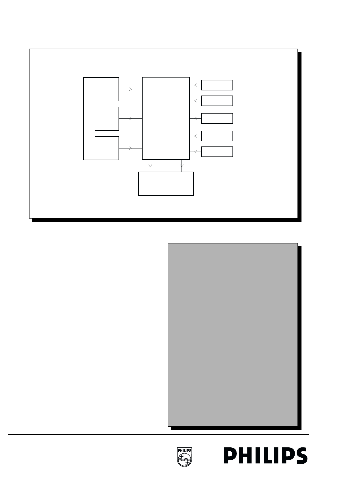
70 11. Audio video buffer FTV1.9EE Receiver Box
11.6 YUV to YC Decoder
11.6 YUV t o YC Decoder
YUV to Y/C DECODER
7130
TDA8501
Y
Y
U
V
U
1
5
1
V
The YUV to YC decoder translates the YUV-signal, coming
from a DVD-player, to an YC signal. This is necessary because
the SSP-panel can not handle YUV-signals.
Advantage is that the source-signal, fed with the YUV input,
now can be processed in several manners, e.g. Double
Window, PIP,... and can be fed to the YC output.
The frequency of the burst is dependent of the broadcasted TVsystem.
Systems that are foreseen:
• PAL-M.
• PAL-N.
• PAL-BG.
• NTSC-M.
System-selection is done via software.
Via the I/O-expander the right system-information becomes
available. In this way the right crystal is connected to the
oscillator-input (pin 23) of IC7130 (TDA8501).
The YUV-signal is amplified and fed to IC7130 (TDA8501). On
pin 4 and 17 we have the selection between PAL or NTSC.
With potmeter (R3134) we can adjust the position of the burst.
On pin 22 the Y-signal comes out and after passing a delaycircuit it is inserted back in the IC at pin 20.
The output (YC) is fed to SSP (S61) via an emitter-follower and
an impedance matching of 75 Ohm.
D
E
C
O
D
E
R
S
Y C
S
P
Personal notes
M
S
PAL M
Y
S
T
PAL N
E
PAL BG
B
I
PAL/NTSC
T
S
NTSC
CL 96532069_106.eps
260799
Page 71
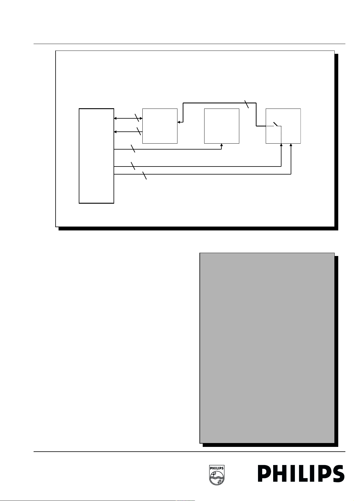
FTV1.9EE Receiver Box 12. Front I/O panel 71
12. Front I/O panel
START-UP CIRCUIT
AV41
AV44
AV15
AV155
AV33
9 fold
Control
Headphone
3 fold
3 fold
2 fold
SSP LED
S41
S44
9 fold
S01
I/O Front
Panel
The module contains external connectors for audio and video
input and push buttons to control the set. Also a two-way infra
red interaction is implemented: a receiver for a remote control
unit and a transmitter for service purposes.
A similar panel was also present in the FTV 1.5 but this one
differs from it on the following points:
• The VGA connector is no longer present.
• An extra connector is placed (AV55) to reduce the number
of wires passing from the I/O Front panel to the A/V Buffer.
Because on the A/V Buffer one line (RC5 signal) is needed,
it is not necessary to pass the panel with all 9 signal lines of
connector AV41.
• The intention was to have this new version compatible with
the FTV1.5, but changes on board outlines made this
impossible.
Figure 1 shows the interconnections between the I/O Front
Panel and direct connected PCBs. Connector types, data
directions and numbers of wires are indicated as well.
The features of the I/O Front Panel are:
• Front A/V interface (SVHS, CVBS, audio CINCH,
headphone)
• Local Controls (push buttons)
• IR receiver
• IR transmitter
LED current
RC5 SET
2 fold
Panel
Box
LP15
Received IR signals
Audio / Video
Personal notes
A / V
Buffer
AVB 01
AVB155 AVB33A
CL 96532069_154.eps
250899
Page 72
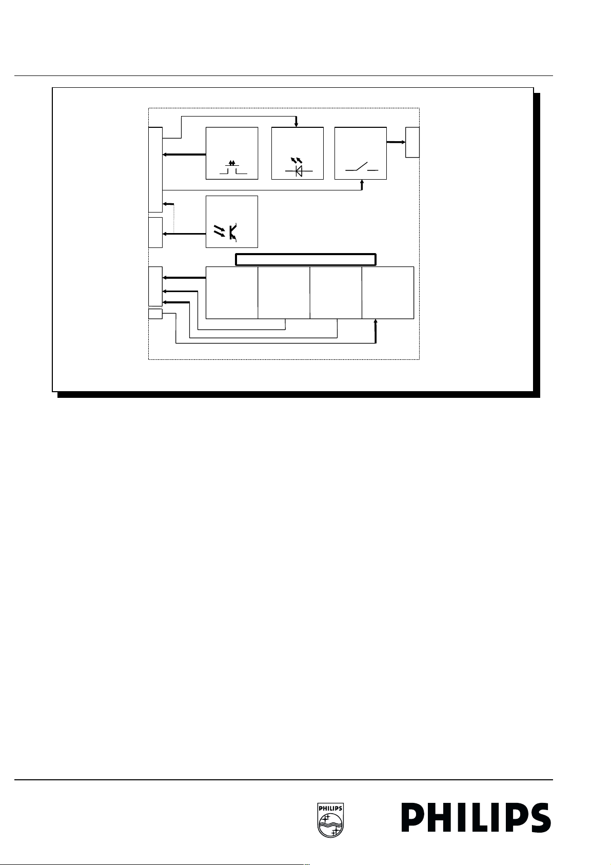
72 12. Front I/O panel FTV1.9EE Receiver Box
H
12.1 Functional diagram
12.1 Funct ional diagram
AV41 (S)
9 fold
JST B9B-EDM-BK
(opt. 1.5)
2 fold
JST B2B-EH-A
AV155 (AVB)
AV33 (AVB)
JST B9B-EDM-WH
9 fold
3 fold
AV44 (S)
JST B03B-EDM-WH
Push
Buttons
IR
receiver
SVHS
connector
IR
transmitter
Front A / V Interface
CVBS
connector
LED
switches
AUDIO
connectors
Front I/O Panel E-Box
CL 96532069_165.eps
JST B03B-EDM_W
3 fold
AV15 (LD)
headphone
connector
020999
Front I/O Interface
The front I/O interface has the following features:
• Input for CVBS, Y/C and stereo audio signals.
• Connection for headphones.
• Termination resistors and ESD protection diodes.
• Audio cinch connectors both contain mechanical switches:
when only one audio cinch is connected the (mono) signal
will be connected to both left and right audio channels.
• Chrominance input with a high impedance for DC and with
a 75 ohm impedance for AC.
Push buttons
The local keyboard contains 5 buttons:
• Volume up ( V+ )
• Volume down ( V- )
• Page Up ( P+ )
• Page down ( P- )
• Installation ( Inst )
Pressing one of these buttons connects 2 signal lines together,
coming from the microprocessor on the SSP panel.
Infra Red Receiver
The infra red receiver output is connected to connector
(AV155), to give the possibility to select the display IR receiver
or the E-Box IR receiver. This selection will be done in the A/V
Buffer.
Infra Red Transmitter
The IR transmitter diode is configured in an emitter follower with
a PNP transistor. This makes it possible to achieve large
currents through the IR LED what will enhance the emitting
range. The IR transmitter is used for service purposes.
LED indication
A two-colour LED is located on the 'LED Panel Box'. The I/O
Front Panel creates a limited current to supply the LED. This
LED is a bi-colour type which are actually two LED's in one
housing.
Page 73
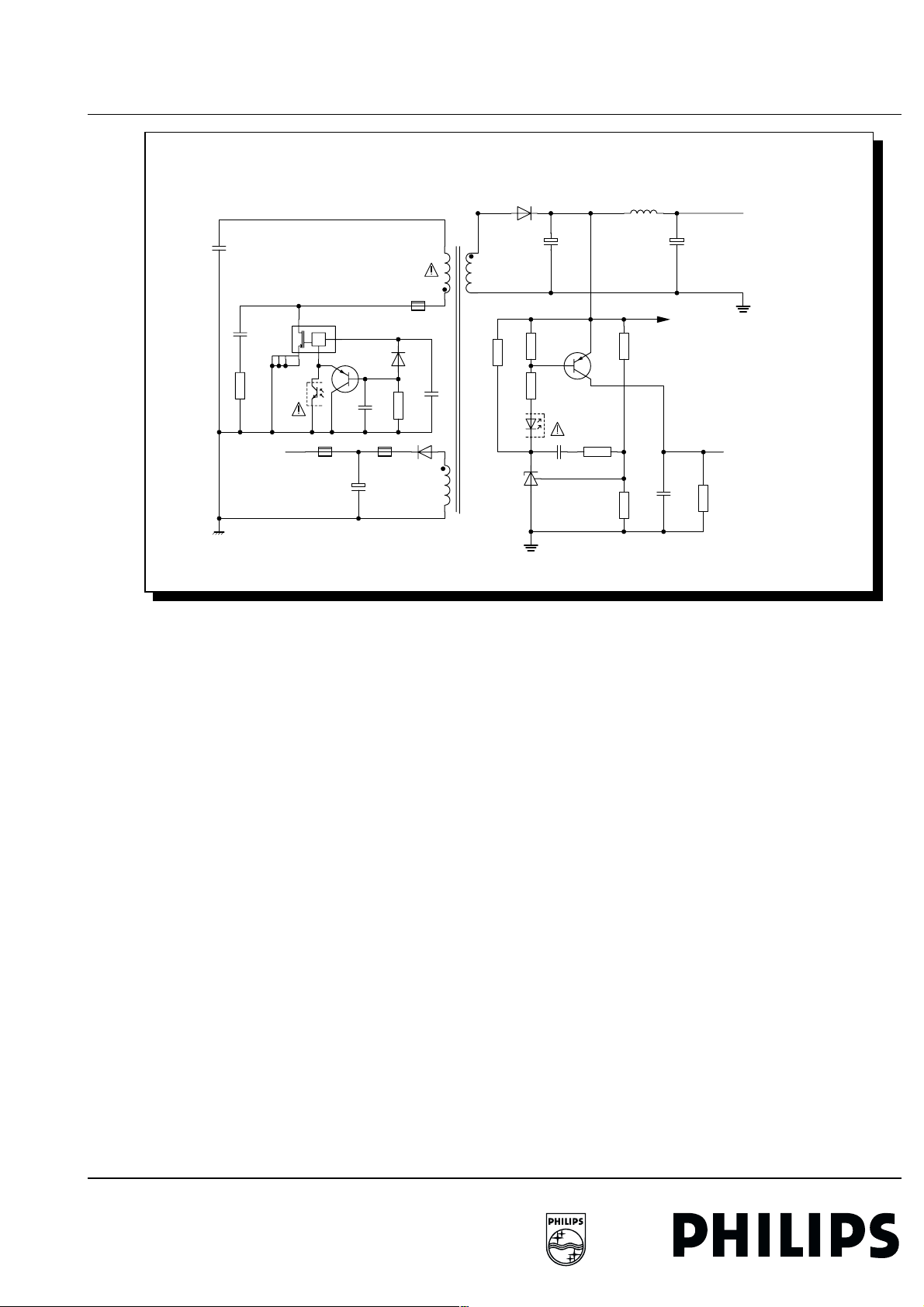
FTV1.9EE Receiver Box 13. Power supply 73
13.1 Standby supply
13. Power supply13.1Standb y supply
START-UP CIRCUIT
e
c
R71
10K
T6
BC557B
L6
10UH
R68
2K61
R72
2K43
+5VstbyU
C63
100N
50V
C54
390U
10V
R73
3K3
+5Vstdby
C60
470P
400V
C51
47P
630V
220E
+12Vprim
D
S
6
32
CNY17-F3
OC3-B
5
87
IC4
TNY253P
EN
4
5
4
L7
BP
1
BC557B
e
c
D25
SB160
C53
R69
2K2
1
R66R60
1K
CNY17-F3
1
2
k
r
a
390U
10V
b
OC3-A
C55
100N 50V
TR2
1
C62
50V
100N
-
8
7
2
R67
1K
3
4
-
IC3
TL431CLP
7663692
L12
4S2
T5
b
1
2
C50
10U
50V
C64
100N
50V
L10
D30
1N4148
R84
1M2
D22
MBR1100
General
To enable an energy-efficient stand-by power supply, to less
than 100 mW, a controller chip called TinySwitch of Power
Integrations Inc. is used.
The TinySwitch, TNY253 rated for 5 W supplies, requires very
few external components.
The output power is proportional to the primary inductance of
the transformer, and is independent of the input voltage.
Designed to be a simple, on/off control device, the TinySwitch
is integrated on chip: 700 V power MOSFET; oscillator; highvoltage, switched-current source; current limit; and thermal
shutdown circuitry.
The maximum on-time of the power MOSFET is determined by
the duty cycle signal (Dmax) of the internal oscillator. Also, the
current limit and switching frequency (44 kHz) for the TNY253
are fixed, while the power delivered is proportional to the
primary inductance of the transformer.
The TinySwitch is powered directly by the incoming high
voltage, it eliminates the need for an auxiliary bias winding and
associated circuitry, thereby simplifying the design of the
transformer.
The thermal shutdown threshold is set at 135°C. When the
junction temperature exceeds 135°C, the power MOSFET is
disabled until the die-junction temperature goes under 70°C.
The TNY253 switches at 44 kHz to minimise EMI filtering
requirements, and permits the use of a simple snubber clamp
to limit drain spike voltage.
CL 96532069_049.eps
140799
Start-up circuit
Switching on the set, C60 is charged via the diode-bridge D1D4 to a DC-voltage between 150 and 300V, depending on the
input voltage. IC4 is supplied directly by the incoming high
voltage. When the on-chip oscillator is enabled, it turns the
power MOSFET on at the start of each cycle. The MOSFET is
turned-off as soon as the output current reaches the upper limit.
Control circuit and oscillation phase
Unlike a conventional PWM controller, it uses an on/off control
to regulate the output voltage. IC3 (TL431) and OC3 (OptoCoupler) form the secondary voltage "regulation circuit".
IC4 is enabled/disabled by the opto-coupler-transistor
connected at pin 4. If the current through the opto-couplertransistor exceeds the 50µA the Tinyswitc is disabled.
The feedback is realised as follows: When the output voltage
5Vstdby increases (decrease of the load), the voltage at
resistor R72 increases. As a result, the internal resistance of
IC3 decreases and results in a current through the diode in the
opto-coupler OC3. At the same time a current flows through
through the transistor part of OC3, disabling IC4. At the
beginning of each clock cycle, the Tinyswitch samples the
ENABLE pin to decide whether or not to start a switching cycle.
If the ENABLE pin is below its internal threshold voltage no
switching cycle occurs. If at the next sample the voltage at the
ENABLE pin reaches its threshold voltage, a switching cycle
occurs. If not there again is no switching cycle.
Page 74
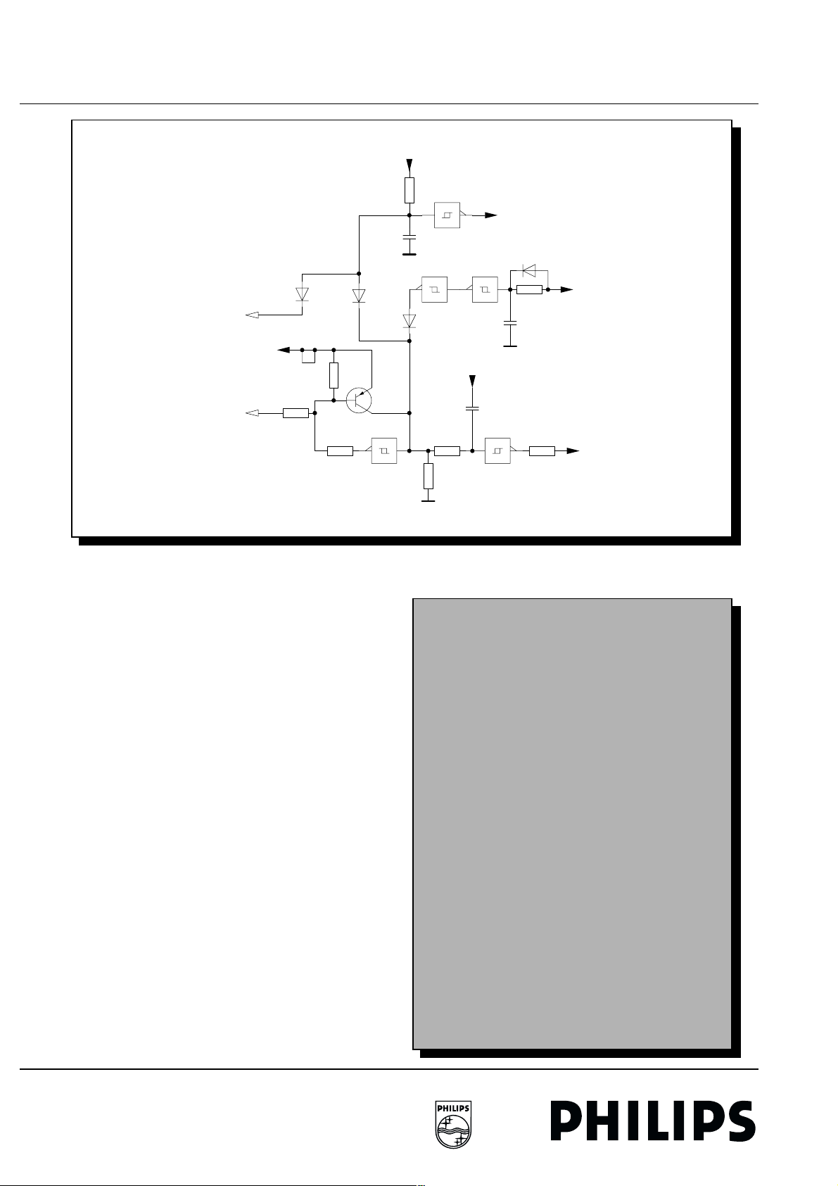
74 13. Power supply FTV1.9EE Receiver Box
13.2 Switch ON behaviour
13.2 Swit ch ON behaviour
POR CIRCUIT
+5Vstdby
R74
1M8
IC5-F
74HC14
MAINSDIP
FB1
5.1VU
R76
22K
jumper
J4
D26
1N4148
1M
R77
R75
47K
13
C56
100N
50V
GND
74HC14
4
D27
1N4148
D28
1N4148
T7
e
b
BC557B
c
IC5-C
74HC14
5
6
IC5-B
R81
1M
R78
1K
12
74HC14
3
2
+5Vstdby
IC5-A
9
C59
100N
50V
IC5-D
74HC14
POR
1
GND
D29
BAT85
2 1
2M7
R79
C57
22N
50V
R82
47K
8
STBY
SC
The start-up and shut down is very much different from the GFL
behaviour, due to the different power supply architecture.
The POR circuit is shown above.
The POR pulse is used to initialise the microprocessor and
other IC's.
After switching on the set via the mains switch, the +5Vstdby is
available after approx. 200 msec.
The POR pulse becomes high immediately because C56 is
discharged at the moment of switching on.
After a certain time C56 has charged up and reaches the input
voltage at which the output of the inverter changes polarity from
"1" to "0".
The total start-up time is approx. 700 msec.
After the reset of the µP, the µP decides, based upon the stored
information, whether the set should remain in standby or should
be switched on.
In case the set should switch on, the standby signal goes
logically low. This logic low level of the standby signal triggers
the inverter Schmitt-trigger - IC5A and IC5B. The output of IC5B
changes from a logic "1' to "0". Due to this transition signal SC
(base of transistor T2) connected via resistor to output IC5-D
changes from a logic "1" to "0". During this logic "1", transistor
T2 was conducting, connecting the base of transistor T3 to
ground, disabling the current through opto-coupler OC1 and the
+12Vprim is not connected to pin 7 of IC1 - UC3842.
GND
CL 96532069_050.eps
Personal notes
041099
Page 75
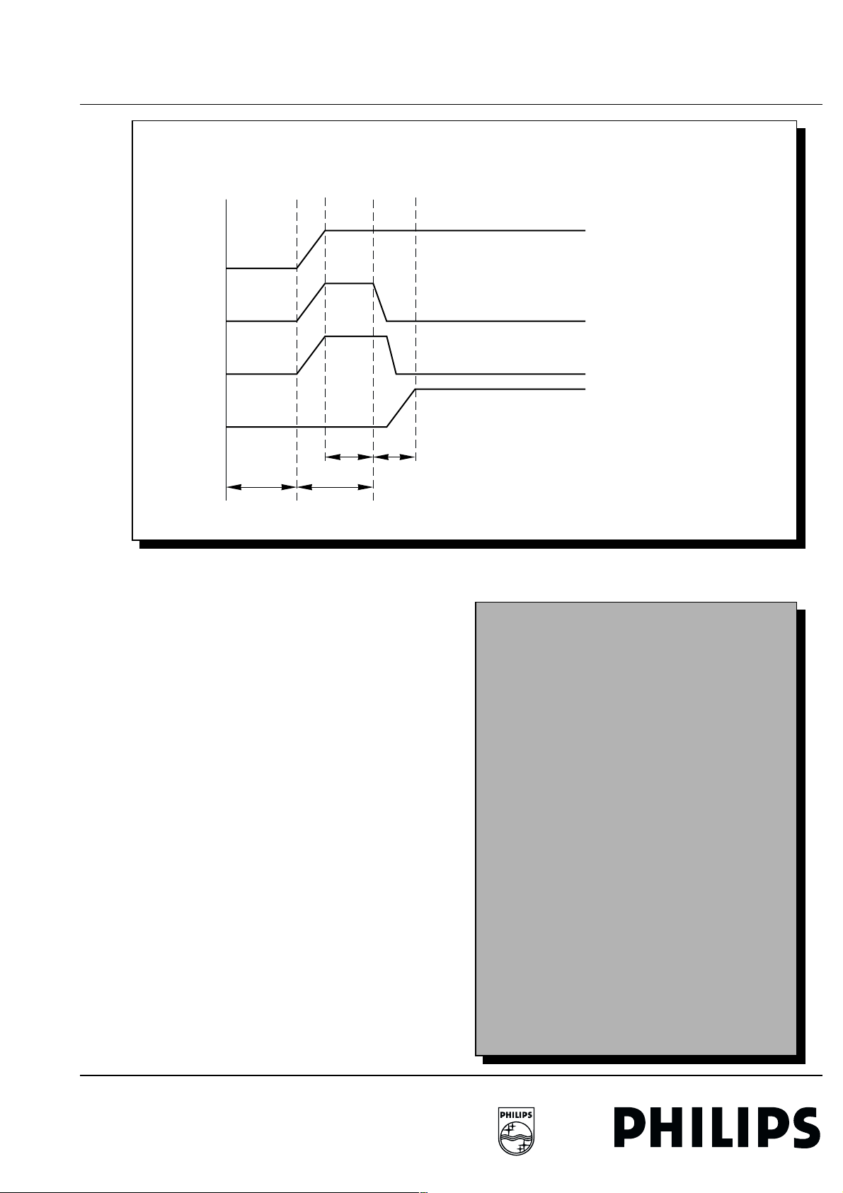
FTV1.9EE Receiver Box 13. Power supply 75
13.2 Switch ON behaviour
SWITCH ON
+5VSTBY
POR
STANDBY
OTHER SUPPLY
VOLTAGES
>0.1s <0.5s
200ms 150ms
t=0
Other situations where a POR pulse is generated:
Mains dip.
The +5Vstby will drop in voltage. Transistor T6 stops
conducting, which results in a voltage drop across resistor R72
and capacitor C63. Due to this voltage drop, C56 is discharged
and goes below the low input of the Schmitt-trigger. The output
of IC5-F generates a POR pulse.
Heavy Load or short-circuit of the +5V2, 8V6, 13V and/or
40V.
When the output is too much loaded or short-circuited, the
regulation circuit consisting of IC2, several resistors and
capacitor and opto-coupler OC2 gets out of regulation, and
signal-point Fb1 rises. If the voltage rises too much, transistor
T7 stops conducting and the voltage across resistor R78 will
drop. As a result C56 is discharged and goes below the low
input of the Schmitt-trigger. The output of IC5-F generates a
POR pulse. The set is switched to standby.
The other that will happen is that the output of IC5_D changes
from "0" to "1". Transistor T2 starts conducting and connects
the base of T3 to ground. The current through the diode of OC3
stops and IC1 is no longer supplied via the +12Vprim. The
supply stops.
Personal notes
CL 96532069_051.eps
150799
Page 76
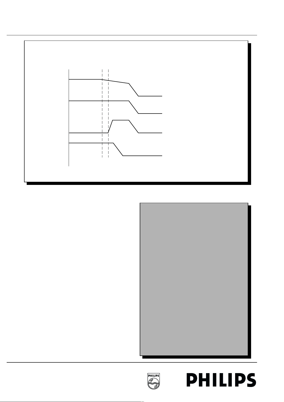
76 13. Power supply FTV1.9EE Receiver Box
13.3 Switch OFF behaviour
13.3 Swit ch OFF behaviour
SWITCH OFF
VI
+5VSTBY
POR
OTHER SUPPLY
t=0
VOLTAGES
When the mains switch ( 1004 ) is pressed to switch OFF the
E-box, the voltage at the mains elco starts decreasing. At a
certain moment, it reaches a level that is regarded as a mainsdip, see mains-dip at the previous paragraph. A POR pulse is
generated before the +5Vstby and the other supply voltages
start decreasing.
This POR pulse is generated to avoid the main µP from wrong
protections and/or error-codes.
CL 96532069_052.eps
Personal notes
150799
Page 77
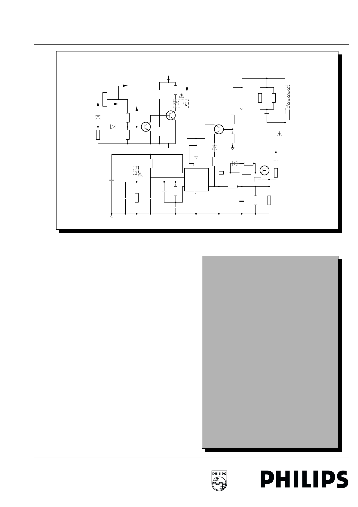
FTV1.9EE Receiver Box 13. Power supply 77
13.4 Main supply
13.4 Ma in supply
MAIN SUPPLY
+5.1V
SU02
D14
4V7
R26
220E
K5
K-3P
3
2
1
D15
1N4148
C10
100N
50V
POR
STBY
R25
47K
R39
22K
1N
50V
4
SC
5
T2
BC547B
b
OC2-B
R6
1K
c
e
CNY17-F3
R5
4K7
C12C11
10N
50V
+5VstbyU
R27
4K7
T3
BC547B
b
R28
1K
C13
22N
50V
+12Vprim
R29
100E
1
5
OC1
CNY17-F3
2
4
c
e
7
Vcc
8
V_ref
4
Rt/Ct
2
V_fb
1
Comp
R7
GND
10K
C14
10N
50V
jumper
5
J12
C9
100N
50V
UC3843
IC1
Output
Current
sense
6
3
T4
BC547B
c
e
D5
6V8
R41
2K2
b
4S2
L11
C15
4N7
50V
R10
220E
D10
BAT85
R40
3M3
R42
150K
R9
220E
C5
470P
400V
R8
150E
C16
100N
50V
2SK2333
KB8
1
Plated
1E2
-
2
R22
220E
T1
g
S1
R14
220E
4
C4
680P
630V
TR1
7662661
C17
100P
630V
d
R13
s
470E
R12R11
1E2
General Information
The E-box power supply is a Switch Mode Power Supply
(SMPS) with a current regulating pulse width modulator IC1UC3843. The topology is a flyback converter with primary
current sensing, secondary voltage sensing and mains input
measuring.
The SMPS works in discontinuous mode, so with a T-on, T-off
and a T-dead.
Depending on the measured voltage and current the switching
MOSFET is driven for a longer or shorter period
Output voltages
• 5V_stb (SSP µP & Control, Euro I/O, AV Buffer, LED panel
and front I/O) : + 5V1 This voltage is also present during
standby.
• 5V2 (SSP, FBX 4, Euro NICAM, AV Buffer, DW and TXT
panel) : + 5V3
• 8V6 (SSP, and Euro I/O panel) : 8V8
• +12V8 (SSP, Incredible Stereo (AY), FBX 4, Euro NICAM,
AVB and DW) : 12V6
• +33V (SSP-front-end, DW) : 40V
Personal notes
CL 96532069_053.eps
040899
The circuit
The regulator IC7203 UC3842
Page 78
78 13. Power supply FTV1.9EE Receiver Box
13.4 Main supply
The +12 Vprim is via opto-coupler OC1 connected to pin 7; this
voltage must exceed 8V5 to start-up the IC (this may not drop
below 7 V during operation).
The oscillator
The IC contains an internal oscillator whose frequency and duty
cycle is set by resistor R5 and a capacitor C12, connected to
pin 8 and pin 4.
Stabilisation
By increasing the load on a secondary voltage, all secondary
voltages will drop, resulting in a voltage drop on V-ref of IC2 connected to resistor R36. This causes an increase of the
voltage at the cathode of IC2 and decreases the current
through the diode of opto-coupler OC2, which results in a
voltage decrease at pin 2 of IC1 - UC3843. A voltage decrease
results in a delay in the MOSFET switch-off time. More energy
is stored in the transformer while the MOSFET conducts longer,
causing an increase in the secondary voltage.
Overload/ Short circuit
During overload the secondary voltages drop rapidly, resulting
in a strong drop of the voltage at V-ref of IC2 - connected to
resistor R36. As a result signal-point Fb1 rises fast and
transistor T7 of the POR-circuit stops conducting. As a result
C56 is discharged and goes below the low input of the Schmitttrigger. The output of IC5-D changes from "0" to "1". Transistor
T2 is switched on and connects the base of T3 to ground. The
current through the diode of OC3 stops and IC1 is no longer
supplied via the +12Vprim.
The supply stops and the set is switched to Standby.
The circuit
• The mains voltage is rectified by bridge rectifier D1, D2, D3
and D4 and filtered by C6. The DC voltage across C6 is the
DC input voltage for the SMPS at pin 2 of transformer TR1.
• R5 and C12 set the external oscillator frequency; the
frequency is approximately 35 kHz.
• Stabilisation occurs via the +12.8V and the +5V2 output
voltages which are both fed back to pin 2 of the control IC
via the secondary regulation circuit consisting of IC2 and
opto-coupler OC-2.
• Current measurement is performed by R11//R12, which
voltage is fed back to pin 3.
• Mains voltage control via R40 and R42. R42 couples a part
of the rectified mains voltage to pin 3 of IC1. Due to a higher
mains input voltage, the voltage at the base of T4 will
increase, resulting in a higher DC-voltage at the emitter of
T4. The voltage at pin 3 of IC1 is formed by the dividing of
R10 and R41 of the voltage at the emitter of T4 minus a
zener voltage of 6V8.
Switching the set to standby.
The signal STBY goes from a logic "0" to "1". Transistor T2 is
switched on via R25 and the base of T3 is grounded. The
current flow through the diode of opto-coupler OC1 stops and
IC1 is disconnected from the +12Vprim.
The power supply stops operating.
Personal notes
Page 79
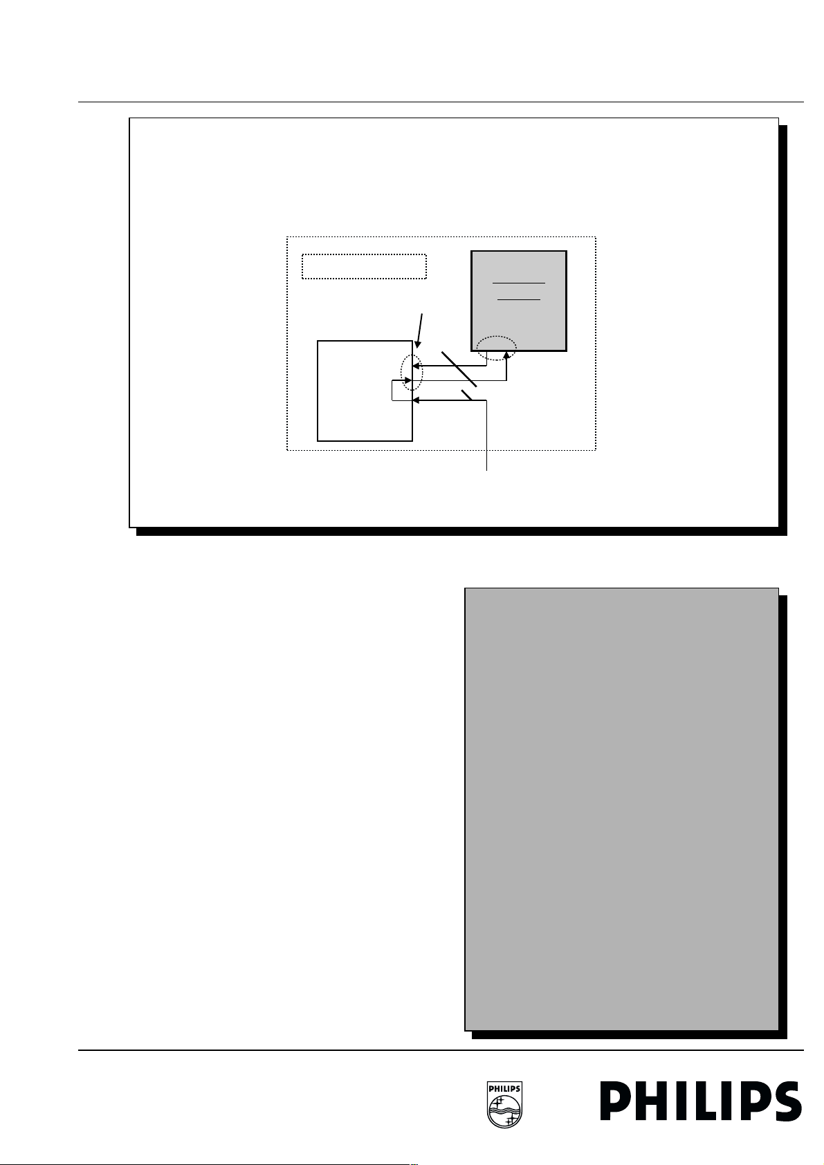
FTV1.9EE Receiver Box 14. Switch panel 79
14. Switch panel
START-UP CIRCUIT
E-BOX
(partial)
JST B7P-VH
SU161
SUPPLY
SU162
This module contains a mains switch to turn the E-Box power
"ON" or "OFF" and a connector to connect the panel to the
Supply Panel.
The mains switch enables the user to turn the E-box "ON" and
"OFF" by interrupting the mains line to the electronics.
Figure above shows two modules of the E-Box: the Switch
Panel, Supply and mutual connections.
The Mains Switch interrupts the power lines 'F-phase' and 'Fneutral'. The output of the switch consists of the lines 'S-phase'
and 'S-neutral'.
Mains
JST
B3P-VH
out
SWITCH
PANEL
SE161
4 fold
2 fold
JST B7P-VH
Mains in
Mains input
CL 96532069_156.eps
Personal notes
250899
Page 80
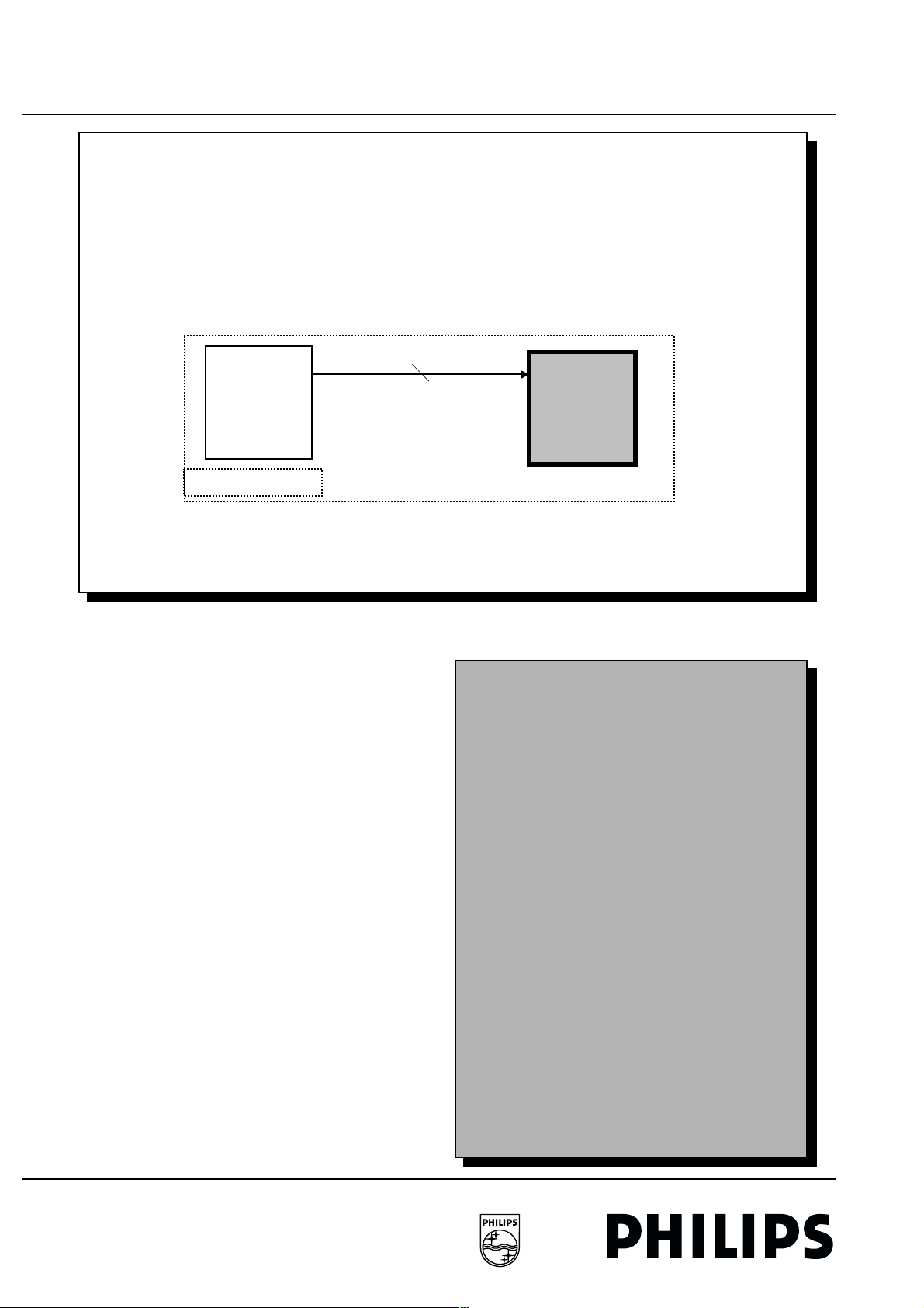
80 15. LED panel FTV1.9EE Receiver Box
15. LED panel15.1LED Mod ule
START-UP CIRCUIT
AV15
FRONT I/O
E-BOX
(partial)
JST B03B-EDM-WH
This module contains a single bi-colour LED to indicate the
state of the E-Box. The colours of de LED are red, green and
orange (if both red and green are on).
The states are shown as follows:
• Red : Standby mode
• Green : Normal operating mode
• Orange : Semi-standby mode
The Front I/O panel supplies the LED by a limited current.
Figure above shows three modules of the E-Box: the LED
Panel, Front I/O, Supply and mutual connections.
3 fold
JST B03B-EDM-WH
Personal notes
LE15
LED PANEL
CL 96532069_157.eps
250899
Infra Red Receiver
The infra red receiver output is connected to connector
(AV155), to give the possibility to select the Display Box- or the
Receiver Box IR receiver. This selection will be done in the A/V
Buffer.
Infra Red Transmitter
The IR transmitter diode is configured in an emitter follower with
a PNP transistor. This makes it possible to achieve large
currents through the IR LED what will enhance the emitting
range. The IR transmitter is used for service purposes.
 Loading...