

Page 1

查询TJA1054A供应商
INTEGRATED CIRCUITS
DATA SH EET
TJA1054A
Fault-tolerant CAN transceiver
Product specification
Supersedes data of 2002 Feb 11
2004 Mar 23
Page 2

Philips Semiconductors Product specification
Fault-tolerant CAN transceiver TJA1054A
FEATURES
Optimized for in-car low-speed communication
• Baud rate up to 125 kBaud
• Up to 32 nodes can be connected
• Supports unshielded bus wires
• Very low ElectroMagnetic Emission (EME) due to
built-in slope controlfunction and a very good matching
of the CANL and CANH bus outputs
• Good ElectroMagnetic Immunity (EMI) in normal
operating mode and in low power modes
• Fully integrated receiver filters
• Transmit Data (TxD) dominant time-out function.
Bus failure management
• Supports single-wire transmission modes with ground
offset voltages up to 1.5 V
• Automatic switching to single-wire mode in the event of
bus failures, even when the CANH bus wire is
short-circuited to V
CC
• Automatic reset to differential mode if bus failure is
removed
• Full wake-up capability during failure modes.
Protections
• Bus pins short-circuit safe to battery and to ground
• Thermally protected
• Bus lines protected against transients in an automotive
environment
• An unpowered node does not disturb the bus lines.
GENERAL DESCRIPTION
The TJA1054A is the interface between the protocol
controller and the physical bus wires in a Controller Area
Network (CAN). It is primarily intended for low-speed
applications up to 125 kBaud in passenger cars. The
device provides differential receive and transmit capability
but will switch to single-wire transmitter and/or receiver in
error conditions.
The TJA1054A is the ESD improved version of the
TJA1054. For an overview of the differences between the
TJA1054 and the TJA1054A, please refer to “Appendix A”.
The TJA1054AT is, as the TJA1054T, pin and downwards
compatiblewiththePCA82C252TandtheTJA1053T. This
means that these two devices can be replaced by the
TJA1054AT or the TJA1054T with retention of all
functions.
Themost important improvements of the TJA1054 and the
TJA1054A with respect to the PCA82C252 and the
TJA1053 are:
• Very low EME due to a very good matching of the CANL
and CANH output signals
• Good EMI, especially in low power modes
• Full wake-up capability during bus failures
• Extended bus failure management including
short-circuit of the CANH bus line to V
CC
• Support for easy system fault diagnosis
• Two-edge sensitive wake-up input signal via pin WAKE.
Support for low power modes
• Low current sleep and standby mode with wake-up via
the bus lines
• Power-on reset flag on the output.
ORDERING INFORMATION
TYPE
NUMBER
NAME DESCRIPTION VERSION
PACKAGE
TJA1054AT SO14 plastic small outline package; 14 leads; body width 3.9 mm SOT108-1
TJA1054AU − bare die; 1990 × 2730 × 375 µm −
2004 Mar 23 2
Page 3

Philips Semiconductors Product specification
Fault-tolerant CAN transceiver TJA1054A
QUICK REFERENCE DATA
SYMBOL PARAMETER CONDITIONS MIN. TYP. MAX. UNIT
V
CC
V
BAT
I
BAT
V
CANH
V
CANL
∆V
∆V
t
PD(L)
t
r
t
f
T
vj
CANH
CANL
supply voltage on pin V
CC
4.75 − 5.25 V
battery voltage on pin BAT no time limit −0.3 − +40 V
operating mode; note 1 5.0 − 27 V
load dump −−40 V
battery current on pin BAT sleep mode; VCC=0V;
V
=12V
BAT
CANH bus line voltage VCC= 0 to 5.0 V; V
BAT
≥ 0V;
− 30 50 µA
−27 − +40 V
no time limit
CANL bus line voltage VCC= 0 to 5.0 V; V
BAT
≥ 0V;
−27 − +40 V
no time limit
CANH bus line transmitter
I
= −40 mA −−1.4 V
CANH
voltage drop
CANL bus line transmitter
I
=40mA −−1.4 V
CANL
voltage drop
propagation delay TXD (LOW)
− 1 −µs
to RXD (LOW)
bus line output rise time between 10% and 90%;
− 0.6 −µs
C1 = 10 nF; see Fig.5
bus line output fall time between 10% and 90%;
− 0.3 −µs
C1 = 1 nF; see Fig.5
virtual junction temperature −40 − +150 °C
Note
1. A local or remote wake-up event will be signalled at the transceiver pins RXD and NERR if V
(see Table 2).
=5.3Vto27V
BAT
2004 Mar 23 3
Page 4
Philips Semiconductors Product specification
Fault-tolerant CAN transceiver TJA1054A
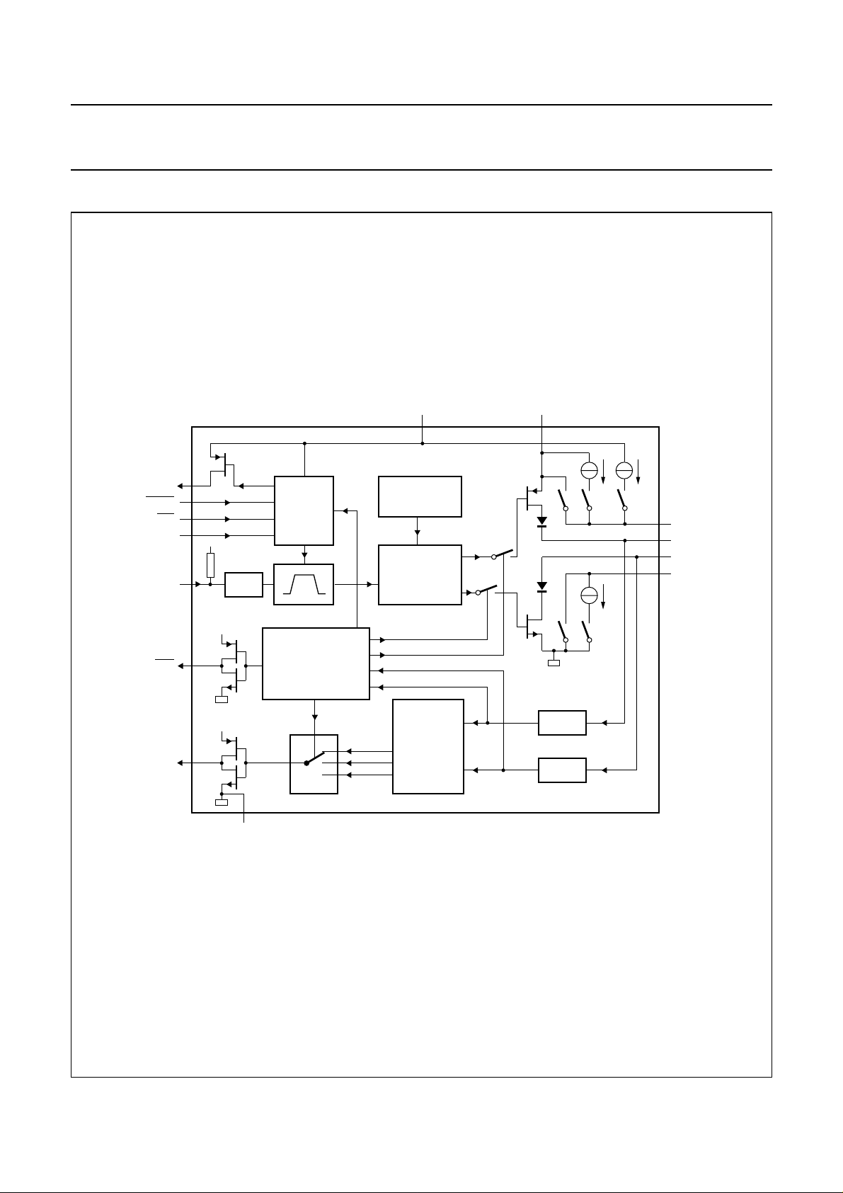
BLOCK DIAGRAM
handbook, full pagewidth
WAKE
STB
TXD
ERR
RXD
INH
EN
BAT
14
1
7
5
6
V
CC
2
TIMER
V
CC
4
V
CC
3
GND
WAKE-UP
STANDBY
CONTROL
FAILURE DETECTOR
PLUS WAKE-UP
PLUS TIME-OUT
13
TEMPERATURE
PROTECTION
DRIVER
TJA1054A
RECEIVER
V
CC
10
FILTER
FILTER
9
RTL
11
CANH
12
CANL
8
RTH
MGU383
Fig.1 Block diagram.
2004 Mar 23 4
Page 5
Philips Semiconductors Product specification
Fault-tolerant CAN transceiver TJA1054A
PINNING
SYMBOL PIN DESCRIPTION
INH 1 inhibit output for switching an external voltage regulator if a wake-up signal occurs
TXD 2 transmit data input for activating the driver to the bus lines
RXD 3 receive data output for reading out the data from the bus lines
ERR 4 error, wake-up and power-on indication output; active LOW in normaloperating mode when the bus
has a failure, and in low power modes (wake-up signal or in power-on standby)
STB 5 standby digital control signal input (active LOW); together with the input signal on pin EN this input
determines the state of the transceiver (in normal and low power modes); see Table 2 and Fig.3
EN 6 enable digital control signal input; together with the input signal on pin STB this input determines
the state of the transceiver (in normal and low power modes); see Table 2 and Fig.3
WAKE 7 local wake-up signal input (active LOW); both falling and rising edges are detected
RTH 8 termination resistor connection; in case of a CANH bus wire error the line is terminated with a
predefined impedance
RTL 9 termination resistor connection; in case of a CANL bus wire the line is terminated with a predefined
impedance
V
CC
CANH 11 HIGH-level CAN bus line
CANL 12 LOW-level CAN bus line
GND 13 ground
BAT 14 battery supply voltage
10 supply voltage
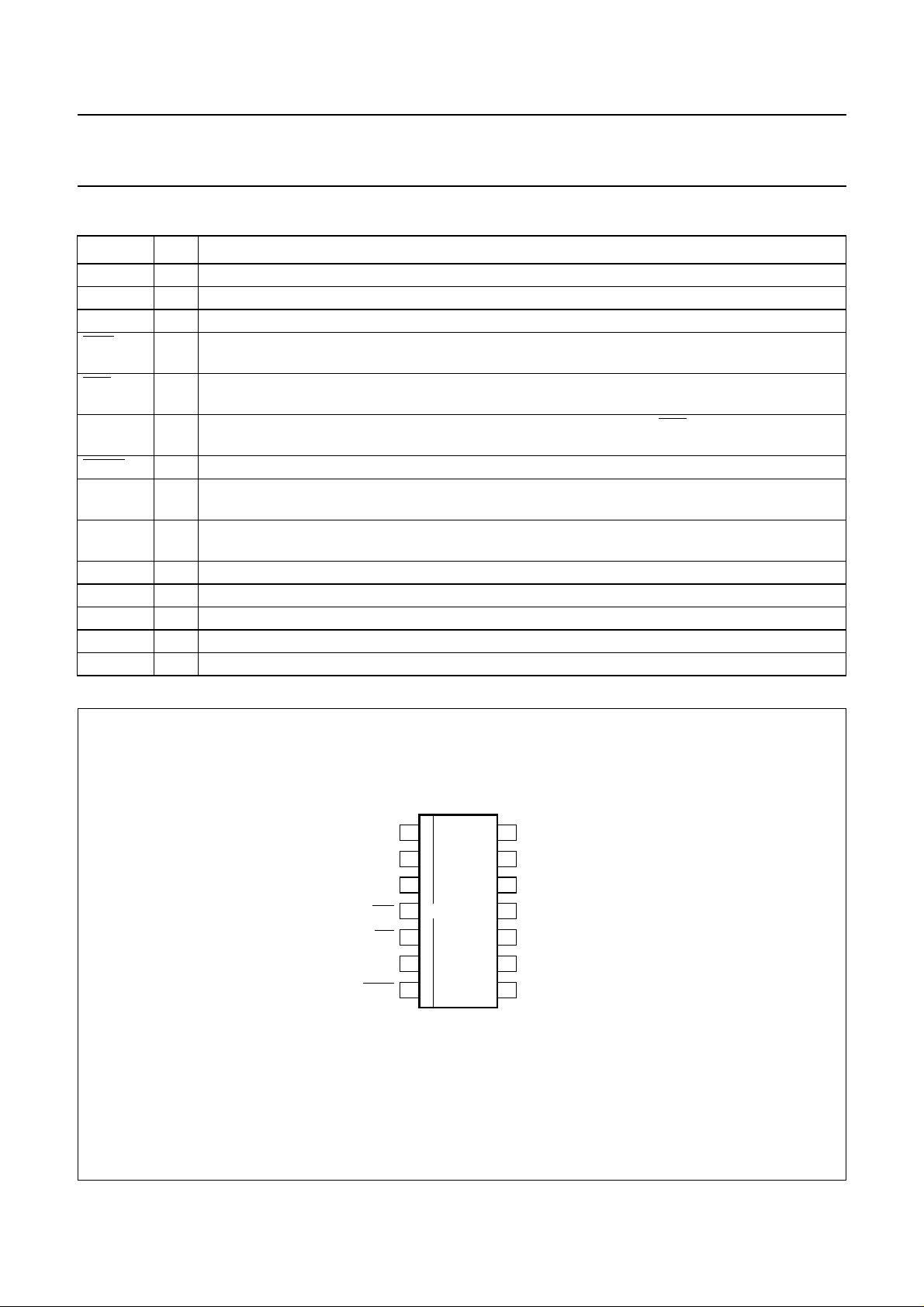
handbook, halfpage
1INH
2
TXD GND
3
RXD CANL
4
ERR CANH
STB V
WAKE RTH
TJA1054AT
5
6
EN RTL
7
Fig.2 Pin configuration.
2004 Mar 23 5
MGU379
14 BAT
13
12
11
10
CC
9
8
Page 6

Philips Semiconductors Product specification
Fault-tolerant CAN transceiver TJA1054A
FUNCTIONAL DESCRIPTION
The TJA1054A is the interface between the CAN protocol
controller and the physical wires of the CAN bus (see
Fig.7). It is primarily intended for low-speed applications,
up to 125 kBaud, in passenger cars. The device provides
differential transmit capability to the CAN bus and
differential receive capability to the CAN controller.
To reduce EME, the rise and fall slopes are limited. This
allows the use of an unshielded twisted pair or a parallel
pair of wires for the bus lines. Moreover, the device
supportstransmission capability on either bus line if one of
the wires is corrupted. The failure detection logic
automatically selects a suitable transmission mode.
In normal operating mode (no wiring failures) the
differential receiver is output on pin RXD (see Fig.1).
The differential receiver inputs are connected to
pins CANH and CANL through integrated filters.
The filtered input signals are also used for the single-wire
receivers. The receivers connected to pins CANH
and CANL have threshold voltages that ensure a
maximum noise margin in single-wire mode.
A timer function (TxD dominant time-out function) has
been integrated to prevent the bus lines from being driven
into a permanent dominant state (thus blocking the entire
network communication) due to a situation in which
pin TXD is permanently forced to a LOW level, caused by
a hardware and/or software application failure.
If the duration of the LOW level on pin TXD exceeds a
certain time, the transmitter will be disabled. The timer will
be reset by a HIGH level on pin TXD.
Failure detector
The failure detector is fully active in the normal operating
mode. After the detection of a single bus failure the
detector switches to the appropriate mode (see Table 1).
The differential receiver threshold voltage is set at −3.2 V
typical (VCC= 5 V). This ensures correct reception with a
noise margin as high as possible in the normal operating
mode and in the event of failures 1, 2, 5 and 6a. These
failures, or recovery from them, do not destroy ongoing
transmissions. The output drivers remain active, the
termination does not change and the receiver remains in
differential mode (see Table 1).
Failures 3, 3a and 6 are detected by comparators
connected to the CANH and CANL bus lines.
Failures 3 and 3a are detected in a two-step approach.
If the CANH bus line exceeds a certain voltage level, the
differential comparator signals a continuous dominant
condition. Because of inter operability reasons with the
predecessor products PCA82C252 and TJA1053, after a
first time-out the transceiver switches to single-wire
operation through CANH. If the CANH bus line is still
exceeding the CANH detection voltage for a second
time-out, the TJA1054A switches to CANL operation; the
CANH driver is switched off and the RTH bias changes to
the pull-down current source. The time-outs (delays) are
needed to avoid false triggering by external RF fields.
Table 1 Bus failures
FAILURE DESCRIPTION
1 CANH wire interrupted on on on on differential
2 CANL wire interrupted on on on on differential
3 CANH short-circuited to battery weak; note 1 on off on CANL
3a CANH short-circuited to V
4 CANL short-circuited to ground on weak; note 2 on off CANH
5 CANH short-circuited to ground on on on on differential
6 CANL short-circuited to battery on weak; note 2 on off CANH
6a CANL short-circuited to V
7 CANL and CANH mutually
short-circuited
Notes
1. A weak termination implies a pull-down current source behaviour of 75 µA typical.
2. A weak termination implies a pull-up current source behaviour of 75 µA typical.
2004 Mar 23 6
CC
CC
TERMINATION
CANH (RTH)
weak; note 1 on off on CANL
on on on on differential
on weak; note 2 on off CANH
TERMINATION
CANL (RTL)
CANH
DRIVER
CANL
DRIVER
RECEIVER
MODE
Page 7

Philips Semiconductors Product specification
Fault-tolerant CAN transceiver TJA1054A
Failure 6 is detected if the CANL bus line exceeds its
comparator threshold for a certain period of time. This
delay is needed to avoid false triggering by external RF
fields. After detection of failure 6, the reception is switched
to the single-wire mode through CANH; the CANL driver is
switched off and the RTL bias changes to the pull-up
current source.
Recovery from failures 3, 3a and 6 is detected
automatically after reading a consecutive recessive level
by corresponding comparators for a certain period of time.
Failures 4 and 7 initially result in a permanent dominant
level on pin RXD. After a time-out the CANL driver is
switched off and the RTL bias changes to the pull-up
current source. Reception continues by switching to the
single-wire mode via pins CANH or CANL. When
failures 4 or 7 are removed, the recessive bus levels are
restored. If the differential voltage remains below the
recessive threshold level for a certain period of time,
reception and transmission switch back to the differential
mode.
If any of the wiring failure occurs, the output signal on
pin ERR will be set to LOW. On error recovery, the output
signal on pin ERR will be set to HIGH again. In case of an
interrupted open bus wire, this failure will be detected and
signalled only if there is an open wire between the
transmittingand receiving node(s). Thus, during open wire
failures, pin ERR typically toggles.
During all single-wire transmissions, EMC performance
(both immunity and emission) is worse than in the
differential mode. The integrated receiver filters suppress
any HF noise induced into the bus wires. The cut-off
frequency of these filters is a compromise between
propagation delay and HF suppression. In single-wire
mode, LF noise cannot be distinguished from the required
signal.
Low power modes
The transceiver provides three low power modes which
can be entered and exited via STB and EN (see Table 2
and Fig.3).
The sleep mode is the mode with the lowest power
consumption. Pin INH is switched to HIGH-impedance for
deactivation of the external voltage regulator. Pin CANL is
biased to the battery voltage via pin RTL. If the supply
voltage is provided, pins RXD and ERR will signal the
wake-up interrupt.
The standby mode operates in the same way as the sleep
mode but with a HIGH level on pin INH.
The power-on standby mode is the same as the standby
mode, however, in this mode the battery power-on flag is
shown on pin ERR instead of the wake-up interrupt signal.
The output on pin RXD will show the wake-up interrupt.
This mode is only for reading out the power-on flag.
Table 2 Normal operating and low power modes
MODE
Goto-sleep
PIN
STB
PIN EN
LOW HIGH wake-up
command
Sleep LOW LOW
interruptsignal;
(4)
notes 1 2 and 3
PIN ERR PIN RXD PIN RTL
LOW HIGH LOW HIGH
wake-up
interruptsignal;
notes 1 2 and 3
Standby LOW LOW
Power-on
standby
Normal
operating
HIGH LOW V
power-on
BAT
flag;
notes 1 and 5
wake-up
interruptsignal;
notes 1 2 and 3
HIGH HIGH error flag no error flag dominant
received data
Notes
1. If the supply voltage VCC is present.
2. Wake-up interrupts are released when entering normal operating mode.
2004 Mar 23 7
recessive
received data
SWITCHED
TO
V
BAT
V
BAT
V
CC
Page 8

Philips Semiconductors Product specification
Fault-tolerant CAN transceiver TJA1054A
3. A local or remote wake-up event will be signalled at the transceiver pins RXD and NERR if V
=5.3Vto27V.
BAT
4. In case the goto-sleep command was used before. When VCC drops, pin EN will become LOW, but due to the
fail-safe functionality this does not effect the internal functions.
5. V
Wake-up requests are recognized by the transceiver
through two possible channels:
• The bus lines for remote wake-up
• Pin WAKE for local wake-up.
In order to wake-up the transceiver remotely through the
bus lines, a filter mechanism is integrated. This
mechanism makes sure that noise and any present bus
failure conditions do not result into an erroneous wake-up.
Because of this mechanism it is not sufficient to simply pull
the CANH or CANL bus lines to a dominant level for a
certain time. To guarantee a successful remote wake-up
under all conditions, a message frame with a dominant
phase of at least the maximum specified t
it is required.
A local wake-up through pin WAKE is detected by a rising
or falling edge with a consecutive level with the maximum
specified t
Onawake-uprequestthetransceiverwillsetthe output on
power-on flag will be reset when entering normal operating mode.
BAT
Pin INH will be set to a HIGH level again by the following
events only:
• V
BAT
• Rising or falling edge on pin WAKE
• A message frame with a dominant phase of at least the
maximum specified t
pin STB is at a LOW level
• Pin STB goes to a HIGH level with VCC active.
To provide fail-safe functionality, the signals on pins STB
and EN will internally be set to LOW when VCCis below a
certain threshold voltage (V
CANH
or t
CANL
in
Power-on
After power-on (V
willbecome HIGH and an internal power-onflagwill be set.
WAKE
.
This flag can be read in the power-on standby mode
through pin ERR (STB = 1; EN = 0) and will be reset by
entering the normal operating mode.
power-on (cold start)
CANH
switched on) the signal on pin INH
BAT
or t
CANL
CC(stb)
, while pin EN or
).
pin INHtoHIGH which can be used to activate the external
supply voltage regulator.
If VCCis provided the wake-up request can be read on the
ERR or RXD outputs, so the external microcontroller can
activate the transceiver (switch to normal operating mode)
via pins STB and EN.
To prevent a false remote wake-up due to transients or
RF fields, the wake-up voltage levels have to be
maintained for a certain period of time. In the low power
modes the failure detection circuit remains partly active to
prevent an increased power consumption in the event of
failures 3, 3a, 4 and 7.
To prevent a false local wake-up during an open wire at
Protections
A current limiting circuit protects the transmitter output
stages against short-circuit to positive and negative
battery voltage.
If the junction temperature exceeds the typical value of
165 °C, the transmitter output stages are disabled.
Becausethetransmitteris responsible for the major part of
the power dissipation, this will result in a reduced power
dissipation and hence a lower chip temperature. All other
parts of the device will continue to operate.
Thepins CANHand CANL are protected against electrical
transients which may occur in an automotive environment.
pin WAKE, this pin has a weak pull-up current source
towards V
. However, in order to prevent EMC issues, it
BAT
is recommended to connect a not used pin WAKE to pin
BAT. Pin INH is set to floating only if the goto-sleep
command is entered successfully. To enter a successful
goto-sleep command under all conditions, this command
must be kept stable for the maximum specified t
h(sleep)
.
2004 Mar 23 8
Page 9

Philips Semiconductors Product specification
Fault-tolerant CAN transceiver TJA1054A
handbook, full pagewidth
POWER-ON
STANDBY
10
NORMAL
(1)
(2)
(3)
Mode 10 stands for: Pin STB = HIGH and pin EN = LOW.
(1) Mode change via input pins STB and EN.
(2) Mode change via input pins STB and EN; it should be noted that in the sleep mode pin INH is inactive and possibly there is no
. Mode control is only possible if VCC of the transceiver is active.
V
CC
(3) Pin INH is activated after wake-up via bus or input pin WAKE.
(4) Transitions to normal mode clear the internal wake-up: interrupt and battery fail flag are cleared.
(5) Transitions to sleep mode: pin INH is deactivated.
(4)
11
STANDBY
00
GOTO
SLEEP
01
(5)
SLEEP
00
MBK949
Fig.3 Mode control.
2004 Mar 23 9
Page 10

Philips Semiconductors Product specification
Fault-tolerant CAN transceiver TJA1054A
LIMITING VALUES
In accordance with the Absolute Maximum Rating System (IEC 60134); note 1.
SYMBOL PARAMETER CONDITIONS MIN. MAX. UNIT
V
CC
V
BAT
V
n
V
CANH
V
CANL
V
trt(n)
V
WAKE
I
WAKE
V
INH
V
RTH
V
RTL
R
RTH
R
RTL
T
vj
T
stg
V
esd
supply voltage on pin V
CC
−0.3 +6 V
battery voltage on pin BAT −0.3 +40 V
DC voltage on pins TXD, RXD,
−0.3 VCC+ 0.3 V
ERR, STB and EN
CANH bus line voltage −27 +40 V
CANL bus line voltage −27 +40 V
transient voltage on pins CANH
see Fig.6 −150 +100 V
and CANL
DC input voltage on pin WAKE − V
+ 0.3 V
BAT
DC input current on pin WAKE note 2 −15 − mA
DC output voltage on pin INH −0.3 V
DC voltage on pin RTH −0.3 V
DC voltage on pin RTL −0.3 V
+ 0.3 V
BAT
+ 1.2 V
BAT
+ 1.2 V
BAT
termination resistance on pin RTH 500 16000 Ω
termination resistance on pin RTL 500 16000 Ω
virtual junction temperature note 3 −40 +150 °C
storage temperature −55 +150 °C
electrostatic discharge voltage human body model; note 4
pins RTH, RTL, CANH and CANL −4+4 kV
all other pins −2+2 kV
machine model; note 5
any pin −300 +300 V
Notes
1. All voltages are defined with respect to pin GND. Positive current flows into the device.
2. Only relevant if V
WAKE<VGND
3. Junction temperature in accordance with
R
is a fixed value to be used for the calculation of Tvj. The rating for Tvj limits the allowable combinations of
th(vj-a)
power dissipation (P) and operating ambient temperature (T
− 0.3 V; current will flow into pin GND.
“IEC 60747-1”
. An alternative definition is: Tvj=T
).
amb
amb
+P× R
th(vj-a)
4. Equivalent to discharging a 100 pF capacitor through a 1.5 kΩ resistor.
5. Equivalent to discharging a 200 pF capacitor through a 10 Ω resistor and a 0.75 µH coil.
THERMAL CHARACTERISTICS
SYMBOL PARAMETER CONDITIONS VALUE UNIT
R
R
th(j-a)
th(j-s)
thermal resistance from junction to ambient in free air 120 K/W
thermal resistance from junction to substrate bare die in free air 40 K/W
QUALITY SPECIFICATION
Quality specification in accordance with
“AEC-Q100”
.
2004 Mar 23 10
where
Page 11

Philips Semiconductors Product specification
Fault-tolerant CAN transceiver TJA1054A
DC CHARACTERISTICS
VCC= 4.75 to 5.25 V; V
ground; positive currents flow into the device; unless otherwise specified; notes 1 2 and 3
SYMBOL PARAMETER CONDITIONS MIN. TYP. MAX. UNIT
= 5.0 to 27 V; V
BAT
STB=VCC
; Tvj= −40 to +150 °C; all voltages are defined with respect to
Supplies (pins V
V
CC
V
CC(stb)
and BAT)
CC
supply voltage on pin V
supply voltage for forced
standby mode (fail-safe)
I
CC
V
BAT
I
BAT
V
BAT(Pwon)
supply current normal operating mode;
battery voltage on pin BAT no time limit −0.3 − +40 V
battery current on pin BAT all modes and in low power
power-on flag voltage on
pin BAT
I
tot
supply current plus battery
current
Pins STB, EN and TXD
V
IH
V
IL
I
IH
HIGH-level input voltage 0.7V
LOW-level input voltage −0.3 − 0.3V
HIGH-level input current VI=4V
pins STB and EN − 920µA
pin TXD −200 −80 −25 µA
I
IL
LOW-level input current VI=1V
pins STB and EN 4 8 −µA
pin TXD −800 −320 −100 µA
CC
4.75 − 5.25 V
2.75 − 4.5 V
4711mA
V
TXD=VCC
normal operating mode;
V
TXD
(recessive)
10 17 27 mA
= 0 V (dominant);
no load
low power modes;
V
TXD=VCC
0010µA
operating mode 5.0 − 27 V
load dump −−40 V
modes at
V
RTL=VWAKE=VINH=VBAT
V
= 12 V 10 30 50 µA
BAT
V
= 5.0 to 27 V 5 30 125 µA
BAT
V
= 3.5 V 5 20 30 µA
BAT
V
=1V 0010µA
BAT
low power modes
power-on flag set −−1V
power-on flag not set 3.5 −−V
low power modes;
− 30 60 µA
VCC=5V;
V
BAT=VWAKE=VINH
=12V
− VCC+ 0.3 V
CC
CC
V
2004 Mar 23 11
Page 12

Philips Semiconductors Product specification
Fault-tolerant CAN transceiver TJA1054A
SYMBOL PARAMETER CONDITIONS MIN. TYP. MAX. UNIT
Pins RXD and ERR
V
OH
V
OL
Pin WAKE
I
IL
V
th(wake)
Pin INH
∆V
H
IL leakage current sleep mode; V
Pins CANH and CANL
V
th(dif)
V
O(reces)
V
O(dom)
I
O(CANH)
I
O(CANL)
V
d(CANH)(sc)
V
d(CANL)(sc)
V
th(wake)
HIGH-level output voltage
on pin ERR lO= −100 µAV
on pin RXD IO= −1mA VCC− 0.9 − V
LOW-level output voltage on
pins ERR and RXD
LOW-level input current V
wake-up threshold voltage V
HIGH-level voltage drop I
differential receiver threshold
voltage
IO= 1.6 mA 0 − 0.4 V
IO= 7.5 mA 0 − 1.5 V
=0V; V
WAKE
= 0 V 2.5 3.2 3.9 V
STB
= −0.18 mA −−0.8 V
INH
=27V −10 −4 −1 µA
BAT
=0V −−5 µA
INH
no failures and
bus failures 1, 2, 5 and 6a;
− 0.9 − V
CC
CC
CC
see Fig.4
VCC=5V −3.5 −3.2 −2.9 V
VCC= 4.75 to 5.25 V −0.70VCC−0.64V
recessive output voltage V
on pin CANH R
on pin CANL R
dominant output voltage V
on pin CANH I
on pin CANL I
TXD=VCC
<4kΩ−−0.2 V
RTH
<4kΩ VCC− 0.2 −−V
RTL
=0V; VEN=V
TXD
= −40 mA VCC− 1.4 −−V
CANH
=40mA −−1.4 V
CANL
CC
output current on pin CANH normal operating mode;
V
CANH
=0V; V
TXD
=0V
low power modes;
V
=0V; VCC=5V
CANH
output current on pin CANL normal operating mode;
V
CANL
=14V; V
TXD
=0V
low power modes;
V
detection voltage for
short-circuit to battery voltage
=12V; V
CANL
normal operating mode 1.5 1.7 1.85 V
low power modes 1.1 1.8 2.5 V
BAT
=12V
−110 −80 −45 mA
−−0.25 −µA
45 70 100 mA
− 0 −µA
−0.58VCCV
CC
on pin CANH
detection voltage for
short-circuit to battery voltage
on pin CANL
normal operating mode
VCC= 5 V 6.6 7.2 7.8 V
VCC= 4.75 to 5.25 V 1.32V
CC
1.44V
CC
1.56V
CC
wake-up threshold voltage
on pin CANL low power modes 2.5 3.2 3.9 V
on pin CANH low power modes 1.1 1.8 2.5 V
V
V
V
2004 Mar 23 12
Page 13

Philips Semiconductors Product specification
Fault-tolerant CAN transceiver TJA1054A
SYMBOL PARAMETER CONDITIONS MIN. TYP. MAX. UNIT
∆V
th(wake)
V
th(CANH)(se)
V
th(CANL)(se)
R
i(CANH)(se)
R
i(CANL)(se)
R
i(dif)
Pins RTH and RTL
R
sw(RTL)
R
sw(RTH)
V
O(RTH)
I
O(RTL)
I
pu(RTL)
I
pd(RTH)
Thermal shutdown
T
j(sd)
difference of wake-up
low power modes 0.8 1.4 − V
threshold voltages
single-ended receiver
threshold voltage on
pin CANH
single-ended receiver
threshold voltage on pin CANL
normal operating mode and
failures 4, 6 and 7
VCC= 5 V 1.5 1.7 1.85 V
VCC= 4.75 to 5.25 V 0.30V
CC
0.34V
CC
0.37V
CC
normal operating mode and
failures 3 and 3a
V
VCC= 5 V 3.15 3.3 3.45 V
single-ended input resistance
VCC= 4.75 to 5.25 V 0.63V
normal operating mode 110 165 270 kΩ
CC
0.66V
CC
0.69V
CC
V
on pin CANH
single-ended input resistance
normal operating mode 110 165 270 kΩ
on pin CANL
differential input resistance normal operating mode 220 330 540 kΩ
switch-on resistance between
pin RTL and V
CC
switch-on resistance between
pin RTH and ground
normal operating mode;
IO <10mA
normal operating mode;
IO <10mA
− 50 100 Ω
− 50 100 Ω
output voltage on pin RTH low power modes; IO=1mA − 0.7 1.0 V
output current on pin RTL low power modes;
V
=0V
RTL
pull-up current on pin RTL normal operating mode and
−1.25 −0.65 −0.3 mA
− 75 −µA
failures 4, 6 and 7
pull-down current on pin RTH normal operating mode and
− 75 −µA
failures 3 and 3a
junction temperature for
155 165 180 °C
shutdown
Notes
1. All parameters are guaranteed over the virtual junction temperature range by design, but only 100% tested at
T
= 125 °C for dies on wafer level, and above this for cased products 100% tested at T
amb
=25°C, unless
amb
otherwise specified.
2. For bare die, all parameters are only guaranteed if the back side of the die is connected to ground.
3. A local or remote wake-up event will be signalled at the transceiver pins RXD and NERR if V
=5.3Vto27V
BAT
(see Table 2).
2004 Mar 23 13
Page 14

Philips Semiconductors Product specification
Fault-tolerant CAN transceiver TJA1054A
TIMING CHARACTERISTICS
VCC= 4.75 to 5.25 V; V
ground; unless otherwise specified; notes 1 2 and 3
SYMBOL PARAMETER CONDITIONS MIN. TYP. MAX. UNIT
t
t(r-d)
CANLandCANHoutputtransition
time for recessive to dominant
t
t(d-r)
CANLandCANHoutputtransition
time for dominant to recessive
t
PD(L)
propagation delay TXD (LOW) to
RXD (LOW)
t
PD(H)
propagation delay TXD (HIGH) to
RXD (HIGH)
t
react(sleep)
reaction time of goto-sleep
command
t
dis(TxD)
disable time of TxD permanent
dominant timer
t
CANH
dominanttimeforremote wake-up
on pin CANH
t
CANL
dominanttimeforremote wake-up
on pin CANL
t
WAKE
required time on pin WAKE for
local wake-up
t
det
failure detection time normal operating mode
= 5.0 to 27 V; V
BAT
STB=VCC
between 10% and 90%;
R1 = 100 Ω; C1 = 10 nF;
C2 = not present; see Fig.5
between 10% and 90%;
R1 = 100 Ω; C1 = 1 nF;
C2 = not present; see Fig.5
no failures and
failures 1, 2, 5 and 6a;
R1 = 100 Ω; see Figs 4 and 5
failures 3, 3a, 4, 6 and 7;
R1 = 100 Ω; see Figs 4 and 5
no failures and
failures 1, 2, 5 and 6a;
R1 = 100 Ω; see Figs 4 and 5
failures 3, 3a, 4, 6 and 7;
R1 = 100 Ω; see Figs 4 and 5
note 4 5 − 50 µs
normal operating mode;
V
low power modes; V
note 4
low power modes; V
note 4
low power modes; V
for wake-up after receiving a
falling or rising edge; note 4
low power modes; V
; Tvj= −40 to +150 °C; all voltages are defined with respect to
0.35 0.60 −µs
0.2 0.3 −µs
C1 = 1 nF; C2 = not present − 0.75 1.5 µs
C1 = C2 = 3.3 nF − 1 1.75 µs
C1 = 1 nF; C2 = not present − 0.85 1.4 µs
C1 = C2 = 3.3 nF − 1.1 1.7 µs
C1 = 1 nF; C2 = not present − 1.2 1.9 µs
C1 = C2 = 3.3 nF − 2.5 3.3 µs
C1 = 1 nF; C2 = not present − 1.1 1.7 µs
C1 = C2 = 3.3 nF − 1.5 2.2 µs
0.75 − 4ms
=0V
TXD
BAT
BAT
BAT
=12V;
=12V;
=12V;
7 − 38 µs
7 − 38 µs
7 − 38 µs
failures 3 and 3a 1.6 − 8.0 ms
failures 4, 6 and 7 0.3 − 1.6 ms
=12V
BAT
failures 3 and 3a 1.6 − 8.0 ms
failures 4 and 7 0.1 − 1.6 ms
2004 Mar 23 14
Page 15

Philips Semiconductors Product specification
Fault-tolerant CAN transceiver TJA1054A
SYMBOL PARAMETER CONDITIONS MIN. TYP. MAX. UNIT
t
rec
N
det
N
rec
Notes
1. All parameters are guaranteed over the virtual junction temperature range by design, but only 100% tested at
T
amb
otherwise specified.
2. For bare die, all parameters are only guaranteed if the back side of the die is connected to ground.
3. A local or remote wake-up event will be signalled at the transceiver pins RXD and NERR if V
(see Table 2).
4. To guarantee a successful mode transition under all conditions, the maximum specified time must be applied.
failure recovery time normal operating mode
failures 3 and 3a 0.3 − 1.6 ms
failures 4 and 7 7 − 38 µs
failure 6 125 − 750 µs
low power modes; V
BAT
=12V
failures 3, 3a, 4 and 7 0.3 − 1.6 ms
pulse-count difference between
CANH and CANL for failure
detection
number of consecutive pulses on
normal operating mode and
− 4 −
failures 1, 2, 5 and 6a;
pin ERR becomes LOW
failures 1, 2, 5 and 6a − 4 −
CANH and CANL simultaneously
for failure recovery
= 125 °C for dies on wafer level, and above this for cased products 100% tested at T
=25°C, unless
amb
=5.3Vto27V
BAT
handbook, full pagewidth
V
diff=VCANH
− V
V
V
CANL
V
TXD
CANL
CANH
V
diff
V
RXD
.
t
PD(L)
t
PD(H)
Fig.4 Timing diagram for dynamic characteristics.
MGL424
V
CC
0 V
5 V
3.6 V
1.4 V
0 V
2.2 V
−3.2 V
−5 V
0.7V
0.3V
CC
CC
2004 Mar 23 15
Page 16

Philips Semiconductors Product specification
Fault-tolerant CAN transceiver TJA1054A
TEST AND APPLICATION INFORMATION
+
handbook, full pagewidth
5 V
20 pF
WAKE
TXD
STB
EN
RXD
INH BAT
11410
7
2
5
6
3
TJA1054A
13 4
GND ERR
V
CC
RTH
8
CANL
12
CANH
11
RTL
9
R1 C1
C2
R1 C1
MGU381
Termination resistors R1 (100 Ω) are not connected to pin RTH or pin RTL for testing purposes because the minimum load allowed on
the CAN bus lines is 500 Ω per transceiver.
The capacitive bus load of 10 nF is split into 3 equal capacitors (3.3 nF) to simulate the bus cable.
Fig.5 Test circuit for dynamic characteristics.
+
handbook, full pagewidth
+
5 V
20 pF
WAKE
TXD
STB
EN
RXD
11410
7
2
5
6
3
12 V
10 µF
INH BAT
TJA1054A
13 4
GND ERR
V
CC
RTH
8
CANL
12
CANH
11
RTL
9
125 Ω
511 Ω
511 Ω
125 Ω
1 nF
1 nF
1 nF
1 nF
MGU382
GENERATOR
The waveforms of the applied transients on pins CANH and CANL will be in accordance with
Fig.6 Test circuit for automotive transients.
2004 Mar 23 16
“ISO 7637 part 1”
: test pulses 1, 2, 3a and 3b.
Page 17

Philips Semiconductors Product specification
Fault-tolerant CAN transceiver TJA1054A
handbook, full pagewidth
P8xC592/P8xCE598
CAN CONTROLLER
CTX0 CRXO Px.x Px.x Px.x
TXD RXD STB ERR EN INH
WAKE
2
7
35461
TJA1054A
CAN TRANSCEIVER
811129
CAN BUS LINE
For more information: please refer to the separate FTCAN information available from our web site.
Fig.7 Application diagram.
V
BAT
+
V
5 V
DD
BAT
14
V
CC
10
GND
13
RTLCANLCANHRTH
BATTERY
+5 V
100 nF
MGU380
2004 Mar 23 17
Page 18

Philips Semiconductors Product specification
Fault-tolerant CAN transceiver TJA1054A
BONDING PAD LOCATIONS
COORDINATES
(1)
SYMBOL PAD
xy
INH 1 106 317
TXD 2 111 168
RXD 3 750 111
ERR 4 1347 111
STB 5 2248 103
EN 6 2551 240
WAKE 7 2559 381
RTH 8 2463 1443
RTL 9 2389 1840
V
CC
10 1886 1809
CANH 11 900 1698
CANL 12 401 1698
GND 13a 80 1356
GND 13b 80 1241
BAT 14 105 772
Note
1. All coordinates (µm) represent the position of the centre of each pad with respect to the bottom left-hand corner of
the top aluminium layer (see Fig.8).
handbook, full pagewidth
1112
13a
13b
1990
µm
14
1
2
x
0
0
y
3 4
TJA1054AU
2730 µm
Fig.8 Bonding pad locations.
2004 Mar 23 18
10
9
8
7
6
5
MGU384
Page 19

Philips Semiconductors Product specification
Fault-tolerant CAN transceiver TJA1054A
APPENDIX A
Overview of differences between the TJA1054 and the TJA1054A
Limiting values
SYMBOL PARAMETER CONDITIONS
TJA1054 TJA1054A
MIN. MAX. MIN. MAX.
V
CANH
V
CANL
V
esd
CANH bus line voltage −40 +40 −27 +40 V
CANL bus line voltage −40 +40 −27 +40 V
electrostatic discharge
voltage
human body model
pins RTH, RTL, CANH, and CANL −2+2−4+4kV
all other pins −2+2−2+2kV
machine model
any pin −175 +175 −300 +300 V
Bare die
PARAMETER TJA1054 TJA1054A UNIT
Dimensions 1990 × 2700 1990 × 2730 µm
Bonding pad coordinates note 1 note 1
Note
1. The bonding pad coordinates partly differ between the TJA1054 and the TJA1054A.
UNIT
2004 Mar 23 19
Page 20

Philips Semiconductors Product specification
Fault-tolerant CAN transceiver TJA1054A
PACKAGE OUTLINE
SO14: plastic small outline package; 14 leads; body width 3.9 mm
D
c
y
Z
14
pin 1 index
1
e
8
A
2
7
w
b
p
M
SOT108-1
E
H
E
A
1
L
detail X
A
X
v
M
A
Q
(A )
L
p
A
3
θ
0 2.5 5 mm
scale
DIMENSIONS (inch dimensions are derived from the original mm dimensions)
mm
OUTLINE
VERSION
SOT108-1
A
A1A2A3b
max.
0.25
1.75
0.10
0.010
0.069
0.004
p
1.45
1.25
0.057
0.049
IEC JEDEC JEITA
076E06 MS-012
0.25
0.01
0.49
0.36
0.019
0.014
0.0100
0.0075
UNIT
inches
Note
1. Plastic or metal protrusions of 0.15 mm (0.006 inch) maximum per side are not included.
cD
0.25
8.75
0.19
8.55
0.35
0.34
REFERENCES
(1)E(1)
4.0
3.8
0.16
0.15
eHELLpQZywv θ
1.27
0.05
2004 Mar 23 20
6.2
5.8
0.244
0.228
1.05
0.041
1.0
0.4
0.039
0.016
0.7
0.25
0.6
0.028
0.01 0.004
0.024
EUROPEAN
PROJECTION
0.25 0.1
0.01
(1)
0.7
0.3
0.028
0.012
ISSUE DATE
99-12-27
03-02-19
o
8
o
0
Page 21

Philips Semiconductors Product specification
Fault-tolerant CAN transceiver TJA1054A
SOLDERING
Introduction to soldering surface mount packages
Thistextgives a very brief insight to a complex technology.
A more in-depth account of soldering ICs can be found in
our
“Data Handbook IC26; Integrated Circuit Packages”
(document order number 9398 652 90011).
There is no soldering method that is ideal for all surface
mount IC packages. Wave soldering can still be used for
certainsurface mount ICs, but it is not suitableforfinepitch
SMDs. In these situations reflow soldering is
recommended.
Reflow soldering
Reflow soldering requires solder paste (a suspension of
fine solder particles, flux and binding agent) to be applied
totheprinted-circuitboardbyscreenprinting,stencillingor
pressure-syringe dispensing before package placement.
Driven by legislation and environmental forces the
worldwide use of lead-free solder pastes is increasing.
Several methods exist for reflowing; for example,
convection or convection/infrared heating in a conveyor
type oven. Throughput times (preheating, soldering and
cooling) vary between 100 and 200 seconds depending
on heating method.
Typical reflow peak temperatures range from
215 to 270 °C depending on solder paste material. The
top-surface temperature of the packages should
preferably be kept:
• below 225 °C (SnPb process) or below 245 °C (Pb-free
process)
– for all BGA, HTSSON-T and SSOP-T packages
– for packages with a thickness ≥ 2.5 mm
– for packages with a thickness < 2.5 mm and a
volume ≥ 350 mm3 so called thick/large packages.
• below 240 °C (SnPb process) or below 260 °C (Pb-free
process) for packages with a thickness < 2.5 mm and a
volume < 350 mm3 so called small/thin packages.
Moisture sensitivity precautions, as indicated on packing,
must be respected at all times.
If wave soldering is used the following conditions must be
observed for optimal results:
• Use a double-wave soldering method comprising a
turbulent wave with high upward pressure followed by a
smooth laminar wave.
• For packages with leads on two sides and a pitch (e):
– larger than or equal to 1.27 mm, the footprint
longitudinal axis is preferred to be parallel to the
transport direction of the printed-circuit board;
– smaller than 1.27 mm, the footprint longitudinal axis
must be parallel to the transport direction of the
printed-circuit board.
The footprint must incorporate solder thieves at the
downstream end.
• Forpackages with leads on four sides, the footprintmust
be placed at a 45° angle to the transport direction of the
printed-circuit board. The footprint must incorporate
solder thieves downstream and at the side corners.
During placement and before soldering, the package must
be fixed with a droplet of adhesive. The adhesive can be
applied by screen printing, pin transfer or syringe
dispensing. The package can be soldered after the
adhesive is cured.
Typical dwell time of the leads in the wave ranges from
3 to 4 seconds at 250 °C or 265 °C, depending on solder
material applied, SnPb or Pb-free respectively.
A mildly-activated flux will eliminate the need for removal
of corrosive residues in most applications.
Manual soldering
Fix the component by first soldering two
diagonally-opposite end leads. Use a low voltage (24 V or
less) soldering iron applied to the flat part of the lead.
Contact time must be limited to 10 seconds at up to
300 °C.
When using a dedicated tool, all other leads can be
soldered in one operation within 2 to 5 seconds between
270 and 320 °C.
Wave soldering
Conventional single wave soldering is not recommended
forsurface mount devices (SMDs) or printed-circuit boards
with a high component density, as solder bridging and
non-wetting can present major problems.
To overcome these problems the double-wave soldering
method was specifically developed.
2004 Mar 23 21
Page 22

Philips Semiconductors Product specification
Fault-tolerant CAN transceiver TJA1054A
Suitability of surface mount IC packages for wave and reflow soldering methods
SOLDERING METHOD
WAVE REFLOW
(2)
BGA, HTSSON..T
PACKAGE
(3)
, LBGA, LFBGA, SQFP, SSOP..T
(1)
(3)
, TFBGA,
not suitable suitable
USON, VFBGA
DHVQFN, HBCC, HBGA, HLQFP, HSO, HSOP, HSQFP, HSSON,
not suitable
(4)
suitable
HTQFP, HTSSOP, HVQFN, HVSON, SMS
(5)
PLCC
LQFP, QFP, TQFP not recommended
SSOP, TSSOP, VSO, VSSOP not recommended
CWQCCN..L
, SO, SOJ suitable suitable
(5)(6)
suitable
(7)
suitable
(8)
, PMFP
(9)
, WQCCN..L
(8)
not suitable not suitable
Notes
1. FormoredetailedinformationontheBGApackagesrefertothe
“(LF)BGAApplicationNote
”(AN01026);orderacopy
from your Philips Semiconductors sales office.
2. All surface mount (SMD) packages are moisture sensitive. Depending upon the moisture content, the maximum
temperature (with respect to time) and body size of the package, there is a risk that internal or external package
cracks may occur due to vaporization of the moisture in them (the so called popcorn effect). For details, refer to the
Drypack information in the
“Data Handbook IC26; Integrated Circuit Packages; Section: Packing Methods”
.
3. These transparent plastic packages are extremely sensitive to reflow soldering conditions and must on no account
be processed through more than one soldering cycle or subjected to infrared reflow soldering with peak temperature
exceeding 217 °C ± 10 °C measured in the atmosphere of the reflow oven. The package body peak temperature
must be kept as low as possible.
4. These packages are not suitable for wave soldering. On versions with the heatsink on the bottom side, the solder
cannot penetrate between the printed-circuit board and the heatsink. On versions with the heatsink on the top side,
the solder might be deposited on the heatsink surface.
5. If wave soldering is considered, then the package must be placed at a 45° angle to the solder wave direction.
The package footprint must incorporate solder thieves downstream and at the side corners.
6. Wave soldering is suitable for LQFP, TQFP and QFP packages with a pitch (e) larger than 0.8 mm; it is definitely not
suitable for packages with a pitch (e) equal to or smaller than 0.65 mm.
7. Wave soldering is suitable for SSOP, TSSOP, VSO and VSSOP packages with a pitch (e) equal to or larger than
0.65 mm; it is definitely not suitable for packages with a pitch (e) equal to or smaller than 0.5 mm.
8. Image sensor packages in principle should not be soldered. They are mounted in sockets or delivered pre-mounted
on flex foil. However, the image sensor package can be mounted by the client on a flex foil by using a hot bar
soldering process. The appropriate soldering profile can be provided on request.
9. Hot bar or manual soldering is suitable for PMFP packages.
2004 Mar 23 22
Page 23

Philips Semiconductors Product specification
Fault-tolerant CAN transceiver TJA1054A
REVISION HISTORY
REV DATE CPCN DESCRIPTION
3 20040323 200310013C Product specification (9397 750 11722)
Modification:
• AddV
wake-up event at transceiver pins RXD and ERR.
• Mode control diagram, Fig.3, completed.
• Recommendation added, to connect a not used pin WAKE to pin BAT.
• Reference of bond pad coordinates changed from the bottom left-hand
corner of the die, to the bottom left-hand corner of the top aluminium
layer.
• Change of bare die dimension.
• Add Chapter REVISION HISTORY.
2 20011120 − Product specification (9397 750 08321)
= 5.3 V to 27 Vcondition for correct signalling oflocalor remote
BAT
DATA SHEET STATUS
LEVEL
DATA SHEET
STATUS
(1)
PRODUCT
STATUS
(2)(3)
DEFINITION
I Objective data Development This data sheet contains data from the objective specification for product
development. Philips Semiconductors reserves the right to change the
specification in any manner without notice.
II Preliminary
data
Qualification This data sheet contains data from the preliminary specification.
Supplementary data will be published at a later date. Philips
Semiconductors reserves the right to change the specification without
notice, in order to improve the design and supply the best possible
product.
III Product data Production This data sheet contains data from the product specification. Philips
Semiconductors reserves the right to make changes at any time in order
to improve the design, manufacturing and supply. Relevant changes will
be communicated via a Customer Product/Process Change Notification
(CPCN).
Notes
1. Please consult the most recently issued data sheet before initiating or completing a design.
2. The product status of the device(s) described in this data sheet may have changed since this data sheet was
published. The latest information is available on the Internet at URL http://www.semiconductors.philips.com.
3. For data sheets describing multiple type numbers, the highest-level product status determines the data sheet status.
2004 Mar 23 23
Page 24

Philips Semiconductors Product specification
Fault-tolerant CAN transceiver TJA1054A
DEFINITIONS
Short-form specification The data in a short-form
specification is extracted from a full data sheet with the
same type number and title. For detailed information see
the relevant data sheet or data handbook.
Limiting values definition Limiting values given are in
accordance with the Absolute Maximum Rating System
(IEC 60134). Stress above one or more of the limiting
values may cause permanent damage to the device.
These are stress ratings only and operation of the device
attheseor at any other conditions above those given in the
Characteristics sections of the specification is not implied.
Exposure to limiting values for extended periods may
affect device reliability.
Application information Applications that are
described herein for any of these products are for
illustrative purposes only. Philips Semiconductors make
norepresentation or warranty that suchapplicationswillbe
suitable for the specified use without further testing or
modification.
DISCLAIMERS
Life support applications These products are not
designed for use in life support appliances, devices, or
systems where malfunction of these products can
reasonably be expected to result in personal injury. Philips
Semiconductorscustomers using or selling theseproducts
for use in such applications do so at their own risk and
agree to fully indemnify Philips Semiconductors for any
damages resulting from such application.
Right to make changes Philips Semiconductors
reserves the right to make changes in the products including circuits, standard cells, and/or software described or contained herein in order to improve design
and/or performance. When the product is in full production
(status ‘Production’), relevant changes will be
communicated via a Customer Product/Process Change
Notification (CPCN). Philips Semiconductors assumes no
responsibility or liability for the use of any of these
products, conveys no licence or title under any patent,
copyright, or mask work right to these products, and
makes no representations or warranties that these
products are free from patent, copyright, or mask work
right infringement, unless otherwise specified.
Bare die All die are tested and are guaranteed to
comply with all data sheet limits up to the point of wafer
sawing for a period of ninety (90) days from the date of
Philips' delivery. If there are data sheet limits not
guaranteed, these will be separately indicated in the data
sheet. There are no post packing tests performed on
individual die or wafer. Philips Semiconductors has no
control of third party procedures in the sawing, handling,
packing or assembly of the die. Accordingly, Philips
Semiconductors assumes no liability for device
functionality or performance of the die or systems after
third party sawing, handling, packing or assembly of the
die. It is the responsibility of the customer to test and
qualify their application in which the die is used.
2004 Mar 23 24
Page 25

Philips Semiconductors – a w orldwide compan y
Contact information
For additional information please visit http://www.semiconductors.philips.com. Fax: +31 40 27 24825
For sales offices addresses send e-mail to: sales.addresses@www.semiconductors.philips.com.
© Koninklijke Philips Electronics N.V. 2004
All rights are reserved. Reproduction in whole or in part is prohibited without the prior written consent of the copyright owner.
The information presented in this document does not form part of any quotation or contract, is believed to be accurate and reliable and may be changed
without notice. No liability will be accepted by the publisher for any consequence of its use. Publication thereof does not convey nor imply any license
under patent- or other industrial or intellectual property rights.
Printed in The Netherlands R16/03/pp25 Date of release: 2004 Mar 23 Document order number: 9397 750 11722
SCA76
 Loading...