

Philips TJA1053 Datasheet

INTEGRATED CIRCUITS
DATA SH EET
TJA1053
Fault-tolerant CAN transceiver
Preliminary specification
File under Integrated Circuits, IC18
1997 Oct 15

Philips Semiconductors Preliminary specification
Fault-tolerant CAN transceiver TJA1053
FEATURES
Optimized for in-car low-speed communication
• Baud rate up to 125 kbaud
• Up to 32 nodes can be connected
• Supports unshielded bus wires
• Low RFI due to built-in slope control function
• Fully integrated receiver filters
• Permanent dominant monitoring of TXD.
Bus failure management
• Supports one-wire transmission modes with ground
offset voltages up to 1.5 V
• Automatic switching to single-wire mode in the event of
bus failure
• Automatic reset to differential mode if bus failure is
removed.
Protection
• Short-circuit proof to battery and ground in 12 V
powered systems
• Thermally protected
• Bus lines protected against transients in an automotive
environment
• An unpowered node does not disturb the bus lines.
Support for low-power modes
• Low current sleep/standby mode with wake-up via the
bus lines
• Power-on reset flag on the output.
GENERAL DESCRIPTION
The TJA1053 is the interface between the CAN protocol
controller and the physical bus. It is primarily intended for
low-speed applications, up to 125 kbaud, in passenger
cars. The device provides differential transmit capability
but will switch in error conditions to a single-wire
transmitter and/or receiver. The TJA1053 is derived from
the PCA82C252.
1. It is better equipped for networks with more than
15 nodes
2. A timer has been integrated at the TXD input to
prevent a permanent dominant state
3. Reduced supply current in V
standby mode
CC
4. CANH output driver is disabled in the event that CANH
is short-circuited to battery failure mode.
QUICK REFERENCE DATA
SYMBOL PARAMETER CONDITIONS MIN. TYP. MIN. UNIT
V
CC
V
BAT
supply voltage 4.75 − 5.25 V
battery voltage no time limit −0.3 − +27 V
operating 6.0 − 27 V
load dump −−40 V
I
sleep
V
CANH,VCANL
sleep mode current VCC=0V; V
=12V − 65 −µA
BAT
CANH, CANL input voltage VCC= 0 to 5.5 V; V
BAT
≥ 0V;
−10 − +27 V
no time limit
V
= 0 to 5.5 V; V
CC
BAT
≥ 0V;
−40 − +40 V
t < 0.1 ms; load dump
V
DROP(H)
V
DROP(L)
t
PD
t
f
t
r
T
amb
CANH transmitter drop voltage I
CANL transmitter drop voltage I
=40mA −−1.4 V
CANH
=40mA −−1.4 V
CANL
propagation delay TXD to RXD − 1 −µs
bus output fall time 90% to 10% − 0.5 −µs
bus output rise time 10% to 90% − 0.5 −µs
operating ambient temperature −40 − +125 °C
1997 Oct 15 2
Philips Semiconductors Preliminary specification
Fault-tolerant CAN transceiver TJA1053
ORDERING INFORMATION
TYPE
NUMBER
NAME DESCRIPTION VERSION
PACKAGE
TJA1053T SO14 plastic small outline package; 14 leads; body width 3.9 mm SOT108-1
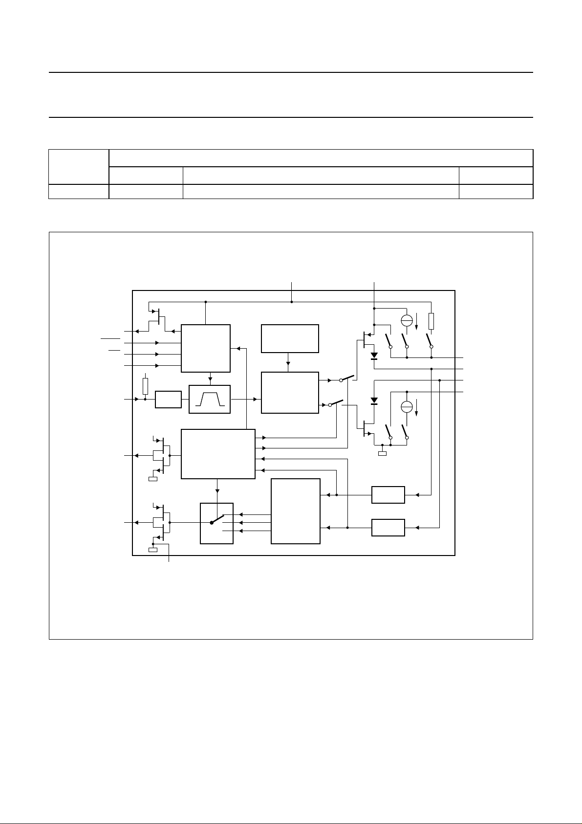
BLOCK DIAGRAM
handbook, full pagewidth
WAKE
STB
TXD
INH
EN
BAT
14
1
7
5
6
V
CC
2
TIMER
WAKE-UP
STANDBY
CONTROL
TEMPERATURE
PROTECTION
DRIVER
TJA1053
V
CC
10
12.5
kΩ
9
RTL
11
CANH
12
CANL
8
RTH
NERR
RXD
4
3
FAILURE DETECTOR
PLUS WAKE UP
PLUS TIME-OUT
13
GND
FILTER
RECEIVER
FILTER
MGL181
Fig.1 Block diagram.
1997 Oct 15 3
Philips Semiconductors Preliminary specification
Fault-tolerant CAN transceiver TJA1053
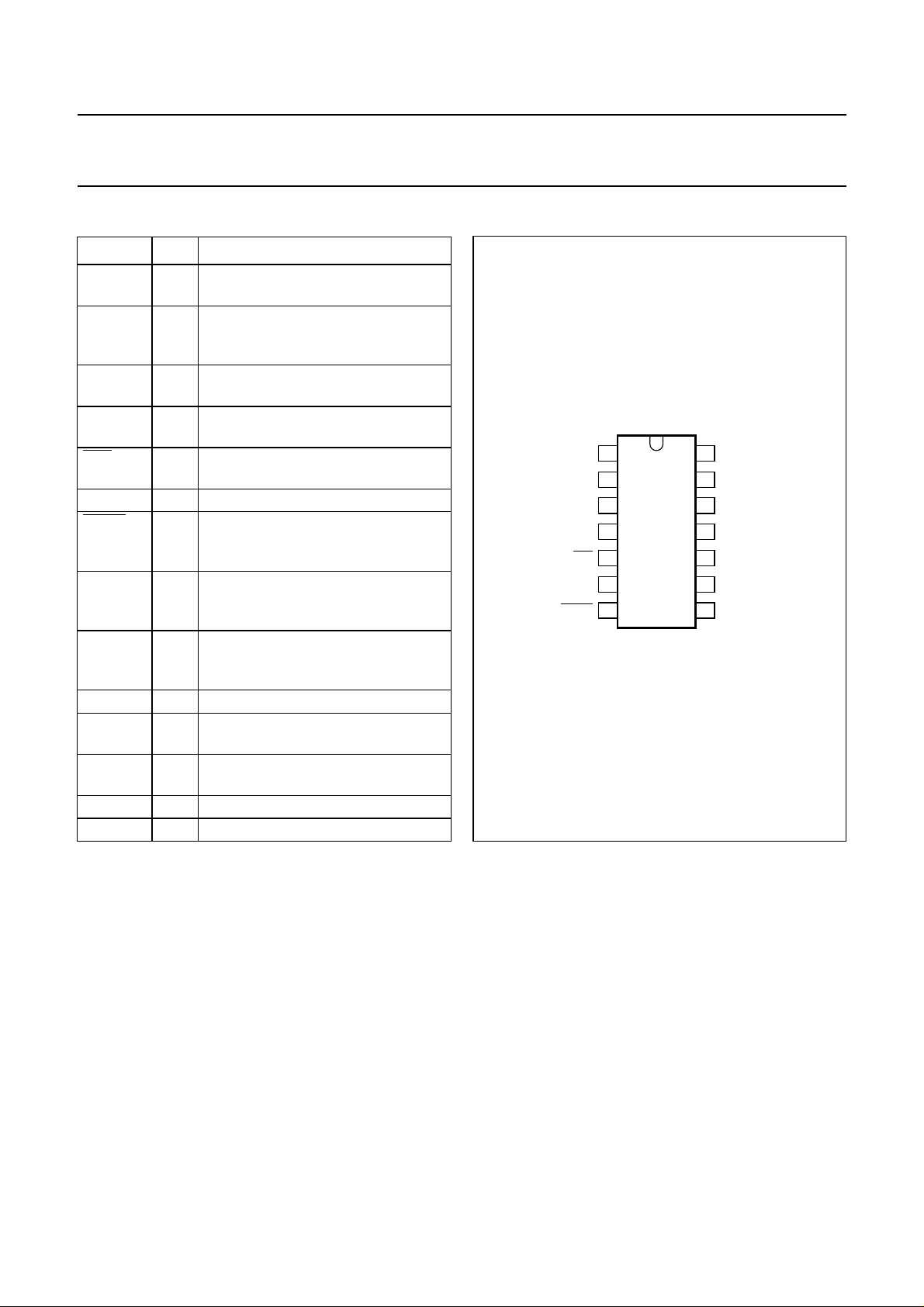
PINNING
SYMBOL PIN DESCRIPTION
INH 1 inhibit output for switching external
5 V regulator
TXD 2 transmit data input, when LOW bus
data will be dominant, when HIGH
bus data will be recessive
RXD 3 receive data output, when LOW bus
data will be dominant
NERR 4 error output pin, when LOW a bus
error exists
STB 5 not standby digital control input
signal (active LOW)
EN 6 enable digital control input signal
WAKE 7 not wake input signal, when pulled
down INH becomes active for
wake-up (active LOW)
RTH 8 termination resistor, CANH line will
be high-impedance with certain bus
errors
RTL 9 termination resistor, CANL line will be
high-impedance with certain bus
errors
V
CC
10 supply voltage (+5 V)
CANH 11 high voltage bus line, will be HIGH in
dominant state
CANL 12 low voltage bus line, will be LOW in
dominant state
GND 13 ground
BAT 14 battery voltage
handbook, halfpage
1INH
2
TXD GND
3
RXD CANL
4
NERR CANH
STB V
EN RTL
WAKE RTH
TJA1053T
5
6
7
MGL182
14 BAT
13
12
11
10
CC
9
8
Fig.2 Pin configuration.
1997 Oct 15 4

Philips Semiconductors Preliminary specification
Fault-tolerant CAN transceiver TJA1053
FUNCTIONAL DESCRIPTION
The TJA1053 is the interface between the CAN protocol
controller and the physical bus. It is primarily intended for
low speed applications, up to 125 kBaud, in passenger
cars. The device provides differential transmit capability to
the bus and differential receive capability to the CAN
controller.
To reduce RF interference the rise and fall slope are
limited. This allows the use of an unshielded twisted pair or
a parallel pair of wires for the bus. Moreover, it supports
transmission capability on either bus wire if one of the bus
wires is corrupted. The failure detection logic automatically
selects a suitable transmission mode.
In normal operation (no wiring failures) the differential
receiver is output to RXD. The differential receiver inputs
are connected to CANH and CANL through integrated
filters. The filtered input signals are also used for the single
wire receivers. The CANH and CANL receivers have
threshold voltages that ensure a maximum noise margin in
single-wire modes.
A timer has been integrated at the TXD input. This timer
prevents the TJA1053 to drive the bus lines to permanent
dominant state.
Failure detector
This time is needed to avoid false triggering by external RF
fields. Recovery from these failures is detected
automatically after a certain time-out (filtering) and no
transmission is lost. The CANH driver and the RTH pin are
switched off in the event of failure 3.
Failures 4 and 7 initially result in a permanent dominant
level at RXD. After a time-out, the CANL driver and the
RTL pin are switched off. Only a weak pull-up at RTL
remains. Reception continues by switching to the
single-wire mode via CANH. When failures 4 or 7 are
removed, the recessive bus levels are restored. If the
differential voltage remains below the recessive threshold
level for a certain period of time, reception and
transmission switch back to the differential mode.
If any of the seven wiring failures occur, the output NERR
will be made LOW. On error recovery, NERR will be made
HIGH again.
During all single-wire transmissions, the EMC
performance (both immunity and emission) is worse than
in the differential mode. Integrated receiver filters
suppress any HF noise induced into the bus wires.
The cut-off frequency of these filters is a compromise
between propagation delay and HF suppression. In the
single-wire mode, low frequency noise cannot be
distinguished from the required signal.
The failure detector is active in the normal operation mode
and detects the following single bus failures and switches
to an appropriate mode:
1. CANH wire interrupted
2. CANL wire interrupted
3. CANH short-circuited to battery
4. CANL short-circuited to ground
5. CANH short-circuited to ground
6. CANL short-circuited to battery
7. CANL mutually shorted to CANH.
The differential receiver threshold is set at −2.9 V.
This ensures correct reception in the normal operating
modes and, in the event of failures 1, 2 and 5 with a noise
margin as high as possible. These failures, or recovery
from them, do not destroy ongoing transmissions.
Failures 3 and 6 are detected by comparators connected
to CANH and CANL, respectively. If the comparator
threshold is exceeded for a certain period of time, the
reception is switched to the single-wire mode.
Low power modes
The transceiver provides 3 low power modes which can be
entered and exited via pins
STB and EN (see Table 1).
The sleep mode is the mode with the lowest power
consumption. The INH pin is switched to high-impedance
for deactivation of external voltage regulators. CANL is
biased to the battery voltage via the RTL output. If the
supply voltage is provided the RXD and NERR will signal
the wake-up interrupt
The V
standby mode will react the same as the sleep
BAT
mode with an active INH output.
The VCC standby mode is the V
standby with RTL
BAT
switched to the VCC voltage. In this mode the NERR output
signals the V
power-on flag and the RXD output will
BAT
show the wake-up interrupt.
1997 Oct 15 5
Philips Semiconductors Preliminary specification
Fault-tolerant CAN transceiver TJA1053
Wake-up requests are recognized by the transceiver when
a dominant signal is detected on either bus line or if the
WAKE pin is connected to ground. On a wake-up request
the transceiver will set the INH output which can be used
to activate the external VCC voltage regulator. If VCC is
provided the wake-up request can be read on the NERR or
RXD outputs, on which the external microcontroller can
wake up the transceiver (switch to normal operating mode)
via STB and EN.
To prevent false wake-up due to transients or RF fields,
wake-up voltage threshold levels have to be maintained
for a certain period of time. In the low power modes the
failure detection circuit remains partly active to prevent
increased power consumption should errors 3, 4 and 7
occur.
Power on
After power-on V
is switched on, the INH pin will
BAT
become HIGH and an internal power-on flag will be set.
This flag can be read via the NERR pin (STB = 1, EN = 0)
and will be reset by entering the normal operation mode.
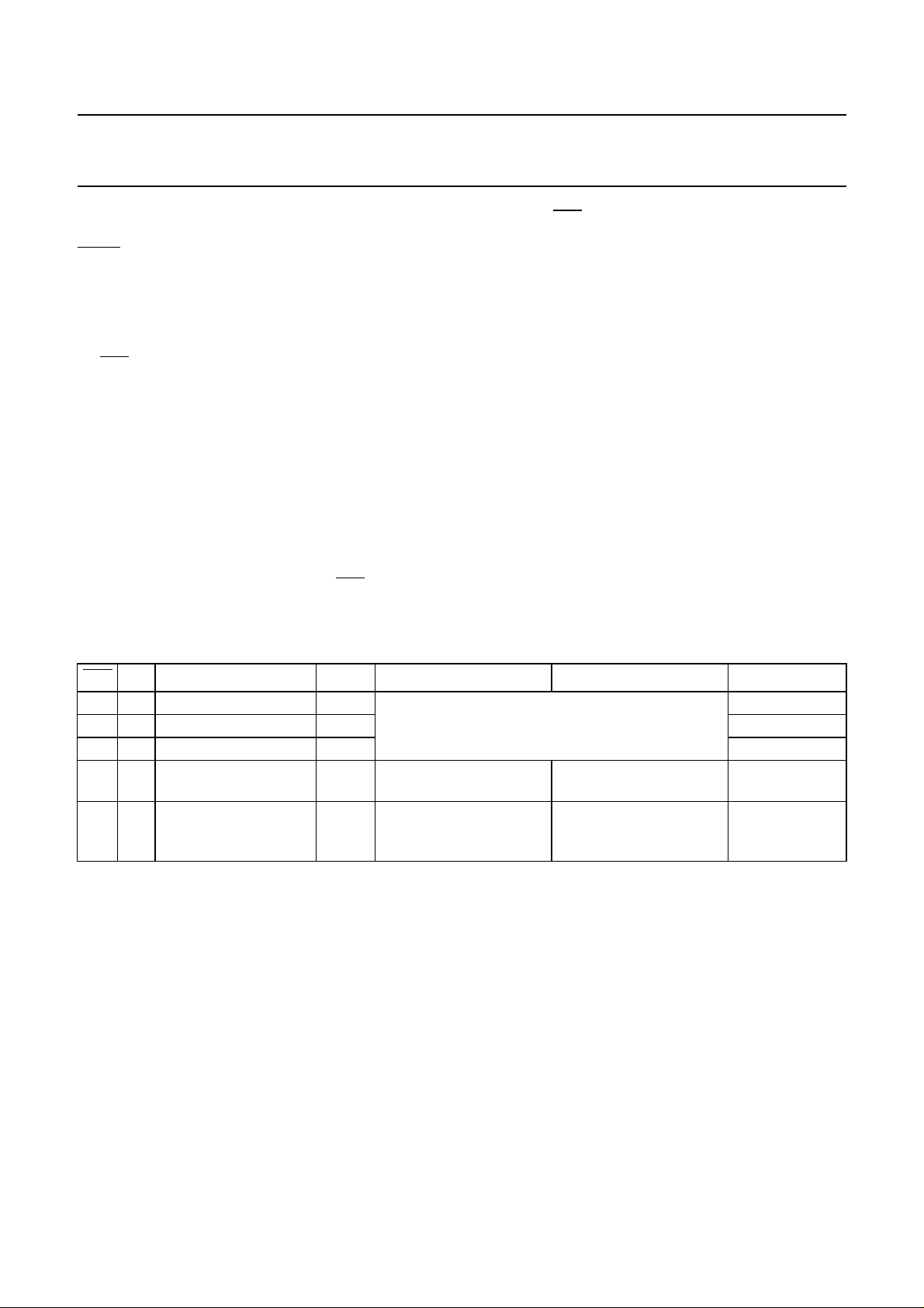
Table 1 Truth table of CAN transceiver
The EN and
STB pins will internally be set to LOW level, if
the VCC voltage is below a certain threshold level, to
provide fail safe functionality.
Protections
A current limiting circuit protects the transmitter output
stages against short-circuit to positive and negative
battery voltage.
If the junction temperature exceeds a maximum value, the
transmitter output stages are disabled. Because the
transmitter is responsible for the major part of the power
dissipation, this will result in a reduced power dissipation
and hence a lower chip temperature. All other parts of the
IC will remain operating.
The CANH and CANL inputs are protected against
electrical transients which may occur in an automotive
environment.
STB EN MODE INH NERR RXD RTL
00V
BAT
0 0 sleep
standby
(2)
(1)
HIGH active LOW wake-up interrupt signal if VCC is present switched to V
floating switched to V
0 1 go to sleep command floating switched to V
10VCC standby
1 1 normal operation mode HIGH active LOW error flag HIGH = receive;
(3)
HIGH active LOW V
power-on flag
BAT
active LOW wake-up
interrupt
switched to V
switched to V
LOW = dominant
received data
Notes
1. Wake-up interrupts are released when entering normal operating mode.
2. If go to sleep command was used before (EN may turn LOW as V
drops, without affecting internal functions
CC
because of fail safe functionality).
3. V
power-on flag will be reset when entering normal operation mode.
BAT
BAT
BAT
BAT
CC
CC
1997 Oct 15 6
 Loading...