

Page 1

查询TJA1041供应商
INTEGRATED CIRCUITS
DATA SH EET
TJA1041A
High speed CAN transceiver
Product specification
Supersedes data of 2003 Sep 29
2004 Feb 20
Page 2

Philips Semiconductors Product specification
High speed CAN transceiver TJA1041A
FEATURES
Optimized for in-vehicle high speed communication
• Fully compatible with the ISO 11898 standard
• Communication speed up to 1 Mbit/s
• Very low ElectroMagnetic Emission (EME)
• Differential receiver with wide common-mode range,
offering high ElectroMagnetic Immunity (EMI)
• Passive behaviour when supply voltage is off
• Automatic I/O-level adaptation to the host controller
supply voltage
• Recessive bus DC voltage stabilization for further
improvement of EME behaviour
• Listen-only mode for node diagnosis and failure
containment
• Allows implementation of large networks (more than
110 nodes).
Low-power management
• Very low-current in standby and sleep mode, with local
and remote wake-up
• Capability to power down the entire node, still allowing
local and remote wake-up
• Wake-up source recognition.
Protection and diagnosis (detection and signalling)
• TXD dominant clamping handler with diagnosis
• RXD recessive clamping handler with diagnosis
• TXD-to-RXD short-circuit handler with diagnosis
• Over-temperature protection with diagnosis
• Undervoltage detection on pins VCC, V
and V
I/O
BAT
• Automotive environment transient protected bus pins
and pin V
BAT
• Short-circuit proof bus pins and pin SPLIT (to battery
and to ground)
• Bus line short-circuit diagnosis
• Bus dominant clamping diagnosis
• Cold start diagnosis (first battery connection).
GENERAL DESCRIPTION
The TJA1041A provides an advanced interface between
the protocol controllerand the physical bus in a Controller
Area Network (CAN) node. The TJA1041A is primarily
intended for automotive high-speed CAN applications (up
to 1 Mbit/s). The transceiver provides differential transmit
capability to the bus and differential receive capability to
the CAN controller. The TJA1041A is fully compatible to
the ISO 11898 standard, and offers excellent EMC
performance, very low power consumption, and passive
behaviour when supply voltage is off. The advanced
features include:
• Low-power management, supporting local and remote
wake-up with wake-up source recognition and the
capability to control the power supply in the rest of the
node
• Several protection and diagnosis functions including
short circuits of the bus lines and first battery connection
• Automatic adaptation of the I/O-levels, in line with the
supply voltage of the controller.
ORDERING INFORMATION
TYPE
NUMBER
NAME DESCRIPTION VERSION
PACKAGE
TJA1041AT SO14 plastic small outline package; 14 leads; body width 3.9 mm SOT108-1
TJA1041AU − bare die; 1920 × 3190 × 380 µm −
2004 Feb 20 2
Page 3

Philips Semiconductors Product specification
High speed CAN transceiver TJA1041A
QUICK REFERENCE DATA
SYMBOL PARAMETER CONDITIONS MIN. MAX. UNIT
V
CC
V
I/O
V
BAT
I
BAT
V
CANH
V
CANL
V
SPLIT
V
esd
t
PD(TXD-RXD)
T
vj
DC voltage on pin V
DC voltage on pin V
DC voltage on pin V
V
input current V
BAT
CC
I/O
BAT
operating range 4.75 5.25 V
operating range 2.8 5.25 V
operating range 5 27 V
= 12 V 10 30 µA
BAT
DC voltage on pin CANH 0 < VCC< 5.25 V; no time limit −27 +40 V
DC voltage on pin CANL 0 < VCC< 5.25 V; no time limit −27 +40 V
DC voltage on pin SPLIT 0 < VCC< 5.25 V; no time limit −27 +40 V
electrostatic discharge voltage Human Body Model (HBM)
pins CANH, CANL and SPLIT −6+6kV
all other pins −4+4kV
propagation delay TXD to RXD V
= 0 V 40 255 ns
STB
virtual junction temperature −40 +150 °C
2004 Feb 20 3
Page 4
Philips Semiconductors Product specification
High speed CAN transceiver TJA1041A
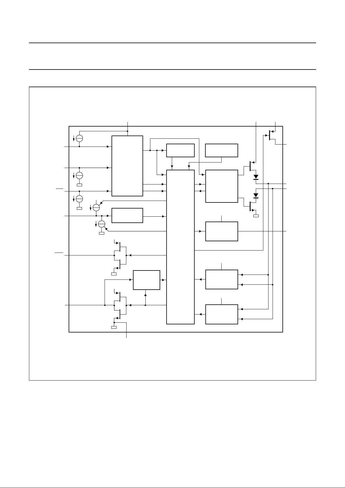
BLOCK DIAGRAM
handbook, full pagewidth
TXD
EN
STB
WAKE
ERR
RXD
V
I/O
5
V
CCVBAT
310
TJA1041A
1
TIME-OUT
6
14
V
BAT
9
8
4
LEVEL
ADAPTOR
WAKE
COMPARATOR
V
I/O
V
I/O
MODE
CONTROL
+
FAILURE
DETECTOR
+
WAKE-UP
DETECTOR
RXD
RECESSIVE
DETECTION
TEMPERATURE
PROTECTION
DRIVER
V
CC
SPLIT
V
BAT
LOW POWER
RECEIVER
V
CC
NORMAL
RECEIVER
7
INH
13
CANH
CANL
12
11
SPLIT
2
GND
Fig.1 Block diagram.
2004 Feb 20 4
MNB115
Page 5
Philips Semiconductors Product specification
High speed CAN transceiver TJA1041A
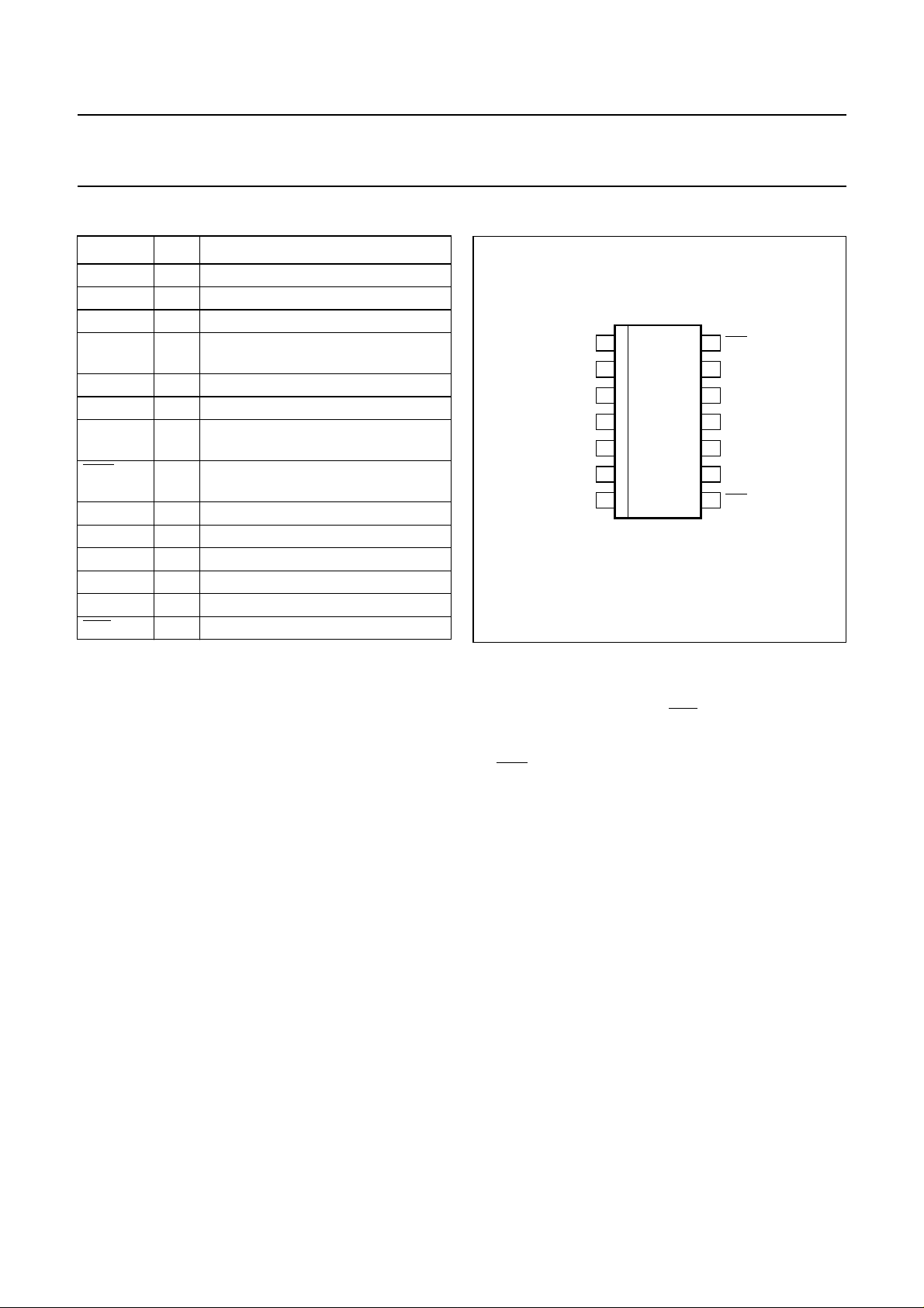
PINNING
SYMBOL PIN DESCRIPTION
TXD 1 transmit data input
GND 2 ground
V
CC
RXD 4 receive data output; reads out data
V
I/O
EN 6 enable control input
INH 7 inhibit output for switching external
ERR 8 error and power-on indication output
WAKE 9 local wake-up input
V
BAT
SPLIT 11 common-mode stabilization output
CANL 12 LOW-level CAN bus line
CANH 13 HIGH-level CAN bus line
STB 14 standby control input (active LOW)
3 transceiver supply voltage input
from the bus lines
5 I/O-level adapter voltage input
voltage regulators
(active LOW)
10 battery voltage input
handbook, halfpage
TXD
GND
V
CC
RXD
V
I/O
EN
INH
1
2
3
4
5
6
7
TJA1041AT
MDB635
STB
14
CANH
13
CANL
12
SPLIT
11
V
10
BAT
WAKE
9
ERR
8
Fig.2 Pinning configuration.
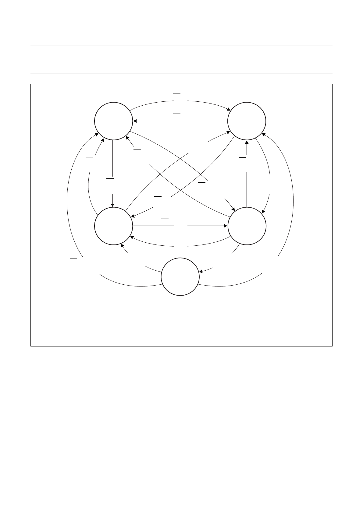
FUNCTIONAL DESCRIPTION
Theprimary function of a CAN transceiver is to provide the
CAN physical layer as described in the ISO 11898
standard. In the TJA1041A this primary function is
complemented with a number of operating modes,
fail-safe features and diagnosis features, which offer
enhanced system reliability and advanced power
management functionality.
Operating modes
The TJA1041A can be operated in five modes, each with
specific features. Control pins STB and EN select the
operating mode. Changing between modes also gives
access to a number of diagnostics flags, available via
pin ERR. The following sections describe the five
operating modes. Table 1 shows the conditions for
selecting these modes. Figure 3 illustrates the mode
transitions when VCC, V
and V
I/O
are present.
BAT
2004 Feb 20 5
Page 6

Philips Semiconductors Product specification
High speed CAN transceiver TJA1041A
Table 1 Operating mode selection
CONTROL PINS INTERNAL FLAGS
OPERATING MODE PIN INH
STB EN UV
NOM
X X set X X
UV
pwon, wake-up
BAT
(1)
sleep mode; note 2 floating
cleared set one or both set standby mode H
both cleared no change from sleep mode floating
standby mode from any other mode H
L L cleared cleared one or both set standby mode H
both cleared no change from sleep mode floating
standby mode from any other mode H
L H cleared cleared one or both set standby mode H
both cleared no change from sleep mode floating
go-to-sleep command mode from any
(3)
H
other mode; note 3
H L cleared cleared X pwon/listen-only mode H
H H cleared cleared X normal mode; note 4 H
Notes
1. Setting the pwon flag or the wake-up flag will clear the UV
2. The transceiver directly enters sleep mode and pin INH is set floating when the UV
undervoltage detection time on either VCC or V
has elapsed before that voltage level has recovered).
I/O
NOM
flag.
flag is set (so after the
NOM
3. When go-to-sleep command mode is selected for longer than the minimum hold time of the go-to-sleep command,
the transceiver will enter sleep mode and pin INH is set floating.
4. On entering normal mode the pwon flag and the wake-up flag will be cleared.
2004 Feb 20 6
Page 7
Philips Semiconductors Product specification
High speed CAN transceiver TJA1041A
handbook, full pagewidth
PWON/LISTEN-
ONLY MODE
STB = H
and
EN = L
(EN = L or flag set)
STANDBY
STB = H and EN = L
and
UV
cleared
NOM
STB = L
and
MODE
STB = H
and
EN = L
STB = L
and
flag set
STB = H
and
EN = H
STB = H
and
EN = L
STB = L
and
EN = L
STB = L and EN = H
and
flags cleared
STB = L
and
(EN = L or flag set)
SLEEP
MODE
STB = H
and
EN = H
STB = L and EN = H
and
flags cleared
flags cleared
t > t
GO-TO-SLEEP
and
h(min)
NORMAL
MODE
STB = H
and
EN = H
COMMAND
MODE
STB = L
and
EN = H
STB = H and EN = H
and
UV
cleared
NOM
LEGEND:
= H, = L
flag set
flags cleared
logical state of pin
setting pwon and/or wake-up flag
pwon and wake-up flag both cleared
Fig.3 Mode transitions when VCC, V
NORMAL MODE
Normal mode is the mode for normal bi-directional CAN
communication. The receiver will convert the differential
analog bus signal on pins CANH and CANL into digital
data, available for output to pin RXD. The transmitter will
convert digital data on pin TXD into a differential analog
signal, available for output to the bus pins. The bus pins
are biased at 0.5VCC (via R
). Pin INH is active, so
i(cm)
voltage regulators controlled by pin INH (see Fig.4) will be
active too.
PWON/LISTEN-ONLY MODE
In pwon/listen-only mode the transmitter of the transceiver
is disabled, effectively providing a transceiver listen-only
MGU983
and V
I/O
are present.
BAT
behaviour. The receiver will still convert the analog bus
signal on pins CANH and CANL into digital data, available
for output to pin RXD. As in normal mode the bus pins are
biased at 0.5VCC, and pin INH remains active.
STANDBY MODE
The standby mode is the first-level power saving mode of
the transceiver, offering reduced current consumption.
In standby mode the transceiver is not able to transmit or
receive data and the low-power receiver is activated to
monitor bus activity. The bus pins are biased at ground
level (via R
). Pin INH is still active, so voltage
i(cm)
regulators controlled by this pin INH will be active too.
2004 Feb 20 7
Page 8

Philips Semiconductors Product specification
High speed CAN transceiver TJA1041A
Pins RXD and ERR will reflect any wake-up requests
(provided that V
and VCC are present).
I/O
command mode, and also when the undervoltage
detection time on either VCC or V
voltagelevel has recovered. In sleep modethe transceiver
GO-TO-SLEEP COMMAND MODE
The go-to-sleep command mode is the controlled route for
entering sleep mode. In go-to-sleep command mode the
transceiver behaves as if in standby mode, plus a
go-to-sleep command is issued to the transceiver. After
remaining in go-to-sleep command mode for the minimum
hold time (t
), the transceiver will enter sleep mode.
h(min)
The transceiver will not enter the sleep mode if the state of
pins STB or EN is changed or the UV
wake-up flag is set before t
has expired.
h(min)
, pwon or
BAT
still behaves as described for standby mode, but now
pin INH is set floating. Voltage regulators controlled by
pin INH will be switched off, and the current into pin V
is reduced to a minimum. Waking up a node from sleep
mode is possible via the wake-up flag and (as long as the
UV
NOM
Internal flags
The TJA1041A makes use of seven internal flags for its
fail-safe fallback mode control and system diagnosis
support. Table 1 shows the relation between flags and
SLEEP MODE
The sleep mode is the second-level power saving mode of
the transceiver. Sleep mode is entered via the go-to-sleep
operating modes of the transceiver. Five of the internal
flags can be made available to the controller via pin ERR.
Table 2 shows the details on how to access these flags.
The following sections describe the seven internal flags.
Table 2 Accessing internal flags via pin ERR
Internal flag Flag is available on pin ERR
UV
UV
NOM
BAT
no by setting the pwon or wake-up flag
no when V
(1)
pwon in pwon/listen-only mode (coming from standby
mode, go-to-sleep command mode, or sleep mode)
wake-up in standby mode, go-to-sleep command mode, and
sleep mode (provided that V
and VCCare present)
I/O
wake-up source in normal mode (before the fourth dominant to
recessive edge on pin TXD; note 2)
bus failure in normal mode (after the fourth dominant to
recessive edge on pin TXD; note 2)
local failure in pwon/listen-only mode (coming from normal
mode)
elapses before that
I/O
flag is not set) via pin STB.
Flag is cleared
has recovered
BAT
on entering normal mode
on entering normal mode, or by setting the
pwon or UV
NOM
flag
on leaving normal mode, or by setting the
pwon flag
on re-entering normal mode
on entering normal mode or when RXD is
dominant while TXD is recessive (provided
that all local failures are resolved)
BAT
Notes
1. Pin ERRis an active-LOW output, so aLOW level indicates a set flaganda HIGH level indicates a clearedflag. Allow
pin ERR to stabilize for at least 8 µs after changing operating modes.
2. Allow for a TXD dominant time of at least 4 µs per dominant-recessive cycle.
2004 Feb 20 8
Page 9

Philips Semiconductors Product specification
High speed CAN transceiver TJA1041A
UV
UV
FLAG
NOM
is the VCC and V
NOM
undervoltage detection flag.
I/O
The flag is set when the voltage on pin VCC drops below
V
CC(sleep)
pin V
When the UV
for longer than t
drops below V
I/O
NOM
or when the voltage on
UV(VCC)
I/O(sleep)
for longer than t
UV(VI/O)
flag is set, the transceiver will enter
.
sleepmodetosavepowerandnotdisturbthebus.In sleep
mode the voltage regulators connected to pin INH are
disabled, avoiding the extra power consumption in case of
a short-circuit condition. After a waiting time (fixed by the
sametimers used for setting UV
or setting of the pwon flag will clear UV
)any wake-up request
NOM
and the timers,
NOM
allowing the voltage regulators to be reactivated at least
until UV
UV
BAT
UV
BAT
set when the voltage on pin V
WhenUV
mode to save power and not disturb the bus. UV
cleared when the voltage on pin V
is set again.
NOM
FLAG
is the V
BAT
undervoltage detection flag. The flag is
BAT
drops below V
BAT
isset, the transceiver will tryto enter standby
has recovered. The
BAT
BAT(stb)
is
BAT
.
transceiver will then return to the operating mode
determined by the logic state of pins STB and EN.
PWON FLAG
Pwon is the V
voltage on pin V
V
BAT(pwon)
, particularly after the transceiver was
power-on flag. This flag is set when the
BAT
has recovered after it dropped below
BAT
disconnected from the battery. By setting the pwon flag,
the UV
flag and timers are cleared and the transceiver
NOM
cannot enter sleep mode. This ensures that any voltage
regulator connected to pin INH is activated when the node
isreconnectedto the battery. In pwon/listen-only mode the
pwon flag can be made available on pin ERR. The flag is
cleared when the transceiver enters normal mode.
WAKE-UP FLAG
The wake-up flag is set when the transceiver detects a
local or a remote wake-up request. A local wake-up
request is detected when a logic state change on
pin WAKE remains stable for at least t
. A remote
wake
wake-uprequest is detected after two busdominant states
of at least t
BUSdom
recessive state of at least t
(with each dominant state followed by a
). The wake-up flag can
BUSrec
only be set in standby mode, go-to-sleep command mode
or sleep mode. Setting of the flag is blocked during the
UV
flag waiting time. By setting the wake-up flag, the
NOM
UV
flag and timers are cleared. The wake-up flag is
NOM
immediately available on pins ERR and RXD (provided
that V
power-on, or when theUV
and VCC are present). The flag is cleared at
I/O
flag is set orthe transceiver
NOM
enters normal mode.
WAKE-UP SOURCE FLAG
Wake-up source recognition is provided via the wake-up
source flag, which is set when the wake-up flag is set by a
local wake-up request via pin WAKE.The wake-up source
flag can only be set after the pwon flag is cleared.
In normal mode the wake-up source flag can be made
available on pin ERR. The flag is cleared at power-on or
when the transceiver leaves normal mode.
BUS FAILURE FLAG
The bus failure flag is set if the transceiver detects a bus
line short-circuit condition to V
BAT,VCC
or GND during four
consecutive dominant-recessive cycles on pin TXD, when
trying to drive the bus lines dominant. In normal mode the
bus failure flag can be made available on pin ERR. The
flag is cleared when the transceiver re-enters normal
mode.
LOCAL FAILURE FLAG
In normal mode or pwon/listen-only mode the transceiver
can recognize five different local failures, and will combine
them into one local failure flag. The five local failures are:
TXD dominant clamping, RXD recessive clamping, a
TXD-to-RXD short circuit, bus dominant clamping, and
over-temperature. Nature and detection of these local
failures is described in Section “Local failures”.
In pwon/listen-onlymodethelocalfailureflagcanbemade
available on pin ERR. The flag is cleared when entering
normal mode or when RXD is dominant while TXD is
recessive, provided that all local failures are resolved.
Local failures
The TJA1041A can detect five different local failure
conditions. Any of these failures will set the local failure
flag, and in most cases the transmitter of the transceiver
will be disabled. The following sections give the details.
TXD DOMINANT CLAMPING DETECTION
A permanent LOW level on pin TXD (due to a hardware or
software application failure) would drive the CAN bus into
a permanent dominant state, blocking all network
communication. The TXD dominant time-out function
prevents such a network lock-up by disabling the
transmitter of the transceiver if pin TXD remains at a LOW
level for longer than the TXD dominant time-out t
dom(TXD)
.
2004 Feb 20 9
Page 10

Philips Semiconductors Product specification
High speed CAN transceiver TJA1041A
The t
dom(TXD)
timer defines the minimum possible bit rate
of 40 kbit/s. The transmitter remains disabled until the
local failure flag is cleared.
RXD RECESSIVE CLAMPING DETECTION
An RXD pin clamped to HIGH level will prevent the
controller connected to this pin from recognizing a bus
dominant state. So the controller can start messages at
any time, which is likely to disturb all bus communication.
RXD recessive clamping detection prevents this effect by
disabling the transmitter when the bus is in dominant state
without RXD reflecting this. The transmitter remains
disabled until the local failure flag is cleared.
TXD-TO-RXD SHORT-CIRCUIT DETECTION
Ashort-circuitbetweenpins RXDand TXDwouldkeepthe
bus in a permanent dominant state once the bus is driven
dominant, because the low-side driver of RXD is typically
stronger than the high-side driver of the controller
connected to TXD. The TXD-to-RXD short-circuit
detectionpreventssuch a network lock-up by disabling the
transmitter.Thetransmitterremainsdisableduntilthe local
failure flag is cleared.
BUS DOMINANT CLAMPING DETECTION
A CAN bus short circuit (to V
BAT,VCC
or GND) or a failure
in one of the other network nodes could result in a
differential voltage on the bus high enough to represent a
bus dominant state. Because a node will not start
transmission if the bus is dominant, the normal bus failure
detection will not detect this failure, but the bus dominant
clamping detection will. The local failure flag is set if the
dominantstate on the bus persists for longer thant
dom(bus)
By checking this flag, the controller can determine if a
clamped bus is blocking network communication. There is
no need to disable the transmitter. Note that the local
failure flag does not retain a bus dominant clamping
failure, and is released as soon as the bus returns to
recessive state.
OVER-TEMPERATURE DETECTION
To protect the output drivers of the transceiver against
overheating, the transmitter will be disabled if the virtual
junction temperature exceeds the shutdown junction
temperature T
. The transmitter remains disabled until
j(sd)
the local failure flag is cleared.
Recessive bus voltage stabilization
In recessive state the output impedance of transceivers is
relatively high. In a partially powered network (supply
voltage is off in some of the nodes) any deactivated
transceiver with a significant leakage current is likely to
load the recessive bus to ground. This will cause a
common-modevoltagestepeachtimetransmissionstarts,
resulting in increased ElectroMagnetic Emission (EME).
Using pin SPLIT of the TJA1041A in combination with split
termination (see Fig.5) will reduce this step effect. In
normal mode and pwon/listen-only mode pin SPLIT
providesastabilized0.5VCCDC voltage.Instandbymode,
go-to-sleep command mode and sleep mode pin SPLIT is
set floating.
I/O level adapter
The TJA1041A is equipped with a built-in I/O-level
adapter.Byusingthesupplyvoltageofthecontroller(tobe
supplied at pin V
) the level adapter ratio-metrically
I/O
scalestheI/O-levels of the transceiver. For pins TXD, STB
and EN the digital input threshold level is adjusted, and for
pins RXD and ERR the HIGH-level output voltage is
adjusted. This allows the transceiver to be directly
interfaced with controllers on supply voltages between
2.8 V and 5.25 V, without the need for glue logic.
Pin WAKE
Pin WAKE of the TJA1041A allows local wake-up
.
triggering by a LOW to HIGH state change as well as a
HIGHto LOW state change. This gives maximum flexibility
when designing a local wake-up circuit. To keep current
consumption at a minimum, after a t
delay the internal
wake
bias voltage of pin WAKE will follow the logic state of this
pin. A HIGH level on pin WAKE is followed by an internal
pull-up to V
. A LOW level on pin WAKE is followed by
BAT
an internal pull-down towards GND. To ensure EMI
performance in applications not using local wake-up it is
recommended to connect pin WAKE to pin V
BAT
GND.
or to pin
2004 Feb 20 10
Page 11

Philips Semiconductors Product specification
High speed CAN transceiver TJA1041A
LIMITING VALUES
In accordance with the Absolute Maximum Rating System (IEC 60134).
SYMBOL PARAMETER CONDITIONS MIN. MAX. UNIT
V
CC
V
I/O
V
BAT
V
TXD
V
RXD
V
STB
V
EN
V
ERR
V
INH
V
WAKE
I
WAKE
V
CANH
V
CANL
V
SPLIT
V
trt
V
esd
T
vj
T
stg
DC voltage on pin V
CC
no time limit −0.3 +6 V
operating range 4.75 5.25 V
DC voltage on pin V
I/O
no time limit −0.3 +6 V
operating range 2.8 5.25 V
DC voltage on pin V
BAT
no time limit −0.3 +40 V
operating range 5 27 V
load dump − 40 V
DC voltage on pin TXD −0.3 V
DC voltage on pin RXD −0.3 V
DC voltage on pin STB −0.3 V
DC voltage on pin EN −0.3 V
DC voltage on pin ERR −0.3 V
DC voltage on pin INH −0.3 V
DC voltage on pin WAKE −0.3 V
+ 0.3 V
I/O
+ 0.3 V
I/O
+ 0.3 V
I/O
+ 0.3 V
I/O
+ 0.3 V
I/O
+ 0.3 V
BAT
+ 0.3 V
BAT
DC current on pin WAKE −−15 mA
DC voltage on pin CANH 0 < VCC< 5.25 V; no time limit −27 +40 V
DC voltage on pin CANL 0 < VCC< 5.25 V; no time limit −27 +40 V
DC voltage on pin SPLIT 0 < VCC< 5.25 V; no time limit −27 +40 V
transient voltages on pins CANH,
CANL, SPLIT and V
BAT
according to ISO 7637; see Fig.6 −200 +200 V
electrostatic discharge voltage Human Body Model (HBM);
note 1
pins CANH, CANL and SPLIT −6+6kV
all other pins −4+4kV
Machine Model (MM); note 2 −200 +200 V
virtual junction temperature note 3 −40 +150 °C
storage temperature −55 +150 °C
Notes
1. Equivalent to discharging a 100 pF capacitor via a 1.5 kΩ series resistor (6 kV level with pin GND connected to
ground).
2. Equivalent to discharging a 200 pF capacitor via a 0.75 µH series inductor and a 10 Ω series resistor.
3. Junction temperature in accordance with IEC 60747-1. An alternative definition is: Tvj=T
R
th(vj-amb)
temperature (T
is a fixed value. The rating for Tvj limits the allowable combinations of power dissipation (P) and ambient
).
amb
amb
+P× R
th(vj-amb)
, where
THERMAL CHARACTERISTICS
SYMBOL PARAMETER CONDITIONS VALUE UNIT
R
R
th(j-a)
th(j-s)
thermal resistance from junction to ambient in SO14 package in free air 120 K/W
thermal resistance from junction to substrate of bare die in free air 40 K/W
2004 Feb 20 11
Page 12

Philips Semiconductors Product specification
High speed CAN transceiver TJA1041A
QUALITY SPECIFICATION
Quality specification in accordance with
“AEC-Q100”
.
CHARACTERISTICS
VCC= 4.75 V to 5.25 V; V
= 2.8 V to VCC; V
I/O
=5Vto27V; RL=60Ω; Tvj= −40 °C to +150 °C; unless specified
BAT
otherwise; all voltages are defined with respect to ground; positive currents flow into the device; note 1.
SYMBOL PARAMETER CONDITIONS MIN. TYP. MAX. UNIT
Supplies (pins V
V
CC(sleep)
, VCC and V
BAT
VCC undervoltage detection
I/O
)
V
= 12 V (fail-safe) 2.75 3.3 4.5 V
BAT
level for forced sleep mode
V
I/O(sleep)
V
undervoltage detection
I/O
0.5 1.5 2 V
level for forced sleep mode
V
BAT(stb)
V
voltage levelforfail-safe
BAT
VCC= 5 V (fail-safe) 2.75 3.3 4.5 V
fallback mode
V
BAT(pwon)
V
voltage level for setting
BAT
VCC= 0 V 2.5 3.3 4.1 V
pwon flag
I
CC
VCC input current normal mode; V
TXD
=0V
25 55 80 mA
(dominant)
normal or pwon/listen-only
mode; V
TXD=VI/O
2 6 10 mA
(recessive)
standby or sleep mode − 110µA
I
I/O
V
input current normal mode; V
I/O
TXD
=0V
100 350 1000 µA
(dominant)
normal or pwon/listen-only
mode; V
TXD=VI/O
15 80 200 µA
(recessive)
standby or sleep mode − 05µA
I
BAT
V
input current normal or pwon/listen-only
BAT
15 30 40 µA
mode
standby mode;
VCC> 4.75 V; V
V
INH=VWAKE=VBAT
sleep mode;
V
INH=VCC=VI/O
V
WAKE=VBAT
=12V
= 2.8 V;
I/O
=0V;
=12V
10 20 30 µA
10 20 30 µA
Transmitter data input (pin TXD)
V
IH
V
IL
I
IH
I
IL
C
i
HIGH-level input voltage 0.7V
LOW-level input voltage −0.3 − 0.3V
HIGH-level input current normal or pwon/listen-only
mode; V
TXD=VI/O
LOW-level input current normal or pwon/listen-only
mode; V
TXD
= 0.3V
I/O
−50 +5 µA
−70 −250 −500 µA
− VCC+ 0.3 V
I/O
I/O
input capacitance not tested − 510pF
V
2004 Feb 20 12
Page 13

Philips Semiconductors Product specification
High speed CAN transceiver TJA1041A
SYMBOL PARAMETER CONDITIONS MIN. TYP. MAX. UNIT
Receiver data output (pin RXD)
I
OH
I
OL
Standby and enable control inputs (pins STB and EN)
V
IH
V
IL
I
IH
I
IL
Error and power-on indication output (pin ERR)
I
OH
I
OL
Local wake-up input (pin WAKE)
I
IH
I
IL
V
th
Inhibit output (pin INH)
∆V
H
IL leakage current sleep mode − 05µA
Bus lines (pins CANH and CANL)
V
O(dom)
V
O(dom)(m)
V
O(dif)(bus)
V
O(reces)
I
O(sc)
I
O(reces)
HIGH-level output current V
LOW-level output current V
RXD=VI/O
V
I/O=VCC
RXD
− 0.4 V;
= 0.4 V; V
TXD=VI/O
−1 −3 −6mA
;
2 5 12 mA
bus dominant
HIGH-level input voltage 0.7V
− VCC+ 0.3 V
I/O
LOW-level input voltage −0.3 − 0.3V
HIGH-level input current V
LOW-level input current V
HIGH-level output current V
LOW-level output current V
HIGH-level input current V
LOW-level input current V
threshold voltage V
HIGH-level voltage drop I
dominant output voltage V
STB=VEN
STB=VEN
ERR=VI/O
V
I/O=VCC
ERR
WAKE=VBAT
WAKE=VBAT
STB
= −0.18 mA 0.05 0.2 0.8 V
INH
TXD
= 0.7V
I/O
14 10µA
=0V − 0 −1 µA
− 0.4 V;
−4 −20 −50 µA
= 0.4 V 0.1 0.2 0.35 mA
− 1.9 V −1 −5 −10 µA
− 3.1 V 1 5 10 µA
=0V V
BAT
− 3V
BAT
− 2.5 V
BAT
=0V
pin CANH 3 3.6 4.25 V
pin CANL 0.5 1.4 1.75 V
matching of dominant output
−0.1 − +0.15 V
voltage
(VCC− V
differentialbusoutputvoltage
(V
CANH
CANH
− V
CANL
− V
)
CANL
)
V
= 0 V (dominant);
TXD
1.5 − 3.0 V
45 Ω <RL<65Ω
V
TXD=VI/O
(recessive); no
−50 − +50 mV
load
recessive output voltage normal or pwon/listen-only
mode; V
TXD=VI/O
; no load
standby or sleep mode; no
2 0.5V
CC
3V
−0.1 0 +0.1 V
load
short-circuit output current V
recessive output current −27V<V
= 0 V (dominant)
TXD
pin CANH; V
pin CANL; V
CAN
=0 −40 −70 −95 mA
CANH
= 40 V 40 70 95 mA
CANL
<32V −2.5 − +2.5 mA
V
I/O
− 2V
2004 Feb 20 13
Page 14

Philips Semiconductors Product specification
High speed CAN transceiver TJA1041A
SYMBOL PARAMETER CONDITIONS MIN. TYP. MAX. UNIT
V
dif(th)
V
hys(dif)
I
LI
R
i(cm)
R
i(cm)(m)
R
i(dif)
C
i(cm)
C
i(dif)
R
sc(bus)
Common-mode stabilization output (pin SPLIT)
V
o
IL leakage current standby or sleep mode;
Timing characteristics; see Figs 8 and 9
t
d(TXD-BUSon)
t
d(TXD-BUSoff)
t
d(BUSon-RXD)
t
d(BUSoff-RXD)
t
PD(TXD-RXD)
t
t
t
t
UV(VCC)
UV(VI/O)
dom(TXD)
dom(bus)
,
differential receiver threshold
voltage
differential receiver
hysteresis voltage
input leakage current VCC=0V
common-mode input
normal or pwon/listen-only
mode (see Fig.7);
−12V<V
−12V<V
CANH
CANL
<12V;
<12V
standby or sleep mode;
−12V<V
−12V<V
CANH
CANL
<12V;
<12V
normal or pwon/listen-only
mode (see Fig.7);
−12V<V
−12V<V
V
CANH=VCANL
CANH
CANL
<12V;
<12V
=5V
0.5 0.7 0.9 V
0.4 0.7 1.15 V
50 70 100 mV
100 170 250 µA
15 25 35 kΩ
resistance
common-mode input
V
CANH=VCANL
−3 0 +3 %
resistance matching
differential input resistance 25 50 75 kΩ
common-mode input
V
TXD=VCC
; not tested −− 20 pF
capacitance
differential input capacitance V
detectable short-circuit
TXD=VCC
normal mode 0 − 50 Ω
; not tested −− 10 pF
resistance between bus lines
and V
output voltage normal or pwon/listen-only
, VCC and GND
BAT
0.3V
CC
0.5V
CC
0.7V
CC
V
mode;
−500 µA<I
SPLIT
< 500 µA
− 05µA
−22V<V
SPLIT
<35V
delay TXD to bus active normal mode 25 70 110 ns
delay TXD to bus inactive normal mode 10 50 95 ns
delay bus active to RXD normal or pwon/listen-only
15 65 115 ns
mode
delay bus inactive to RXD normal or pwon/listen-only
35 100 160 ns
mode
propagation delay TXD to
V
=0V 40 − 255 ns
STB
RXD
undervoltage detection time
on VCC and V
I/O
TXD dominant time-out V
bus dominant time-out V
= 0 V 300 600 1000 µs
TXD
> 0.9 V 300 600 1000 µs
dif
5 10 12.5 ms
2004 Feb 20 14
Page 15

Philips Semiconductors Product specification
High speed CAN transceiver TJA1041A
SYMBOL PARAMETER CONDITIONS MIN. TYP. MAX. UNIT
t
h(min)
t
BUSdom
t
BUSrec
t
wake
Thermal shutdown
T
j(sd)
Note
1. All parameters are guaranteed over the virtual junction temperature range by design, but only 100 % tested at
T
= 125 °Cfordieson waferleveland in additionto this,100 % tested at T
amb
specified otherwise. For bare dies, all parameters are only guaranteed with the reverse side of the die connected to
ground.
minimum hold time of
go-to-sleep command
dominant time for wake-up
via bus
recessive time for wake-up
via bus
minimum wake-up time after
receiving a falling or rising
edge
shutdown junction
temperature
standby or sleep mode;
V
=12V
BAT
standby or sleep mode;
V
=12V
BAT
standby or sleep mode;
V
=12V
BAT
20 35 50 µs
0.75 1.75 5 µs
0.75 1.75 5 µs
52550µs
155 165 180 °C
= 125 °Cforcasedproducts,unless
amb
TEST AND APPLICATION INFORMATION
handbook, full pagewidth
BAT
WAKE
GND
V
BAT
TJA1041A
CAN bus wires
5 V
INH
SPLIT
3 V
V
CC
V
I/O
V
STB
EN
ERR
RXD
TXD
CANLCANH
CC
Port x, y, z
MICRO-
CONTROLLER
RXD
TXD
MNB116
Fig.4 Typical application with 3 V microcontroller.
2004 Feb 20 15
Page 16

Philips Semiconductors Product specification
High speed CAN transceiver TJA1041A
handbook, full pagewidth
handbook, full pagewidth
V
= 0.5V
SPLIT
in normal mode
and pwon/listen-only
otherwise floating
CC
mode;
Fig.5 Stabilization circuitry and application.
V
CC
R
R
GND
TJA1041A
+
12 V
CANH
SPLIT
CANL
60 Ω
60 Ω
V
SPLIT
MNB117
+
5 V
100 nF47 µF
5
TXD
1
EN
6
STB
14
WAKE
9
500 kHz
The waveforms of the applied transients will be in accordance with ISO 7637 part 1, test pulses 1, 2, 3a, 3b, 5, 6 and 7.
VCCV
V
I/O
310
TJA1041A
2
GND
BAT
13
12
11
8
7
4
CANH
CANL
SPLIT
ERR
INH
RXD
10 µF
1 nF
1 nF
MNB118
Fig.6 Test circuit for automotive transients.
2004 Feb 20 16
TRANSIENT
GENERATOR
Page 17

Philips Semiconductors Product specification
High speed CAN transceiver TJA1041A
handbook, full pagewidth
handbook, full pagewidth
V
RXD
hysteresis
0.5 0.9
Fig.7 Hysteresis of the receiver.
+
12 V
V
i(dif)(bus)
MGS378
HIGH
LOW
(V)
+
5 V
100 nF47 µF
TXD
EN
STB
WAKE
1
6
14
9
V
I/O
5
TJA1041A
Fig.8 Test circuit for timing characteristics.
2004 Feb 20 17
V
CCVBAT
310
13
12
11
8
7
4
2
GND
CANH
CANL
SPLIT
ERR
INH
RXD
10 µF
15 pF
R
L
60 Ω
MNB119
C
L
100 pF
Page 18

Philips Semiconductors Product specification
High speed CAN transceiver TJA1041A
handbook, full pagewidth
(1) V
i(dif)(bus)=VCANH
− V
CANL
.
TXD
CANH
CANL
V
i(dif)(bus)
RXD
t
d(TXD-BUSon)
t
d(BUSon-RXD)
(1)
t
PD(TXD-RXD
0.3V
CC
)
t
PD(TXD-RXD
Fig.9 Timing diagram.
0.9 V
0.5 V
0.7V
t
d(TXD-BUSoff)
t
d(BUSoff-RXD)
)
HIGH
LOW
dominant
(BUS on)
recessive
(BUS off)
HIGH
CC
LOW
MGS377
BONDING PAD LOCATIONS
COORDINATES
(1)
SYMBOL PAD
xy
TXD 1 664.25 3004.5
GND 2 75.75 3044.25
V
CC
3 115.5 2573
RXD 4 115.5 1862.75
V
I/O
5 115.5 115.5
EN 6 264.5 114
INH 7 667.75 85
ERR 8 1076.75 115.5
WAKE 9 1765 85
V
BAT
10 1765 792.5
SPLIT 11 1765 1442.25
CANL 12 1765 2115
CANH 13 1751 3002.5
STB 14 940.75 3004.5
Note
1. All x/y coordinates represent the position of the centre
ofeachpad(inµm)withrespecttothelefthandbottom
corner of the top aluminium layer.
handbook, halfpage
The reverse side of the bare die must be connected to ground.
2
3
4
5
x
0
678
0
y
141
TJA1041AU
13
12
11
10
9
MDB634
Fig.10 Bonding pad locations.
2004 Feb 20 18
Page 19

Philips Semiconductors Product specification
High speed CAN transceiver TJA1041A
PACKAGE OUTLINE
SO14: plastic small outline package; 14 leads; body width 3.9 mm
D
c
y
Z
14
pin 1 index
1
e
8
A
2
7
w
b
p
M
SOT108-1
E
H
E
A
1
detail X
A
X
v
M
A
Q
(A )
L
p
L
A
3
θ
0 2.5 5 mm
scale
DIMENSIONS (inch dimensions are derived from the original mm dimensions)
mm
OUTLINE
VERSION
SOT108-1
A
max.
1.75
0.069
A1A2A
0.25
1.45
0.10
1.25
0.010
0.057
0.004
0.049
IEC JEDEC JEITA
076E06 MS-012
0.25
0.01
b
3
p
0.49
0.36
0.019
0.0100
0.014
0.0075
UNIT
inches
Note
1. Plastic or metal protrusions of 0.15 mm (0.006 inch) maximum per side are not included.
cD
0.25
8.75
0.19
8.55
0.35
0.34
REFERENCES
(1)E(1)
4.0
3.8
0.16
0.15
eHELLpQZywv θ
1.27
0.05
2004 Feb 20 19
6.2
5.8
0.244
0.228
1.05
0.041
1.0
0.4
0.039
0.016
0.7
0.25
0.6
0.028
0.01 0.004
0.024
EUROPEAN
PROJECTION
0.25 0.1
0.01
(1)
0.7
0.3
0.028
0.012
ISSUE DATE
99-12-27
03-02-19
o
8
o
0
Page 20

Philips Semiconductors Product specification
High speed CAN transceiver TJA1041A
SOLDERING
Introduction to soldering surface mount packages
Thistextgivesaverybriefinsighttoacomplextechnology.
A more in-depth account of soldering ICs can be found in
our
“Data Handbook IC26; Integrated Circuit Packages”
(document order number 9398 652 90011).
There is no soldering method that is ideal for all surface
mount IC packages. Wave soldering can still be used for
certainsurfacemountICs,butitisnotsuitableforfinepitch
SMDs. In these situations reflow soldering is
recommended.
Reflow soldering
Reflow soldering requires solder paste (a suspension of
fine solder particles, flux and binding agent) to be applied
totheprinted-circuit board by screen printing, stencilling or
pressure-syringe dispensing before package placement.
Driven by legislation and environmental forces the
worldwide use of lead-free solder pastes is increasing.
Several methods exist for reflowing; for example,
convection or convection/infrared heating in a conveyor
type oven. Throughput times (preheating, soldering and
cooling) vary between 100 and 200 seconds depending
on heating method.
Typical reflow peak temperatures range from
215 to 270 °C depending on solder paste material. The
top-surface temperature of the packages should
preferably be kept:
• below 225 °C (SnPb process) or below 245 °C (Pb-free
process)
– for all BGA, HTSSON-T and SSOP-T packages
– for packages with a thickness ≥ 2.5 mm
– for packages with a thickness < 2.5 mm and a
volume ≥ 350 mm3 so called thick/large packages.
• below 240 °C (SnPb process) or below 260 °C (Pb-free
process) for packages with a thickness < 2.5 mm and a
volume < 350 mm3 so called small/thin packages.
Moisture sensitivity precautions, as indicated on packing,
must be respected at all times.
If wave soldering is used the following conditions must be
observed for optimal results:
• Use a double-wave soldering method comprising a
turbulent wave with high upward pressure followed by a
smooth laminar wave.
• For packages with leads on two sides and a pitch (e):
– larger than or equal to 1.27 mm, the footprint
longitudinal axis is preferred to be parallel to the
transport direction of the printed-circuit board;
– smaller than 1.27 mm, the footprint longitudinal axis
must be parallel to the transport direction of the
printed-circuit board.
The footprint must incorporate solder thieves at the
downstream end.
• Forpackageswithleadsonfoursides,thefootprintmust
be placed at a 45° angle to the transport direction of the
printed-circuit board. The footprint must incorporate
solder thieves downstream and at the side corners.
During placement and before soldering, the package must
be fixed with a droplet of adhesive. The adhesive can be
applied by screen printing, pin transfer or syringe
dispensing. The package can be soldered after the
adhesive is cured.
Typical dwell time of the leads in the wave ranges from
3 to 4 seconds at 250 °C or 265 °C, depending on solder
material applied, SnPb or Pb-free respectively.
A mildly-activated flux will eliminate the need for removal
of corrosive residues in most applications.
Manual soldering
Fix the component by first soldering two
diagonally-opposite end leads. Use a low voltage (24 V or
less) soldering iron applied to the flat part of the lead.
Contact time must be limited to 10 seconds at up to
300 °C.
When using a dedicated tool, all other leads can be
soldered in one operation within 2 to 5 seconds between
270 and 320 °C.
Wave soldering
Conventional single wave soldering is not recommended
forsurfacemountdevices(SMDs)orprinted-circuitboards
with a high component density, as solder bridging and
non-wetting can present major problems.
To overcome these problems the double-wave soldering
method was specifically developed.
2004 Feb 20 20
Page 21

Philips Semiconductors Product specification
High speed CAN transceiver TJA1041A
Suitability of surface mount IC packages for wave and reflow soldering methods
SOLDERING METHOD
WAVE REFLOW
(2)
BGA, HTSSON..T
PACKAGE
(3)
, LBGA, LFBGA, SQFP, SSOP..T
(1)
(3)
, TFBGA,
not suitable suitable
USON, VFBGA
DHVQFN, HBCC, HBGA, HLQFP, HSO, HSOP, HSQFP, HSSON,
not suitable
(4)
suitable
HTQFP, HTSSOP, HVQFN, HVSON, SMS
(5)
PLCC
LQFP, QFP, TQFP not recommended
SSOP, TSSOP, VSO, VSSOP not recommended
CWQCCN..L
, SO, SOJ suitable suitable
(5)(6)
suitable
(7)
suitable
(8)
, PMFP
(9)
, WQCCN..L
(8)
not suitable not suitable
Notes
1. Formoredetailed information on the BGA packages refer to the
“(LF)BGAApplication Note
”(AN01026);order a copy
from your Philips Semiconductors sales office.
2. All surface mount (SMD) packages are moisture sensitive. Depending upon the moisture content, the maximum
temperature (with respect to time) and body size of the package, there is a risk that internal or external package
cracks may occur due to vaporization of the moisture in them (the so called popcorn effect). For details, refer to the
Drypack information in the
“Data Handbook IC26; Integrated Circuit Packages; Section: Packing Methods”
.
3. These transparent plastic packages are extremely sensitive to reflow soldering conditions and must on no account
be processed through more than one soldering cycle or subjected to infrared reflow soldering with peak temperature
exceeding 217 °C ± 10 °C measured in the atmosphere of the reflow oven. The package body peak temperature
must be kept as low as possible.
4. These packages are not suitable for wave soldering. On versions with the heatsink on the bottom side, the solder
cannot penetrate between the printed-circuit board and the heatsink. On versions with the heatsink on the top side,
the solder might be deposited on the heatsink surface.
5. If wave soldering is considered, then the package must be placed at a 45° angle to the solder wave direction.
The package footprint must incorporate solder thieves downstream and at the side corners.
6. Wave soldering is suitable for LQFP, TQFP and QFP packages with a pitch (e) larger than 0.8 mm; it is definitely not
suitable for packages with a pitch (e) equal to or smaller than 0.65 mm.
7. Wave soldering is suitable for SSOP, TSSOP, VSO and VSSOP packages with a pitch (e) equal to or larger than
0.65 mm; it is definitely not suitable for packages with a pitch (e) equal to or smaller than 0.5 mm.
8. Image sensor packages in principle should not be soldered. They are mounted in sockets or delivered pre-mounted
on flex foil. However, the image sensor package can be mounted by the client on a flex foil by using a hot bar
soldering process. The appropriate soldering profile can be provided on request.
9. Hot bar or manual soldering is suitable for PMFP packages.
2004 Feb 20 21
Page 22

Philips Semiconductors Product specification
High speed CAN transceiver TJA1041A
DATA SHEET STATUS
LEVEL
DATA SHEET
STATUS
(1)
PRODUCT
STATUS
(2)(3)
DEFINITION
I Objective data Development This data sheet contains data from the objective specification for product
development. Philips Semiconductors reserves the right to change the
specification in any manner without notice.
II Preliminary data Qualification This data sheet contains data from the preliminary specification.
Supplementary data will be published at a later date. Philips
Semiconductors reserves the right to change the specification without
notice, in order to improve the design and supply the best possible
product.
III Product data Production This data sheet contains data from the product specification. Philips
Semiconductors reserves the right to make changes at any time in order
to improve the design, manufacturing and supply. Relevant changes will
be communicated via a Customer Product/Process Change Notification
(CPCN).
Notes
1. Please consult the most recently issued data sheet before initiating or completing a design.
2. The product status of the device(s) described in this data sheet may have changed since this data sheet was
published. The latest information is available on the Internet at URL http://www.semiconductors.philips.com.
3. For data sheets describing multiple type numbers, the highest-level product status determines the data sheet status.
DEFINITIONS
DISCLAIMERS
Short-form specification The data in a short-form
specification is extracted from a full data sheet with the
same type number and title. For detailed information see
the relevant data sheet or data handbook.
Limiting values definition Limiting values given are in
accordance with the Absolute Maximum Rating System
(IEC 60134). Stress above one or more of the limiting
values may cause permanent damage to the device.
These are stress ratings only and operation of the device
attheseoratanyother conditions above those given in the
Characteristics sections of the specification is not implied.
Exposure to limiting values for extended periods may
affect device reliability.
Application information Applications that are
described herein for any of these products are for
illustrative purposes only. Philips Semiconductors make
norepresentationorwarrantythatsuchapplicationswillbe
suitable for the specified use without further testing or
modification.
Life support applications These products are not
designed for use in life support appliances, devices, or
systems where malfunction of these products can
reasonably be expected to result in personal injury. Philips
Semiconductorscustomersusingorsellingtheseproducts
for use in such applications do so at their own risk and
agree to fully indemnify Philips Semiconductors for any
damages resulting from such application.
Right to make changes Philips Semiconductors
reserves the right to make changes in the products including circuits, standard cells, and/or software described or contained herein in order to improve design
and/or performance. When the product is in full production
(status ‘Production’), relevant changes will be
communicated via a Customer Product/Process Change
Notification (CPCN). Philips Semiconductors assumes no
responsibility or liability for the use of any of these
products, conveys no licence or title under any patent,
copyright, or mask work right to these products, and
makes no representations or warranties that these
products are free from patent, copyright, or mask work
right infringement, unless otherwise specified.
2004 Feb 20 22
Page 23

Philips Semiconductors Product specification
High speed CAN transceiver TJA1041A
Bare die All die are tested and are guaranteed to
comply with all data sheet limits up to the point of wafer
sawing for a period of ninety (90) days from the date of
Philips' delivery. If there are data sheet limits not
guaranteed, these will be separately indicated in the data
sheet. There are no post packing tests performed on
individual die or wafer. Philips Semiconductors has no
control of third party procedures in the sawing, handling,
packing or assembly of the die. Accordingly, Philips
Semiconductors assumes no liability for device
functionality or performance of the die or systems after
third party sawing, handling, packing or assembly of the
die. It is the responsibility of the customer to test and
qualify their application in which the die is used.
2004 Feb 20 23
Page 24

Philips Semiconductors – a w orldwide compan y
Contact information
For additional information please visit http://www.semiconductors.philips.com. Fax: +31 40 27 24825
For sales offices addresses send e-mail to: sales.addresses@www.semiconductors.philips.com.
© Koninklijke Philips Electronics N.V. 2004
All rights are reserved. Reproduction in whole or in part is prohibited without the prior written consent of the copyright owner.
The information presented in this document does not form part of any quotation or contract, is believed to be accurate and reliable and may be changed
without notice. No liability will be accepted by the publisher for any consequence of its use. Publication thereof does not convey nor imply any license
under patent- or other industrial or intellectual property rights.
Printed in The Netherlands R16/02/pp24 Date of release: 2004 Feb 20 Document order number: 9397 750 12824
SCA76
 Loading...