

Page 1

查询TJA1040供应商
INTEGRATED CIRCUITS
DATA SH EET
TJA1040
High speed CAN transceiver
Product specification
Supersedes data of 2003 Feb 19
2003 Oct 14
Page 2

Philips Semiconductors Product specification
High speed CAN transceiver TJA1040
FEATURES
• Fully compatible with the ISO 11898 standard
• High speed (up to 1 MBaud)
• Very low-current standby mode with remote wake-up
capability via the bus
• Very low ElectroMagnetic Emission (EME)
• Differential receiver with high common-mode range for
ElectroMagnetic Immunity (EMI)
• Transceiver in unpowered state disengages from the
bus (zero load)
• Input levels compatible with 3.3 V and 5 V devices
• Voltage source for stabilizing the recessive bus level if
split termination is used (further improvement of EME)
• At least 110 nodes can be connected
• Transmit Data (TXD) dominant time-out function
• Bus pins protected against transients in automotive
environments
• Buspinsandpin SPLIT short-circuitproofto batteryand
ground
• Thermally protected.
GENERAL DESCRIPTION
The TJA1040 isthe interface between theController Area
Network (CAN) protocol controller and the physical bus.
It is primarily intended for high speed applications, up to
1 MBaud, in passenger cars. The device provides
differential transmit capability to the bus and differential
receive capability to the CAN controller.
The TJA1040 is the next step up from the TJA1050 high
speed CANtransceiver. Beingpin compatible andoffering
the same excellent EMC performance, the TJA1040 also
features:
• An ideal passive behaviour when supply voltage is off
• A very low-current standby mode with remote wake-up
capability via the bus.
This makes the TJA1040 an excellent choice in nodes
which can be in power-down or standby mode in partially
powered networks.
QUICK REFERENCE DATA
SYMBOL PARAMETER CONDITIONS MIN. MAX. UNIT
V
CC
I
CC
V
CANH
V
CANL
V
SPLIT
V
esd
supply voltage operating range 4.75 5.25 V
supply current standby mode 5 15 µA
DC voltage on pin CANH 0 < VCC< 5.25 V; no time limit −27 +40 V
DC voltage on pin CANL 0 < VCC< 5.25 V; no time limit −27 +40 V
DC voltage on pin SPLIT 0 < VCC< 5.25 V; no time limit −27 +40 V
electrostatic discharge voltage Human Body Model (HBM)
pins CANH, CANL and SPLIT −6+6kV
all other pins −4+4kV
t
PD(TXD-RXD)
T
vj
propagation delay TXD to RXD V
virtual junction temperature −40 +150 °C
= 0 V 40 255 ns
STB
ORDERING INFORMATION
TYPE
NUMBER
NAME DESCRIPTION VERSION
PACKAGE
TJA1040T SO8 plastic small outline package; 8 leads; body width 3.9 mm SOT96-1
TJA1040U − bare die; die dimensions 1840 × 1440 × 380 µm −
2003 Oct 14 2
Page 3
Philips Semiconductors Product specification
High speed CAN transceiver TJA1040
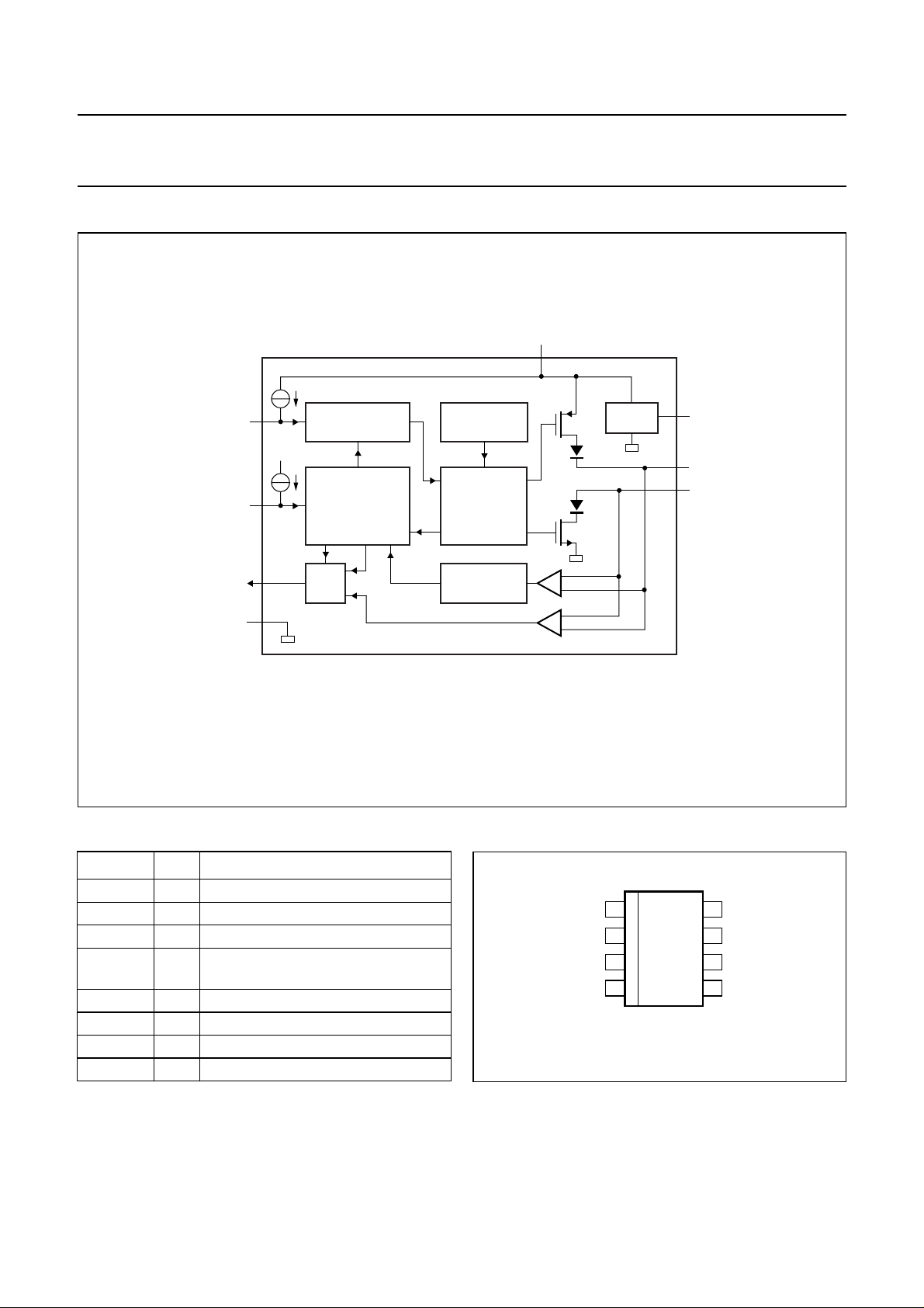
BLOCK DIAGRAM
handbook, full pagewidth
TXD
STB
RXD
GND
1
V
CC
8
4
2
TIME-OUT &
SLOPE
WAKE-UP
MODE CONTROL
MUX
TJA1040
TEMPERATURE
PROTECTION
DRIVER
WAKE-UP
FILTER
Fig.1 Block diagram.
V
CC
3
MGU161
5
SPLIT
7
CANH
6
CANL
V SPLIT
PINNING
SYMBOL PIN DESCRIPTION
TXD 1 transmit data input
GND 2 ground supply
V
CC
3 supply voltage
RXD 4 receive data output; reads out data
from the bus lines
SPLIT 5 common-mode stabilization output
CANL 6 LOW-level CAN bus line
CANH 7 HIGH-level CAN bus line
STB 8 standby mode control input
2003 Oct 14 3
handbook, halfpage
TXD
GND
V
CC
RXD
1
2
3
4
TJA1040T
8
7
6
5
MGU160
Fig.2 Pin configuration.
STB
CANH
CANL
SPLIT
Page 4

Philips Semiconductors Product specification
High speed CAN transceiver TJA1040
FUNCTIONAL DESCRIPTION
Operating modes
The TJA1040 provides two modes of operation which are
selectablevia pin STB.See Table 1for adescriptionof the
modes of operation.
Table 1 Operating modes
MODE
PIN
STB
LOW HIGH
PIN RXD
normal LOW bus dominant bus recessive
standby HIGH wake-uprequest
detected
no wake-up
request detected
NORMAL MODE
In thismode thetransceiver is ableto transmitand receive
data via the bus lines CANH andCANL. See Fig.1 for the
block diagram. The differential receiver converts the
analog data on the bus lines into digital data which is
output to pin RXD viathe multiplexer (MUX). The slope of
the output signals on the bus lines is fixed and optimized
in a way that lowest ElectroMagnetic Emission (EME) is
guaranteed.
STANDBY MODE
In this modethe transmitter and receiver are switched off,
and thelow-power differentialreceiver will monitorthe bus
lines. A HIGH level on pin STB activates this low-power
receiver and the wake-up filter, and after t
the state of
BUS
the CAN bus is reflected on pin RXD.
The supply current on VCC is reduced to a minimum in
such a way that ElectroMagnetic Immunity (EMI) is
guaranteed and a wake-up event on the bus lines will be
recognized.
In this mode the bus lines are terminated to ground to
reduce the supply current (ICC) to a minimum. A diode is
added inseries withthe high-side driverof RXDto prevent
areverse currentfrom RXDto VCCinthe unpoweredstate.
In normal mode this diode is bypassed. This diode is not
bypassed instandby modeto reducecurrent consumption.
Split circuit
Pin SPLIT providesa DC stabilizedvoltage of 0.5VCC.Itis
turnedon onlyinnormal mode.Instandby modepin SPLIT
is floating. The V
circuit can be used to stabilize the
SPLIT
recessivecommon-mode voltagebyconnecting pin SPLIT
tothe centretap ofthe splittermination (seeFig.4). Incase
of arecessive bus voltage<0.5VCCdue tothe presence of
an unsupplied transceiverin the network witha significant
leakage current from the bus lines to ground, the split
circuit will stabilize this recessive voltage to 0.5VCC. So a
start of transmission does not cause a step in the
common-mode signal which would lead to poor
ElectroMagnetic Emission (EME) behaviour.
Wake-up
In the standby mode the bus lines are monitored via a
low-power differential comparator. Once the low-power
differential comparator has detecteda dominant bus level
for more than t
, pin RXD will become LOW.
BUS
Over-temperature detection
The outputdrivers areprotected againstover-temperature
conditions. If the virtual junction temperature exceeds the
shutdownjunction temperatureT
,the outputdriverswill
j(sd)
be disableduntil the virtualjunction temperature becomes
lower than T
and TXD becomes recessive again.
j(sd)
By including the TXD condition, the occurrence of output
driver oscillation due to temperature drifts is avoided.
TXD dominant time-out function
A ‘TXD dominant time-out’ timer circuit prevents the bus
lines from being driven to a permanent dominant state
(blocking all network communication) if pin TXD is forced
permanently LOW by a hardware and/or software
application failure. The timer is triggered by a negative
edge on pin TXD.
If the duration of the LOW level on pin TXD exceeds the
internal timer value (t
), the transmitter is disabled,
dom
driving the bus lines into a recessive state. The timer is
reset by a positive edge on pin TXD. The TXD dominant
time-out timet
defines theminimum possible bitrate of
dom
40 kBaud.
Fail-safe features
Pin TXD providesa pull-uptowards VCCin orderto forcea
recessive level in case pin TXD is unsupplied.
Pin STB provides a pull-up towards VCC in order to force
the transceiver into standby mode in case pin STB is
unsupplied.
In the event that the VCC is lost, pins TXD, STB and RXD
will become floating to prevent reverse supplying
conditions via these pins.
2003 Oct 14 4
Page 5

Philips Semiconductors Product specification
High speed CAN transceiver TJA1040
LIMITING VALUES
In accordance with the Absolute Maximum Rating System (IEC 60134).
SYMBOL PARAMETER CONDITIONS MIN. MAX. UNIT
V
CC
V
TXD
V
RXD
V
STB
V
CANH
V
CANL
V
SPLIT
V
trt
V
esd
T
vj
T
stg
supply voltage no time limit −0.3 +6 V
operating range 4.75 5.25 V
DC voltage on pin TXD −0.3 VCC+ 0.3 V
DC voltage on pin RXD −0.3 VCC+ 0.3 V
DC voltage on pins STB −0.3 VCC+ 0.3 V
DC voltage on pin CANH 0 < VCC< 5.25 V; no time limit −27 +40 V
DC voltage on pin CANL 0 < VCC< 5.25 V; no time limit −27 +40 V
DC voltage on pin SPLIT 0 < VCC< 5.25 V; no time limit −27 +40 V
transient voltages on pins CANH,
according to ISO 7637; see Fig.5 −200 +200 V
CANL and SPLIT
electrostatic discharge voltage Human Body Model (HBM); note 1
pins CANH and CANL
−6+6kV
and SPLIT
all other pins −4+4kV
Machine Model (MM); note 2 −200 +200 V
virtual junction temperature note 3 −40 +150 °C
storage temperature −55 +150 °C
Notes
1. Equivalent to discharging a 100 pF capacitor via a 1.5 kΩ series resistor.
2. Equivalent to discharging a 200 pF capacitor via a 0.75 µH series inductor and a 10 Ω series resistor.
3. Junction temperature in accordance with IEC 60747-1. An alternative definition of Tvjis: Tvj=T
where R
th(vj-amb)
combinations of power dissipation (P) and ambient temperature (T
is a fixed value to be used for the calculating of Tvj. The rating for Tvj limits the allowable
).
amb
amb
+P×R
THERMAL CHARACTERISTICS
In accordance with IEC 60747-1.
SYMBOL PARAMETER CONDITIONS VALUE UNIT
R
th(vj-a)
thermal resistance from virtual junction
in free air 145 K/W
to ambient in SO8 package
R
th(vj-s)
thermal resistance from virtual junction
in free air 50 K/W
to substrate of bare die
QUALITY SPECIFICATION
Quality specification in accordance with
“AEC-Q100”
.
th(vj-amb)
,
2003 Oct 14 5
Page 6

Philips Semiconductors Product specification
High speed CAN transceiver TJA1040
CHARACTERISTICS
VCC= 4.75 to 5.25 V, Tvj= −40 to +150 °C and RL=60Ω unless specified otherwise; all voltages are defined with
respect to ground; positive currents flow into the IC; note 1.
SYMBOL PARAMETER CONDITIONS MIN. TYP. MAX. UNIT
Supply (pin V
I
CC
)
CC
supply current standby mode 5 10 15 µA
normal mode
recessive; V
dominant; V
Transmit data input (pin TXD)
V
IH
V
IL
I
IH
I
IL
C
i
HIGH-level input voltage 2 − VCC+ 0.3 V
LOW-level input voltage −0.3 − +0.8 V
HIGH-level input current V
TXD=VCC
LOW-level input current normal mode; V
input capacitance not tested − 510pF
Standby mode control input (pin STB)
V
IH
V
IL
I
IH
I
IL
HIGH-level input voltage 2 − VCC+ 0.3 V
LOW-level input voltage −0.3 − +0.8 V
HIGH-level input current V
LOW-level input current V
STB=VCC
=0V −1 −4 −10 µA
STB
Receive data output (pin RXD)
V
OH
I
OH
I
OL
HIGH-level output voltage standby mode;
I
= −100 µA
RXD
HIGH-level output current normal mode;
V
RXD=VCC
LOW-level output current V
= 0.4 V 2 6 12 mA
RXD
Common-mode stabilization output (pin SPLIT)
V
O
output voltage normal mode;
−500 µA<IO< +500 µA
I
leakage current standby mode;
L
−22V<V
Bus lines (pins CANH and CANL)
V
O(dom)
dominant output voltage V
TXD
=0V
pin CANH 3 3.6 4.25 V
pin CANL 0.5 1.4 1.75 V
V
O(dom)(m)
V
O(dif)(bus)
matching of dominant output
voltage (VCC-V
CANH-VCANL
differential bus output voltage
(V
CANH
− V
CANL
)
)
V
= 0 V; dominant;
TXD
45 Ω <RL<65Ω
V
TXD=VCC
no load
TXD=VCC
TXD
TXD
− 0.4 V
< +35 V
SPLIT
; recessive;
2.5 5 10 mA
=0V305070mA
−50 +5µA
=0V −100 −200 −300 µA
− 0 −µA
VCC− 1.1 VCC− 0.7 VCC− 0.4 V
−0.1 −0.4 −1mA
0.3V
CC
0.5V
CC
0.7V
CC
V
− 05µA
−100 0 +150 mV
1.5 − 3.0 V
−50 − +50 mV
2003 Oct 14 6
Page 7

Philips Semiconductors Product specification
High speed CAN transceiver TJA1040
SYMBOL PARAMETER CONDITIONS MIN. TYP. MAX. UNIT
V
O(reces)
I
O(sc)
I
O(reces)
V
dif(th)
V
hys(dif)
I
LI
R
i(cm)
R
i(cm)(m)
R
i(dif)
C
i(cm)
C
i(dif)
Timing characteristics; see Fig.8
t
d(TXD-BUSon)
t
d(TXD-BUSoff)
t
d(BUSon-RXD)
t
d(BUSoff-RXD)
t
PD(TXD-RXD)
t
dom(TXD)
t
BUS
t
d(stb-norm)
Thermal shutdown
T
j(sd)
Note
1. All parametersare guaranteedover thevirtualjunction temperaturerange bydesign, but only100% testedat 125 °C
ambient temperature for dies on wafer level, and in addition to this 100% tested at 25 °C ambient temperature for
cased products; unless specified otherwise. For bare dies, all parameters are only guaranteedwith the backside of
the die connected to ground.
recessive output voltage normal mode;V
TXD=VCC
;
2 0.5V
3V
CC
no load
standby mode; no load −0.1 0 +0.1 V
short-circuit output current V
recessive output current −27V<V
differential receiver threshold
voltage
=0V
TXD
pin CANH; V
pin CANL; V
−12V<V
−12V<V
=0V −40 −70 −95 mA
CANH
= 40 V 40 70 100 mA
CANL
< +32 V −2.5 − +2.5 mA
CAN
< +12 V;
CANL
< +12 V
CANH
normal mode(see Fig.6) 0.5 0.7 0.9 V
standby mode 0.4 0.7 1.15 V
differential receiver hysteresis
voltage
input leakage current VCC=0V;
common-mode input
normal mode;
−12V<V
−12V<V
CANL
CANH
< +12 V;
< +12 V
50 70 100 mV
−50 +5µA
V
CANH=VCANL
=5V
standby or normal mode 15 25 35 kΩ
resistance
common-mode input
V
CANH=VCANL
−3 0 +3 %
resistance matching
differential input resistance standby or normal mode 25 50 75 kΩ
common-mode input
V
TXD=VCC
; not tested −−20 pF
capacitance
differential input capacitance V
TXD=VCC
; not tested −−10 pF
delay TXD to bus active normal mode 25 70 110 ns
delay TXD to bus inactive 10 50 95 ns
delay bus active to RXD 15 65 115 ns
delay bus inactive to RXD 35 100 160 ns
propagation delay TXDto RXD V
TXD dominant time-out V
dominant time for wake-up via
=0V 40 − 255 ns
STB
= 0 V 300 600 1000 µs
TXD
standby mode 0.75 1.75 5 µs
bus
delay standby mode to normal
normal mode 5 7.5 10 µs
mode
shutdown junction temperature 155 165 180 °C
2003 Oct 14 7
Page 8

Philips Semiconductors Product specification
High speed CAN transceiver TJA1040
APPLICATION AND TEST INFORMATION
handbook, full pagewidth
BAT
More application information isavailable in aseparateapplication note.
5 V
CANH
SPLIT
CANL
Fig.3 Typical application for 5 V microcontroller.
7
TJA1040
5
6
V
CC
STB
3
8 Port x
RXD
4
TXD
1
2
V
CC
MICROCONTROLLER
RXD
TXD
MGU164
V
handbook, full pagewidth
CC
TJA1040
V
= 0.5V
SPLIT
in normal mode;
otherwise floating
CC
R
R
GND
Fig.4 Stabilization circuitry and application.
2003 Oct 14 8
CANH
60 Ω
SPLIT
60 Ω
CANL
MGU162
Page 9

Philips Semiconductors Product specification
High speed CAN transceiver TJA1040
+
handbook, full pagewidth
5 V
500 kHz
TXD
RXD
15 pF
100 nF47 µF
1
TJA1040
4
V
CC
3
82
GND STB
7
6
5
CANH
CANL
SPLIT
MGW336
1 nF
1 nF
TRANSIENT
GENERATOR
The waveforms of the applied transients will be in accordance with ISO 7637 part 1, test pulses 1, 2, 3a, 3b, 5, 6 and 7.
Fig.5 Test circuit for automotive transients.
handbook, full pagewidth
V
RXD
hysteresis
0.5 0.9
V
i(dif)(bus)
MGS378
HIGH
LOW
(V)
Fig.6 Hysteresis of the receiver.
2003 Oct 14 9
Page 10

Philips Semiconductors Product specification
High speed CAN transceiver TJA1040
+
handbook, full pagewidth
5 V
TXD
SPLIT
RXD
15 pF
100 nF47 µF
1
5
TJA1040
4
V
CC
3
82
GND STB
7
6
CANH
CANL
MGW335
R
L
60 Ω
C
L
100 pF
handbook, full pagewidth
TXD
CANH
CANL
V
i(dif)(bus)
RXD
t
d(TXD-BUSon)
t
d(BUSon-RXD)
Fig.7 Test circuit for timing characteristics.
0.9 V
(1)
0.5 V
0.7V
t
d(TXD-BUSoff)
)
t
PD(TXD-RXD
0.3V
)
CC
t
PD(TXD-RXD
HIGH
LOW
dominant
(BUS on)
recessive
(BUS off)
HIGH
CC
LOW
t
d(BUSoff-RXD)
MGS377
(1) V
i(dif)(bus)=VCANH
− V
CANL
.
Fig.8 Timing diagram.
2003 Oct 14 10
Page 11

Philips Semiconductors Product specification
High speed CAN transceiver TJA1040
BONDING PAD LOCATIONS
COORDINATES
(1)
SYMBOL PAD
xy
TXD 1 119.5 114.5
GND 2 648.5 85
V
CC
3 1214.25 114.5
RXD 4 1635.25 114.5
SPLIT 5 1516.5 1275
CANL 6 990.5 1273.75
CANH 7 530.25 1273.75
STB 8 113.75 1246
Note
1. All x/y coordinatesrepresent the positionof the centre
of each pad (in µm) with respect to the left hand
bottom corner of the top aluminium layer (see Fig.9).
8
handbook, halfpage
x
0
0
y
The backside of the bare die must be connected to ground.
76 5
TJA1040U
1
234
Fig.9 Bonding pad locations.
test pad 1
test pad 2
MBL584
2003 Oct 14 11
Page 12

Philips Semiconductors Product specification
High speed CAN transceiver TJA1040
PACKAGE OUTLINE
SO8: plastic small outline package; 8 leads; body width 3.9 mm
SOT96-1
y
Z
8
pin 1 index
1
D
c
5
A
2
A
1
4
e
w M
b
p
E
H
E
detail X
A
X
v M
A
Q
(A )
L
p
L
A
3
θ
0 2.5 5 mm
scale
DIMENSIONS (inch dimensions are derived from the original mm dimensions)
mm
OUTLINE
VERSION
SOT96-1
A
max.
1.75
0.069
A1A2A
0.25
1.45
0.10
1.25
0.010
0.057
0.004
0.049
IEC JEDEC JEITA
076E03 MS-012
0.25
0.01
b
3
p
0.49
0.25
0.36
0.19
0.019
0.0100
0.014
0.0075
UNIT
inches
Notes
1. Plastic or metal protrusions of 0.15 mm (0.006 inch) maximum per side are not included.
2. Plastic or metal protrusions of 0.25 mm (0.01 inch) maximum per side are not included.
(1)E(2)
cD
5.0
4.8
0.20
0.19
REFERENCES
eHELLpQZywv θ
4.0
1.27
3.8
0.16
0.05
0.15
2003 Oct 14 12
6.2
5.8
0.244
0.228
1.05
1.0
0.4
0.039
0.016
0.7
0.6
0.028
0.024
0.25 0.10.25
0.010.010.041 0.004
EUROPEAN
PROJECTION
(1)
0.7
0.3
0.028
0.012
ISSUE DATE
99-12-27
03-02-18
o
8
o
0
Page 13

Philips Semiconductors Product specification
High speed CAN transceiver TJA1040
SOLDERING
Introduction to soldering surface mount packages
Thistext givesa verybriefinsight toa complextechnology.
A more in-depth account of soldering ICs can be found in
our
“Data Handbook IC26; Integrated Circuit Packages”
(document order number 9398 652 90011).
There is no soldering method that is ideal for all surface
mount IC packages. Wave soldering can still be used for
certainsurface mountICs, butitis notsuitable forfinepitch
SMDs. In these situations reflow soldering is
recommended.
Reflow soldering
Reflow soldering requires solder paste (a suspension of
fine solder particles, flux and binding agent) to be applied
tothe printed-circuitboard byscreen printing,stencilling or
pressure-syringe dispensing before package placement.
Driven by legislation and environmental forces the
worldwide use of lead-free solder pastes is increasing.
Several methods exist for reflowing; for example,
convection or convection/infrared heating in a conveyor
type oven. Throughput times (preheating, soldering and
cooling) vary between 100 and 200 seconds depending
on heating method.
Typical reflow peak temperatures range from
215 to 270 °C depending on solder paste material. The
top-surface temperature of the packages should
preferably be kept:
• below 220 °C (SnPbprocess) or below 245 °C (Pb-free
process)
– for all BGA and SSOP-T packages
– for packages with a thickness ≥ 2.5 mm
– for packages with a thickness < 2.5 mm and a
volume ≥ 350 mm3 so called thick/large packages.
• below 235 °C (SnPbprocess) or below 260 °C (Pb-free
process) for packages witha thickness < 2.5 mm and a
volume < 350 mm3 so called small/thin packages.
Moisture sensitivity precautions, as indicated on packing,
must be respected at all times.
Wave soldering
To overcome these problems the double-wave soldering
method was specifically developed.
If wave soldering isusedthe following conditions must be
observed for optimal results:
• Use a double-wave soldering method comprising a
turbulent wavewith high upward pressurefollowed by a
smooth laminar wave.
• For packages with leads on two sides and a pitch (e):
– larger than or equal to 1.27 mm, the footprint
longitudinal axis is preferred to be parallel to the
transport direction of the printed-circuit board;
– smaller than 1.27 mm, the footprint longitudinal axis
must be parallel to the transport direction of the
printed-circuit board.
The footprint must incorporate solder thieves at the
downstream end.
• Forpackages withleads onfoursides, thefootprint must
be placedat a 45° angle tothe transport direction ofthe
printed-circuit board. The footprint must incorporate
solder thieves downstream and at the side corners.
During placementand beforesoldering, the packagemust
be fixed with a droplet of adhesive. The adhesive can be
applied by screen printing, pin transfer or syringe
dispensing. The package can be soldered after the
adhesive is cured.
Typical dwell time of the leads in the wave ranges from
3 to 4 seconds at 250 °C or 265 °C, depending on solder
material applied, SnPb or Pb-free respectively.
A mildly-activated flux will eliminate the need for removal
of corrosive residues in most applications.
Manual soldering
Fix the component by first soldering two
diagonally-opposite end leads.Use a low voltage(24 V or
less) soldering iron applied to the flat part of the lead.
Contact time must be limited to 10 seconds at up to
300 °C.
When using a dedicated tool, all other leads can be
soldered in one operation within 2 to 5 seconds between
270 and 320 °C.
Conventional single wave soldering is not recommended
forsurface mountdevices (SMDs)orprinted-circuit boards
with a high component density, as solder bridging and
non-wetting can present major problems.
2003 Oct 14 13
Page 14

Philips Semiconductors Product specification
High speed CAN transceiver TJA1040
Suitability of surface mount IC packages for wave and reflow soldering methods
PACKAGE
BGA, LBGA, LFBGA, SQFP, SSOP-T
(1)
(3)
, TFBGA, VFBGA not suitable suitable
DHVQFN, HBCC, HBGA, HLQFP, HSQFP, HSOP, HTQFP,
not suitable
SOLDERING METHOD
WAVE REFLOW
(4)
suitable
(2)
HTSSOP, HVQFN, HVSON, SMS
(5)
PLCC
LQFP, QFP, TQFP not recommended
SSOP, TSSOP, VSO, VSSOP not recommended
PMFP
, SO, SOJ suitable suitable
(5)(6)
suitable
(7)
suitable
(8)
not suitable not suitable
Notes
1. Formore detailedinformation onthe BGApackages refertothe
“(LF)BGAApplication Note
”(AN01026); ordera copy
from your Philips Semiconductors sales office.
2. All surface mount (SMD) packages are moisture sensitive. Depending upon the moisture content, the maximum
temperature (with respect to time) and body size of the package, there is a risk that internal or external package
cracks may occur due to vaporizationof the moisture in them (the so called popcorn effect). For details,refer to the
Drypack information in the
“Data Handbook IC26; Integrated Circuit Packages; Section: Packing Methods”
.
3. These transparent plastic packages are extremely sensitive to reflow soldering conditions and must on no account
be processedthrough more thanone soldering cycleor subjected toinfrared reflow solderingwith peak temperature
exceeding 217 °C ± 10 °C measured in the atmosphere of the reflow oven. The package body peak temperature
must be kept as low as possible.
4. These packages are not suitable for wave soldering. On versions with the heatsink on the bottom side, the solder
cannot penetrate between the printed-circuit boardandthe heatsink. On versions with the heatsink on the top side,
the solder might be deposited on the heatsink surface.
5. If wave soldering is considered, then the package must be placed at a 45° angle to the solder wave direction.
The package footprint must incorporate solder thieves downstream and at the side corners.
6. Wave solderingis suitable forLQFP, TQFP andQFP packages witha pitch (e) largerthan 0.8 mm; itis definitely not
suitable for packages with a pitch (e) equal to or smaller than 0.65 mm.
7. Wave soldering is suitable for SSOP, TSSOP, VSO and VSSOP packages with a pitch (e) equal to or larger than
0.65 mm; it is definitely not suitable for packages with a pitch (e) equal to or smaller than 0.5 mm.
8. Hot bar or manual soldering is suitable for PMFP packages.
REVISION HISTORY
REV DATE CPCN DESCRIPTION
6 20031014 200307014 Product specification (9397 750 11837)
Modification:
• Change ‘V
= 0.5 V’ in standby mode into ‘V
th(dif)
• Add Chapter REVISION HISTORY
5 20030219 − Product specification (9397 750 10887)
2003 Oct 14 14
dif(th)
= 0.4 V’
Page 15

Philips Semiconductors Product specification
High speed CAN transceiver TJA1040
DATA SHEET STATUS
LEVEL
DATA SHEET
STATUS
(1)
PRODUCT
STATUS
(2)(3)
DEFINITION
I Objective data Development This data sheet contains data from the objective specification for product
development. Philips Semiconductors reserves the right to change the
specification in any manner without notice.
II Preliminary data Qualification This data sheet contains data from the preliminary specification.
Supplementary data will be published at a later date. Philips
Semiconductors reserves the right to change the specification without
notice, in order to improve the design and supply the best possible
product.
III Product data Production This data sheet contains data from the product specification. Philips
Semiconductors reserves the right to make changes at any time in order
to improve the design, manufacturing and supply. Relevant changes will
be communicated via a Customer Product/Process Change Notification
(CPCN).
Notes
1. Please consult the most recently issued data sheet before initiating or completing a design.
2. The product status of the device(s) described in this data sheet may have changed since this data sheet was
published. The latest information is available on the Internet at URL http://www.semiconductors.philips.com.
3. For datasheets describingmultipletype numbers,the highest-level productstatus determines thedata sheetstatus.
DEFINITIONS
DISCLAIMERS
Short-form specification The data in a short-form
specification is extracted from a full data sheet with the
same type number and title. For detailed information see
the relevant data sheet or data handbook.
Limiting valuesdefinition Limitingvalues givenare in
accordance with the Absolute Maximum Rating System
(IEC 60134). Stress above one or more of the limiting
values may cause permanent damage to the device.
These are stress ratings only and operation of the device
atthese orat anyother conditionsabovethose givenin the
Characteristics sectionsof the specification isnot implied.
Exposure to limiting values for extended periods may
affect device reliability.
Application information Applications that are
described herein for any of these products are for
illustrative purposes only. Philips Semiconductors make
norepresentation orwarrantythat suchapplications willbe
suitable for the specified use without further testing or
modification.
Life support applications These products are not
designed for use in life support appliances, devices, or
systems where malfunction of these products can
reasonably beexpected toresult inpersonal injury.Philips
Semiconductorscustomers usingorselling theseproducts
for use in such applications do so at their own risk and
agree to fully indemnify Philips Semiconductors for any
damages resulting from such application.
Right to make changes Philips Semiconductors
reserves the right to make changes in the products including circuits, standard cells, and/or software described or contained herein in order to improve design
and/or performance.When theproduct is infull production
(status ‘Production’), relevant changes will be
communicated via a Customer Product/Process Change
Notification (CPCN). Philips Semiconductorsassumes no
responsibility or liability for the use of any of these
products, conveys no licence or title under any patent,
copyright, or mask work right to these products, and
makes no representations or warranties that these
products are free from patent, copyright, or mask work
right infringement, unless otherwise specified.
2003 Oct 14 15
Page 16

Philips Semiconductors Product specification
High speed CAN transceiver TJA1040
Bare die All die are tested and are guaranteed to
comply with all data sheet limits up to the point of wafer
sawing for a period of ninety (90) days from the date of
Philips' delivery. If there are data sheet limits not
guaranteed, these will be separately indicated in the data
sheet. There are no post packing tests performed on
individual die or wafer. Philips Semiconductors has no
control of third party procedures in the sawing, handling,
packing or assembly of the die. Accordingly, Philips
Semiconductors assumes no liability for device
functionality or performance of the die or systems after
third party sawing, handling, packing or assembly of the
die. It is the responsibility of the customer to test and
qualify their application in which the die is used.
2003 Oct 14 16
Page 17

Philips Semiconductors – a w orldwide compan y
Contact information
For additional information please visit http://www.semiconductors.philips.com. Fax: +31 40 27 24825
For sales offices addresses send e-mail to: sales.addresses@www.semiconductors.philips.com.
© Koninklijke Philips Electronics N.V. 2003
All rights are reserved. Reproduction in whole or in part is prohibited without the prior written consent of the copyright owner.
The information presented in this document doesnot formpart of any quotation or contract, isbelieved tobe accurate and reliable and may bechanged
without notice. No liability will be accepted by the publisher for any consequence of its use. Publication thereof does not convey nor imply any license
under patent- or other industrial or intellectual property rights.
Printed in The Netherlands R16/06/pp17 Date of release: 2003 Oct 14 Document order number: 9397750 11837
SCA75
 Loading...