

Page 1

INTEGRATED CIRCUITS
DATA SH EET
TJA1020
LIN transceiver
Product specification
Supersedes data of 2002 Jul 17
2004 Jan 13
Page 2
Philips Semiconductors Product specification
LIN transceiver TJA1020
FEATURES
General
• Baud rate up to 20 Kbaud
• Very low ElectroMagnetic Emission (EME)
• High ElectroMagnetic Immunity (EMI)
• Low slope mode for an even further reduction of EME
• Passive behaviour in unpowered state
• Input levels compatible with 3.3 and 5 V devices
• Integrated termination resistor for Local Interconnect
Network (LIN) slave applications
• Wake-up source recognition (local or remote)
• Supports K-line like functions.
Low power management
• Very low current consumption in sleep mode with local
and remote wake-up.
Protections
• Transmit data (TXD) dominant time-out function
• Bus terminal and battery pin protected against
transients in the automotive environment (ISO7637)
• Bus terminal short-circuit proof to battery and ground
• Thermally protected.
GENERAL DESCRIPTION
The TJA1020 is the interface between the LIN
master/slave protocol controller and the physical bus in a
Local Interconnect Network (LIN). It is primarily intended
forin-vehiclesub-networksusingbaudratesfrom2.4 upto
20 Kbaud.
The transmit data stream of the protocol controller at the
TXD input is converted by the LIN transceiver into a bus
signal with controlled slew rate and wave shaping to
minimize EME. The LIN bus output pin is pulled HIGH via
an internal termination resistor. For a master application
an external resistor in series with a diode should be
connected between pin INH or pin BAT and pin LIN. The
receiver detects the data stream at the LIN bus input pin
and transfers it via pin RXD to the microcontroller.
In normal transceiver operation the TJA1020 can be
switched in the normal slope mode or the low slope mode.
In the low slope mode the TJA1020 lengthens the rise and
fall slopes of the LIN bus signal, thus further reducing the
already very low emission in normal slope mode.
In sleep mode the power consumption of the TJA1020 is
verylow,whereasin failure modes the power consumption
is reduced to a minimum.
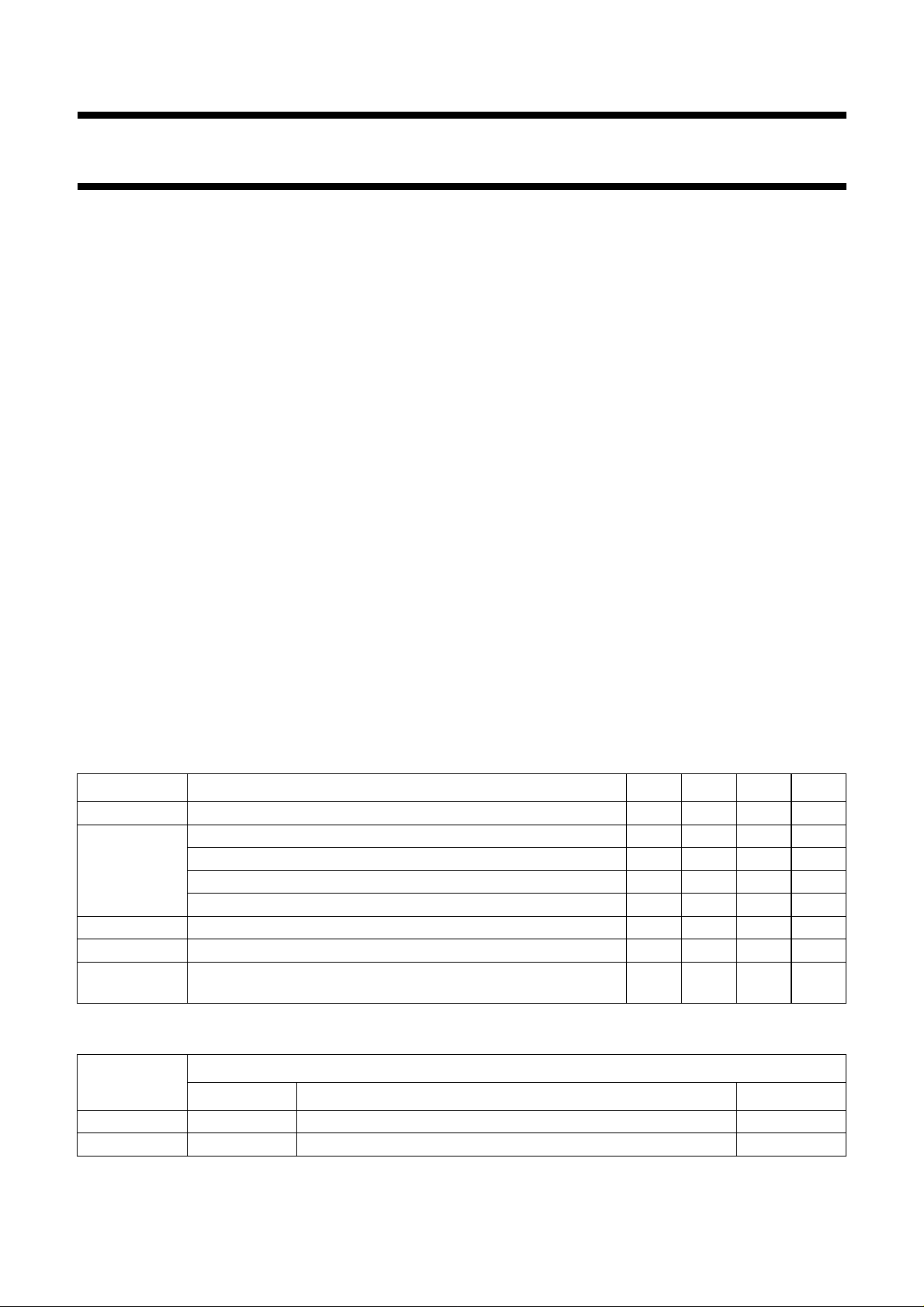
QUICK REFERENCE DATA
SYMBOL PARAMETER MIN. TYP. MAX. UNIT
V
I
BAT
BAT
supply voltage on pin BAT 5 12 27 V
supply current on pin BAT in sleep mode 1 3 8 µA
supply current on pin BAT in standby mode; bus recessive 100 400 1000 µA
supply current on pin BAT in normal slope mode; bus recessive 100 400 1000 µA
supply current on pin BAT in normal slope mode; bus dominant 1 3.5 8.0 mA
V
LIN
T
vj
V
esd(HBM)
DC voltage on pin LIN −27 − +40 V
virtual junction temperature −40 − +150 °C
electrostatic discharge voltage; human body model;
−4 − +4 kV
pins NWAKE, LIN and BAT
ORDERING INFORMATION
TYPE
NUMBER
NAME DESCRIPTION VERSION
PACKAGES
TJA1020T SO8 plastic small outline package; 8 leads; body width 3.9 mm SOT96-1
TJA1020U − bare die; die dimensions 1480 × 1760 × 375 µm −
2004 Jan 13 2
Page 3
Philips Semiconductors Product specification
LIN transceiver TJA1020
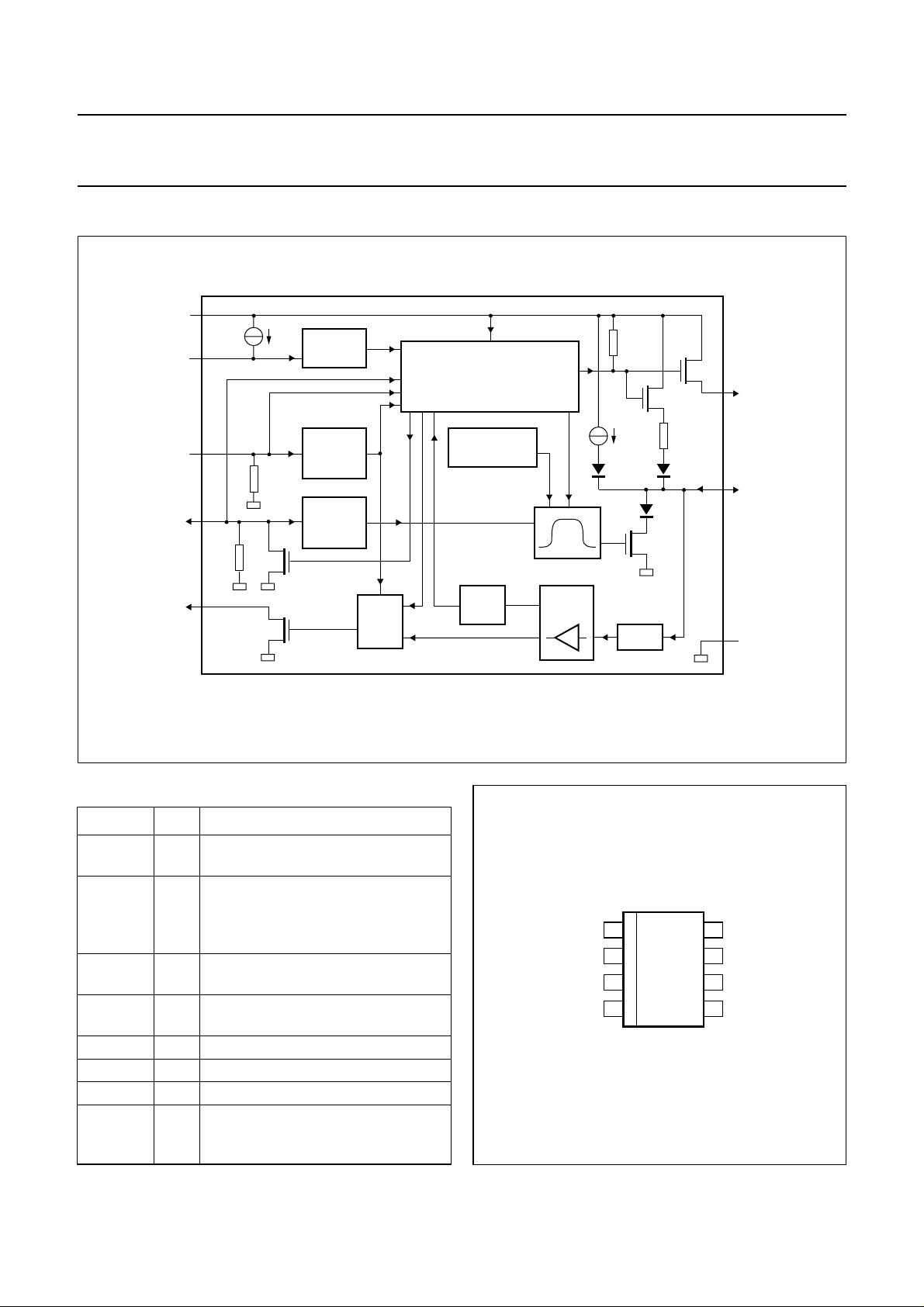
BLOCK DIAGRAM
handbook, full pagewidth
BAT
NWAKE
NSLP
TXD
RXD
7
3
2
4
WAKE-UP
TIMER
SLEEP/
NORMAL
TIMER
TXD
TIME-OUT
TIMER
CONTROL
TEMPERATURE
PROTECTION
8
INH
6
LIN
TJA1020T
1
RXD/
INT
BUS
TIMER
FILTER
MGU241
5
GND
Fig.1 Block diagram.
PINNING
SYMBOL PIN DESCRIPTION
RXD 1 receive data output (open-drain);
active LOW after a wake-up event
NSLP 2 sleep control input (active LOW);
controls inhibit output; resets
wake-up source flag on TXD and
wake-up request on RXD
NWAKE 3 local wake-up input (active LOW);
negative edge triggered
TXD 4 transmit data input; active LOW
output after a local wake-up event
GND 5 ground
LIN 6 LIN bus line input/output
BAT 7 battery supply
INH 8 battery related inhibit output for con-
trolling an external voltage regulator;
active HIGH after a wake-up event
2004 Jan 13 3
handbook, halfpage
RXD
1
NSLP
2
NWAKE
TXD
3
4
TJA1020T
MGU242
Fig.2 Pinning diagram.
8
INH
7
BAT
LIN
6
GND
5
Page 4
Philips Semiconductors Product specification
LIN transceiver TJA1020
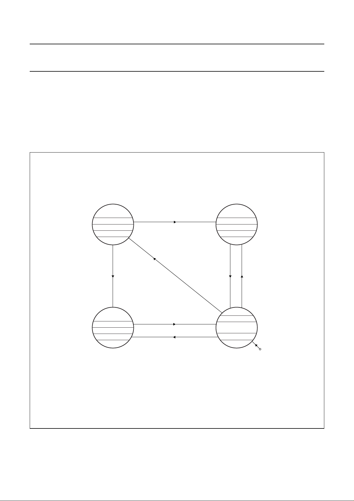
FUNCTIONAL DESCRIPTION
The TJA1020 is the interface between the LIN master/slave protocol controller and the physical bus in a Local
Interconnect Network (LIN). The LIN transceiver is optimized for the maximum specified LIN transmission speed of
20 Kbaud providing optimum EMC performance due to wave shaping of the LIN output.
Operating modes
The TJA1020 provides two modes of normal operation, one intermediate mode and one very low power mode. Figure 3
shows the state diagram.
handbook, full pagewidth
t
(NSLP = 1; after 0−>1)
while TXD = 0
STANDBY
INH = HIGH
TERM. = 30 kΩ
RXD = LOW
> t
gotonorm
SLOPE MODE
INH = HIGH
TERM. = 30 kΩ
RXD = LINDATA
trx OFF
LOW
trx ON
t
(NSLP = 1; after 0−>1)
(t
(NWAKE = 0; after 1−>0)
t
(NSLP = 0; after 1−>0)
t
(NSLP = 1; after 0−>1)
while TXD = 1
t
(LIN = 0; after 1−>0)
or
while TXD = 1
while TXD = 0
> t
gotonorm
> t
NWAKE
> t
)
BUS
t
(NSLP = 0; after 1−>0)
> t
gotosleep
while TXD = 1
> t
gotosleep
> t
gotonorm
NORMAL
SLOPE MODE
INH = HIGH
TERM. = 30 kΩ
RXD = LINDATA
trx ON
t
(NSLP = 1; after 0−>1)
SLEEP
INH = FLOATING
TERM. =
HIGH-OHMIC
RXD = FLOATING
trx OFF
while TXD = 1
switching on BAT
MGU243
> t
gotonorm
trx: transmitter.
TERM.: slave termination resistor, connected between pins LIN and BAT.
Fig.3 State diagram.
2004 Jan 13 4
Page 5

Philips Semiconductors Product specification
LIN transceiver TJA1020
Table 1 Operating modes
MODE NSLP TXD (OUTPUT) RXD INH TRANSMITTER REMARKS
Sleep 0 weak pull-down floating floating off no wake-up request detected
Standby
Normal
slope
mode
Low slope
mode
(1)
0 weak pull-down if
LOW; note 3 HIGH off wake-up request detected; in
remote wake-up;
strong pull-down if
local wake-up;
note 2
1 weak pull-down HIGH:
recessivestate
LOW:
dominant state
1 weak pull-down HIGH:
recessivestate
LOW:
dominant state
this mode the microcontroller
can read the wake-up source:
remote or local wake-up
HIGH normal slope
notes 2, 3 and 4
mode
HIGH low slope mode notes 2, 3 and 5
Notes
1. The standby mode isentered automatically upon any local or remote wake-up event duringsleep mode. Pin INH and
the 30 kΩ termination resistor at pin LIN are switched on.
2. The internal wake-up source flag (set if a local wake-up did occur and fed to pin TXD) will be reset when entering
normal slope or low slope mode (NSLP goes HIGH).
3. The wake-up interrupt (on pin RXD) is released when entering normal slope or low slope mode (NSLP goes HIGH).
4. The normal slope mode is entered during a positive edge on NSLP while pin TXD is already set HIGH. In the event
of a short-circuit to ground on pin TXD, the transmitter will be disabled.
5. The low slope mode is entered during the positive edge on NSLP while pin TXD is already pulled LOW.
Sleep mode
This mode is the most power saving mode of the TJA1020
and the default state after power-up (first battery supply).
Despiteitsextremelowcurrentconsumption,theTJA1020
can still be waken up remotely via pin LIN, or waken up
locally via pin NWAKE, or activated directly via pin NSLP.
Filters at the inputs of the receiver (LIN), of pin NWAKE
andofpin NSLP are preventing unwanted wake-up events
due to automotive transients or EMI. All wake-up events
have to be maintained for a certain time period (t
t
NWAKE
and t
gotonorm
).
BUS
,
The sleep mode is initiated by a falling edge on the pin
NSLP while TXD is already set HIGH. After a filter time
continuously driven sleep command (pin NSLP = LOW),
pin INH becomes floating.
The sleep mode can be activated independently from the
actual level on pin LIN or NWAKE. So it is guaranteed that
the lowest power consumption is achievable even in case
of a continuous dominant level on pin LIN or a continuous
LOW on pin NWAKE.
Standby mode
The standby mode is entered automatically whenever a
local or remote wake-up occurs while the TJA1020 is in its
sleep mode. These wake-up events activate pin INH and
enable the slave termination resistor at the pin LIN. As a
result of the HIGH condition on pin INH the voltage
regulator and the microcontroller can be activated.
Thestandby mode is signalledby a LOW levelon pin RXD
which can be used as an interrupt for the microcontroller.
In sleep mode the internal slave termination between
pins LIN and BAT is disabled to minimize the power
dissipation in case pin LIN is short-circuited to ground.
Only a weak pull-up between pins LIN and BAT is present.
2004 Jan 13 5
In the standby mode (pin NSLP is still LOW), the condition
of pin TXD (weak pull-down or strong pull-down) indicates
thewake-up source: weak pull-down for aremotewake-up
request and strong pull-down for a local wake-up request.
Page 6

Philips Semiconductors Product specification
LIN transceiver TJA1020
Settingpin NSLPHIGHduring standby mode results in the
following events:
• An immediate reset of the wake-up source flag; thus
releasing the possible strong pull-down at pin TXD
before the actual mode change (after t
gotonorm
) is
performed
• A change into normal slope mode if the HIGH level on
pin NSLP has been maintained for a certain time period
(t
gotonorm
) while pin TXD is pulled HIGH
• A change into low slope mode if the HIGH level on pin
NSLP has been maintained for a certain time period
(t
gotonorm
) while pin TXD is pulled LOW either
deliberately driven by the microcontroller, or due to a
failure. In the event of a short-circuit to ground or an
open-wireon pin TXD, theLIN output remains recessive
(fail safe)
• A reset of the wake-up request signal on pin RXD if the
HIGH level on pin NSLP has been maintained for a
certain time period (t
gotonorm
).
Normal slope mode
In the normal slope mode the transceiver is able to
transmitandreceivedata via the LIN bus line. The receiver
detects the data stream at the LIN bus input pin and
transfers it via pin RXD to the microcontroller (see Fig.1):
HIGH at a recessive level and LOW at a dominant level on
the bus. The receiver has a supply voltage related
threshold with hysteresis and an integrated filter to
suppress bus line noise. The transmit data stream of the
protocol controller at the TXD input is converted by the
transmitter into a bus signal with controlled slew rate and
wave shaping to minimize EME. The LIN bus output pin is
pulled HIGH via an internal slave termination resistor. For
a master application an external resistor in series with a
diode should be connected between pin INH or BAT on
one side and pin LIN on the other side (see Fig.7).
Being in the sleep or standby mode, the TJA1020 enters
normalslope mode whenever a HIGH levelon pin NSLP is
maintained for a time of at least t
gotonorm
provided its
preceding positive edge is executed while pin TXD is
already set to HIGH.
The TJA1020 switches to sleep mode in case of a LOW
level on pin NSLP, maintainedduring a certain time period
(t
gotosleep
) while pin TXD is already set to HIGH.
Low slope mode
In the low slope mode the transmitter output stage drives
the LIN bus line with lengthened rise and fall slopes. This
will further reduce the already outstanding EME in the
normalslopemode. The low slope mode is perfectly suited
for applications where transmission speed is not critical.
The mode selection is done by the LIN transceiver after a
positive edge on pin NSLP, maintained for a certain time
period (t
gotonorm
). If pin TXD is LOW at that time, the low
slope mode is entered, otherwise the normal mode is
entered. The transition to the low slope mode will be
executedduring an open pin TXD (fail-safe),ashort-circuit
from pin TXD to ground (fail-safe) or an intended LOW
level of pin TXD programmed by the microcontroller. The
transmitter is enabled after a LOW-to-HIGH transition on
pin TXD. In the event of a short-circuit to ground on pin
TXD, the transmitter will be disabled.
Wake-up
There are three ways to wake-up a TJA1020 which is in
sleep mode:
1. Remote wake-up via a dominant bus state
2. Local wake-up via a negative edge at pin NWAKE
3. Mode change (pin NSLP is HIGH) from sleep mode to
normal slope/low slope mode.
Remote and local wake-up
A falling edge at pin NWAKE followed by a LOW level
maintained for a certain time period (t
NWAKE
) results in a
local wake-up. The pin NWAKE provides an internal
pull-up towards pin BAT. In order to prevent EMI issues, it
is recommended to connect an unused pin NWAKE to
pin BAT.
If, during power-up, pin NWAKE is LOW for a certain
period of time (t
) this will also result in a local
NWAKE
wake-up.
A falling edge at pin LIN followed by a LOW level
maintained for a certain time period (t
) and a rising
BUS
edge at pin LINrespectively (see Fig.4) results in a remote
wake-up.
After a local or remote wake-up pin INH is activated (it
goes HIGH) and the internal slave termination resistor is
switched on. The wake-up request is indicated by a LOW
active wake-up request signal on pin RXD to interrupt the
microcontroller.
The only difference between the normal slope mode and
the low slope mode is the transmitter behaviour.
2004 Jan 13 6
Page 7

Philips Semiconductors Product specification
LIN transceiver TJA1020
Wake-up via mode transition
It is also possible to set pin INH HIGH with a mode
transition towards normal slope/low slope mode via
pin NSLP. This is useful for applications with a
continuously powered microcontroller.
Wake-up source recognition
The TJA1020 can distinguish between a local wake-up
request on pin NWAKE and a remote wake-up request via
a dominant bus state. The wake-up source flag is set in
case the wake-up request was a local one. The wake-up
source can be read on pin TXD in the standby mode. If an
external pull-up resistor on pin TXD to the power supply
voltage of the microcontroller has been added a HIGH
level indicates a remote wake-up request (weak pull-down
at pin TXD) and a LOW level indicates a local wake-up
request (strong pull-down at pin TXD; much stronger than
the external pull-up resistor).
The wake-up request flag (signalled on pin RXD) as well
as the wake-up source flag (signalled on pin TXD) are
reset immediately, if the microcontroller sets pin NSLP
HIGH.
TXD dominant time-out function
A ‘TXD Dominant Time-out’ timer circuit prevents the bus
line from being driven to a permanent dominant state
(blocking all network communication) if pin TXD is forced
permanently LOW by a hardware and/or software
application failure. The timer is triggered by a negative
edge on pin TXD. If the duration of the LOW level on
pin TXD exceeds the internal timer value (t
dom
), the
transmitter is disabled, drivingthe bus line into a recessive
state. The timer is reset by a positive edge on pin TXD.
Fail-safe features
Pin TXD provides a pull-down to GND in order to force a
predefined level on input pin TXD in case the pin TXD is
unsupplied.
Pin NSLP provides a pull-down to GND in order to force
the transceiver into sleep mode in case the pin NSLP is
unsupplied.
Pin RXD is set floating in case of lost power supply on pin
BAT.
The current of the transmitter output stage is limited in
order to protect the transmitter against short-circuit to pins
BAT or GND.
A loss of power (pins BAT and GND) has no impact to the
bus line and the microcontroller. There are no reverse
currents from the bus. The LIN transceiver can be
disconnected from the power supply without influencing
the LIN bus.
The output driver at pin LIN is protected against
overtemperature conditions. If the junction temperature
exceeds the shutdown junction temperature T
j(sd)
, the
thermal protection circuit disables the output driver. The
driver is enabled again if the junction temperature has
been decreased below T
and a recessive level is
j(sd)
present at pin TXD.
handbook, full pagewidth
V
LIN
0.4V
BAT
LIN dominant
sleep mode standby mode
LIN recessive
t
BUS
Fig.4 Wake-up behaviour.
2004 Jan 13 7
V
BAT
0.6V
ground
MBL371
BAT
Page 8

Philips Semiconductors Product specification
LIN transceiver TJA1020
LIMITING VALUES
In accordance with the Absolute Maximum Rating System (IEC 60134); all voltages are referenced to pin GND.
SYMBOL PARAMETER CONDITIONS MIN. MAX. UNIT
V
BAT
V
TXD
V
LIN
V
NWAKE
I
NWAKE
V
INH
I
INH
V
trt(LIN)
T
vj
T
stg
V
esd(HBM)
V
esd(MM)
, V
RXD
, V
supply voltage on pin BAT −0.3 +40 V
DC voltage on pins TXD, RXD and NSLP −0.3 +7 V
NSLP
DC voltage on pin LIN −27 +40 V
DC voltage on pin NWAKE −1 +40 V
current on pin NWAKE (only relevant if
V
NWAKE<VGND
− 0.3 V; current will flow into
−15 − mA
pin GND)
DC voltage on pin INH −0.3 V
BAT
output current at pin INH −50 +15 mA
transient voltage on pin LIN (ISO7637) −150 +100 V
virtual junction temperature −40 +150 °C
storage temperature −55 +150 °C
electrostatic discharge voltage; human body
note 1
model
on pins NWAKE, LIN and BAT −4+4 kV
on pins RXD, NSLP, TXD and INH −2+2 kV
electrostatic discharge voltage; machine
note 2 −200 +200 V
model; all pins
+ 0.3 V
Notes
1. Equivalent to discharging a 100 pF capacitor through a 1.5 kΩ resistor.
2. Equivalent to discharging a 200 pF capacitor through a 10 Ω resistor and a 0.75 µH coil. In the event of a discharge
from pin INH to pin BAT: −150V<V
esd(MM)
< +150 V.
THERMAL CHARACTERISTICS
According to IEC60747-1.
SYMBOL PARAMETER CONDITION VALUE UNIT
R
th(j-a)
thermal resistance from junction to ambient in
in free air 145 K/W
SO8 package
R
th(j-s)
thermal resistance from junction to substrate
in free air 50 K/W
bare die
QUALITY SPECIFICATION
Quality specification in accordance with
“AEC - Q100”
.
2004 Jan 13 8
Page 9

Philips Semiconductors Product specification
LIN transceiver TJA1020
CHARACTERISTICS
V
= 5 to 27 V; Tvj= −40 to +150 °C; R
BAT
L(LIN-BAT)
currents flow into the IC; typical values are given at V
SYMBOL PARAMETER CONDITIONS MIN. TYP. MAX. UNIT
Supply
I
BAT
supply current on
pin BAT
Pin TXD
V
IH
V
IL
V
hys
R
TXD
HIGH-level input voltage 2 − 7V
LOW-level input voltage −0.3 − +0.8 V
TXD hysteresis voltage 0.03 − 0.5 V
TXD pull-down resistor V
= 500 Ω; all voltages are defined with respect to ground; positive
= 12 V; unless otherwise specified; notes 1 and 2.
BAT
sleep mode
(V
LIN=VBAT
V
NWAKE=VBAT
V
TXD
;
=0V; V
;
NSLP
=0V)
standby mode; bus
recessive (V
V
LIN=VBAT
V
NWAKE=VBAT
V
TXD
;
=0V; V
INH=VBAT
;
=0V)
NSLP
standby mode; bus
dominant (V
V
= 12 V; V
INH
V
V
V
NWAKE
=0V;
TXD
= 0 V); note 3
NSLP
=12V;
BAT
=12V;
=0V;
LIN
low slope mode; bus
recessive (V
V
LIN=VBAT
V
NWAKE=VBAT
V
TXD
;
=5V; V
INH=VBAT
;
=5V)
NSLP
normal slope mode; bus
recessive (V
V
LIN=VBAT
V
NWAKE=VBAT
V
TXD
;
=5V; V
INH=VBAT
;
=5V)
NSLP
low slope mode; bus
dominant (V
V
=12V;
INH
V
V
V
NWAKE
=0V;
TXD
= 5 V); note 3
NSLP
=12V;
BAT
=12V;
normal slope mode; bus
dominant (V
V
=12V;
INH
V
V
V
=12V;
NWAKE
=0V;
TXD
= 5 V); note 3
NSLP
= 5 V 125 350 800 kΩ
TXD
BAT
=12V;
138µA
100 400 1000 µA
;
300 900 2000 µA
100 400 1000 µA
;
100 400 1000 µA
;
1 3.5 8 mA
1 3.5 8 mA
2004 Jan 13 9
Page 10

Philips Semiconductors Product specification
LIN transceiver TJA1020
SYMBOL PARAMETER CONDITIONS MIN. TYP. MAX. UNIT
I
IL
I
OL
Pin NSLP
V
IH
V
IL
V
hys
R
NSLP
I
IL
Pin RXD (open-drain)
I
OL
I
LH
Pin NWAKE
V
IH
V
IL
I
IL
I
LH
Pin INH
R
sw(INH)
I
LH
Pin LIN
V
o(reces)
V
o(dom)
I
LH
I
IL
LOW-level input current V
LOW-level output current
(local wake-up request)
=0V −50+5µA
TXD
standby mode;
V
V
V
=0V;
NWAKE
LIN=VBAT
= 0.4 V
TXD
;
1.5 3 − mA
HIGH-level input voltage 2 − 7V
LOW-level input voltage −0.3 − +0.8 V
NSLP hysteresis voltage 0.03 − 0.5 V
NSLP pull-down resistor V
LOW-level input current V
LOW-level output current normal slope mode;
HIGH-level leakage
current
HIGH-level input voltage V
LOW-level input voltage −0.3 − V
NWAKE pull-up current V
HIGH-level leakage
current
switch-on resistance
between pins BAT and
INH
HIGH-level leakage
current
LIN recessive output
= 5 V 125 350 800 kΩ
NSLP
=0V −50+5µA
NSLP
1.3 3.5 − mA
V
=0V; V
LIN
normal slope mode;
V
LIN=VBAT
=0V −30 −10 −3 µA
NWAKE
V
V
NWAKE
=27V
BAT
=27V;
standby; low slope or
; V
RXD
RXD
= 0.4 V
=5V
−50+5µA
− 1 − V
BAT
−50+5µA
− 30 50 Ω
normal slope mode;
I
= −15 mA;
INH
V
=12V
BAT
sleep mode;
V
= 27 V; V
INH
V
=5V; I
TXD
=27V
BAT
= 0 mA 0.9V
LIN
−50+5µA
BAT
− V
+ 0.3 V
BAT
− 3.3 V
BAT
BAT
V
voltage
LIN dominant output
voltage
V
V
TXD
TXD
=0V; V
=0V; V
= 7.3 V −−1.2 V
BAT
BAT
= 7.3;
0.6 −− V
RL=1kΩ
V
V
TXD
TXD
=0V; V
=0V;V
=18V −−2.0 V
BAT
BAT
=18V;
0.8 −− V
RL=1kΩ
HIGH-level leakage
V
LIN=VBAT
−10+1µA
current
LIN pull-up current sleep mode; V
V
=0V
NSLP
LIN
=0V;
−2 −5 −10 µA
2004 Jan 13 10
Page 11

Philips Semiconductors Product specification
LIN transceiver TJA1020
SYMBOL PARAMETER CONDITIONS MIN. TYP. MAX. UNIT
R
SLAVE
I
o(sc)
V
th(rx)
V
cntr(rx)
V
thr(hys)
Thermal shutdown
T
j(sd)
AC characteristics
∆t
d(TXD-BUSon/off)
∆t
d(TXD-BUSon/off)
∆t
d(BUSon/off-RXD)
t
f(slope)(dom)
t
r(slope)(rec)
slave termination
resistance to pin BAT
short-circuit output
current
receiver threshold
voltage
receiver centre voltage V
receiver threshold
hysteresis voltage
shutdown junction
temperature
TXD propagation delay
failure
TXD propagation delay
failure
RXD propagation delay
failure
fall time LIN
(100% to 0%)
rise time LIN
(0% to 100%)
standby, low slope or
normal slope mode;
V
=0V; V
LIN
V
LIN=VBAT
V
=0V; t<t
TXD
V
LIN=VBAT
V
=0V; t<t
TXD
V
= 7.3 to 27 V 0.4V
BAT
= 7.3 to 27 V 0.475V
BAT
V
= 7.3 to 27 V 0.145V
BAT
=12V
BAT
=12V;
dom
=27V;
dom
normal slope mode;
CL= 10 nF; RL= 500 Ω;
(see Fig.5)
t
PropTxDom
− t
PropTxRec
low slope mode;
CL= 10 nF; RL= 500 Ω;
(see Fig.5)
t
PropTxDom
− t
PropTxRec
normal slope mode and
low slope mode; CL=0;
RL= ∞; voltage on LIN
externally forced; LIN
slope time <500 ns;
C
= 20 pF;
RXD
R
= 2.4 kΩ; (see
RXD
Fig.5)
t
PropRxDom
− t
PropRxRec
normal slope mode;
CL= 10 nF; RL= 500 Ω;
V
= 12 V; transition
BAT
from recessive to
dominant; note 4 (see
Fig.5)
normal slope mode;
CL= 10 nF; RL= 500 Ω;
V
= 12 V; transition
BAT
from dominant to
recessive; note 5 (see
Fig.5)
20 30 47 kΩ
27 40 60 mA
60 90 125 mA
BAT
− 0.6V
0.5V
BAT
0.16V
BAT
BAT
BAT
BAT
0.525V
0.175V
BAT
BAT
V
V
V
160 175 190 °C
−20+2µs
−50+5µs
−20+2µs
− 16 27 µs
− 16 27 µs
2004 Jan 13 11
Page 12

Philips Semiconductors Product specification
LIN transceiver TJA1020
SYMBOL PARAMETER CONDITIONS MIN. TYP. MAX. UNIT
∆t
slope(norm)
t
f(slope)(norm)(dom)
t
r(slope)(norm)(rec)
∆t
slope(norm)
t
f(slope)(low)(dom)
t
r(slope)(low)(rec)
t
BUS
t
NWAKE
t
gotonorm
t
gotosleep
t
dom
normal slope symmetry normal slope mode;
CL= 10 nF; RL= 500 Ω;
V
=12V;
BAT
normal slope fall time LIN
(100% to 0%)
t
f(slope)(dom)
normal slope mode;
CL= 6.8 nF;RL= 660 Ω;
V
BAT
− t
r(slope)(rec)
= 12 V; transition
from recessive to
dominant; note 4
normal slope rise time
LIN (0% to 100%)
normal slope mode;
CL= 6.8 nF;RL= 660 Ω;
V
= 12 V; transition
BAT
from dominant to
recessive; note 5
normal slope symmetry normal slope mode;
CL= 6.8 nF;RL= 660 Ω;
V
=12V;
BAT
low slope fall time LIN
(100% to 0%)
low slope rise time LIN
(0% to 100%)
dominant time for
t
f(slope)(dom)
low slope mode;
CL= 10 nF; RL= 500 Ω;
V
BAT
low slope mode;
CL= 10 nF; RL= 500 Ω;
V
BAT
sleep mode 30 70 150 µs
− t
r(slope)(rec)
= 12 V; note 4
= 12 V; note 5
wake-up via bus
dominant time for
sleep mode 7 20 50 µs
wake-up via pin NWAKE
time period for mode
change from sleep or
standby mode into
normal/low slope mode
time period for mode
change from normal/low
slope mode into sleep
mode
TXD dominant time out V
= 0 V 6 12 20 ms
TXD
−50+5µs
− 12 22.5 µs
− 12 22.5 µs
−40+4µs
− 30 62 µs
− 30 62 µs
2510µs
2510µs
2004 Jan 13 12
Page 13

Philips Semiconductors Product specification
LIN transceiver TJA1020
Notes
1. All parameters are guaranteed over the virtual junction temperature by design, but only 100% tested at 125 °C
ambient temperature for dies on wafer level and, in addition to this, 100% tested at 25 °C ambient temperature for
cased products, unless otherwise specified.
2. For bare die, all parameters are only guaranteed if the backside of the bare die is connected to ground.
3. If V
is higher than 12 V, the battery current increases due to the internal LIN termination resistor. The minimum
BAT
V
BAT
value of this resistor is 20 kΩ. The maximum current increase is therefore:
I
BAT increase()
=
------------------------------- 20 kΩ
12 V–
t
4. ; see Fig.6.
f(slope)(dom)
t
5. ; see Fig.6.
r(slope)(rec)
t
=
--------------------------------------------------------------------------------
t
VLIN
=
---------------------------------------------------------------------------- -
VLIN
40%=()t
0.55
60%=()t
0.55
VLIN
VLIN
95%=()–
5%=()–
TIMING DIAGRAMS
handbook, full pagewidth
V
LIN
50% 50%TXD
t
PropTxDom
100%
95%
0.5 V
BAT
0%
t
PropRxDom
t
PropTxRec
5%
0.5 V
BAT
t
PropRxRec
t
RXD
50%
Fig.5 Timing diagram for AC characteristics, bus loaded.
2004 Jan 13 13
50%
MGW323
Page 14

Philips Semiconductors Product specification
LIN transceiver TJA1020
handbook, full pagewidth
V
LIN
100%
95%
0%
t
slope(Dom)
40%
5%
60%
t
slope(Rec)
t
MGU433
APPLICATION INFORMATION
handbook, full pagewidth
V
DD
MICROCONTROLLER
GND
RX0
TX0
Px.x
Fig.6 Definition of slope timing.
ECU
BATTERY
+5 V/
+3.3 V
RXD
TXD
NSLP
1
4
2
INH
8
TJA1020T
5
GND
7
BAT
3
6
NWAKE
LIN
LIN BUS
LINE
only for
master node
1 kΩ
(1)
MGU244
More information is available in a separate application note.
(1) C
master
= 1 nF; C
slave
= 220 pF.
Fig.7 Typical application of the TJA1020.
2004 Jan 13 14
Page 15

Philips Semiconductors Product specification
LIN transceiver TJA1020
handbook, full pagewidth
100 nF
R
L
MGT992
C
L
R
RXD
C
RXD
NWAKE
NSLP
TXD
RXD
BAT
INH
TJA1020
LIN
GND
handbook, full pagewidth
5 V
10
kΩ
10
kΩ
5 V
Fig.8 Test circuit for AC characteristics.
10 µF
500 Ω
INH
RXD
TXD
NSLP
BAT
NWAKE
TJA1020
LIN
GND
1 nF
TRANSIENT
GENERATOR
MGT993
The waveforms of the applied transients on pin 6 (LIN) and pin 7 (BAT) are according to ISO7637 part 1, test pulses 1, 2, 3a, 3b, 4, 5, 6 and 7.
Fig.9 Test circuit for automotive transients.
2004 Jan 13 15
Page 16

Philips Semiconductors Product specification
LIN transceiver TJA1020
BONDING PAD LOCATIONS
handbook, full pagewidth
1
2
y
3
4
0
0
8
7
x
6
5A 5B 5C
MGW322
Fig.10 Bonding pad locations.
Table 2 Bonding pad locations (dimensions in µm). All x and y co-ordinates are referenced to the bottom left hand
corner of the top aluminium layer.
CO-ORDINATES
SYMBOL PAD
xy
RXD 1 111 1570
NSLP 2 111 1395
NWAKE 3 165 424
TXD 4 134 134
GND1 5A 1075 90
GND2 5B 1185 90
GND3 5C 1295 90
LIN 6 1318 419
BAT 7 1235 1133
INH 8 1125 1490
2004 Jan 13 16
Page 17

Philips Semiconductors Product specification
LIN transceiver TJA1020
PACKAGE OUTLINE
SO8: plastic small outline package; 8 leads; body width 3.9 mm
D
c
y
Z
8
pin 1 index
1
e
5
A
2
A
4
w
b
p
M
SOT96-1
E
H
E
1
L
detail X
A
X
v
M
A
Q
(A )
L
p
A
3
θ
0 2.5 5 mm
scale
DIMENSIONS (inch dimensions are derived from the original mm dimensions)
mm
OUTLINE
VERSION
SOT96-1
A
A1A2A3b
max.
0.25
1.75
0.10
0.010
0.069
0.004
p
1.45
1.25
0.057
0.049
IEC JEDEC JEITA
076E03 MS-012
0.25
0.01
0.49
0.36
0.019
0.014
0.0100
0.0075
UNIT
inches
Notes
1. Plastic or metal protrusions of 0.15 mm (0.006 inch) maximum per side are not included.
2. Plastic or metal protrusions of 0.25 mm (0.01 inch) maximum per side are not included.
cD
0.25
5.0
0.19
4.8
0.20
0.19
REFERENCES
(1)E(2)
4.0
3.8
0.16
0.15
eHELLpQZywv θ
1.27
0.05
2004 Jan 13 17
6.2
5.8
0.244
0.228
1.05
1.0
0.4
0.039
0.016
0.7
0.6
0.028
0.024
0.25 0.10.25
0.010.010.041 0.004
EUROPEAN
PROJECTION
(1)
0.7
0.3
0.028
0.012
ISSUE DATE
99-12-27
03-02-18
o
8
o
0
Page 18

Philips Semiconductors Product specification
LIN transceiver TJA1020
SOLDERING
Introduction to soldering surface mount packages
Thistextgivesavery brief insight to a complex technology.
A more in-depth account of soldering ICs can be found in
our
“Data Handbook IC26; Integrated Circuit Packages”
(document order number 9398 652 90011).
There is no soldering method that is ideal for all surface
mount IC packages. Wave soldering can still be used for
certainsurfacemountICs,butitisnot suitable for fine pitch
SMDs. In these situations reflow soldering is
recommended.
Reflow soldering
Reflow soldering requires solder paste (a suspension of
fine solder particles, flux and binding agent) to be applied
tothe printed-circuit board by screen printing,stencillingor
pressure-syringe dispensing before package placement.
Driven by legislation and environmental forces the
worldwide use of lead-free solder pastes is increasing.
Several methods exist for reflowing; for example,
convection or convection/infrared heating in a conveyor
type oven. Throughput times (preheating, soldering and
cooling) vary between 100 and 200 seconds depending
on heating method.
Typical reflow peak temperatures range from
215 to 270 °C depending on solder paste material. The
top-surface temperature of the packages should
preferably be kept:
• below 225 °C (SnPb process) or below 245 °C (Pb-free
process)
– for all BGA, HTSSON-T and SSOP-T packages
– for packages with a thickness ≥ 2.5 mm
– for packages with a thickness < 2.5 mm and a
volume ≥ 350 mm3 so called thick/large packages
• below 240 °C (SnPb process) or below 260 °C (Pb-free
process) for packages with a thickness < 2.5 mm and a
volume < 350 mm3 so called small/thin packages.
Moisture sensitivity precautions, as indicated on packing,
must be respected at all times.
Wave soldering
To overcome these problems the double-wave soldering
method was specifically developed.
If wave soldering is used the following conditions must be
observed for optimal results:
• Use a double-wave soldering method comprising a
turbulent wave with high upward pressure followed by a
smooth laminar wave.
• For packages with leads on two sides and a pitch (e):
– larger than or equal to 1.27 mm, the footprint
longitudinal axis is preferred to be parallel to the
transport direction of the printed-circuit board;
– smaller than 1.27 mm, the footprint longitudinal axis
must be parallel to the transport direction of the
printed-circuit board.
The footprint must incorporate solder thieves at the
downstream end.
• Forpackageswithleadsonfoursides,the footprint must
be placed at a 45° angle to the transport direction of the
printed-circuit board. The footprint must incorporate
solder thieves downstream and at the side corners.
During placement and before soldering, the package must
be fixed with a droplet of adhesive. The adhesive can be
applied by screen printing, pin transfer or syringe
dispensing. The package can be soldered after the
adhesive is cured.
Typical dwell time of the leads in the wave ranges from
3 to 4 seconds at 250 °C or 265 °C, depending on solder
material applied, SnPb or Pb-free respectively.
A mildly-activated flux will eliminate the need for removal
of corrosive residues in most applications.
Manual soldering
Fix the component by first soldering two
diagonally-opposite end leads. Use a low voltage (24 V or
less) soldering iron applied to the flat part of the lead.
Contact time must be limited to 10 seconds at up to
300 °C.
When using a dedicated tool, all other leads can be
soldered in one operation within 2 to 5 seconds between
270 and 320 °C.
Conventional single wave soldering is not recommended
forsurfacemountdevices(SMDs)orprinted-circuit boards
with a high component density, as solder bridging and
non-wetting can present major problems.
2004 Jan 13 18
Page 19

Philips Semiconductors Product specification
LIN transceiver TJA1020
Suitability of surface mount IC packages for wave and reflow soldering methods
SOLDERING METHOD
WAVE REFLOW
(2)
BGA, HTSSON..T
PACKAGE
(3)
, LBGA, LFBGA, SQFP, SSOP..T
(1)
(3)
, TFBGA,
not suitable suitable
USON, VFBGA
DHVQFN, HBCC, HBGA, HLQFP, HSO, HSOP, HSQFP, HSSON,
not suitable
(4)
suitable
HTQFP, HTSSOP, HVQFN, HVSON, SMS
(5)
PLCC
LQFP, QFP, TQFP not recommended
SSOP, TSSOP, VSO, VSSOP not recommended
CWQCCN..L
, SO, SOJ suitable suitable
(5)(6)
suitable
(7)
suitable
(8)
, PMFP
(9)
, WQCCN..L
(8)
not suitable not suitable
Notes
1. Formoredetailed information on the BGA packagesrefertothe
“(LF)BGAApplication Note
”(AN01026);order a copy
from your Philips Semiconductors sales office.
2. All surface mount (SMD) packages are moisture sensitive. Depending upon the moisture content, the maximum
temperature (with respect to time) and body size of the package, there is a risk that internal or external package
cracks may occur due to vaporization of the moisture in them (the so called popcorn effect). For details, refer to the
Drypack information in the
“Data Handbook IC26; Integrated Circuit Packages; Section: Packing Methods”
.
3. These transparent plastic packages are extremely sensitive to reflow soldering conditions and must on no account
be processed through more than one soldering cycle or subjected to infrared reflow soldering with peak temperature
exceeding 217 °C ± 10 °C measured in the atmosphere of the reflow oven. The package body peak temperature
must be kept as low as possible.
4. These packages are not suitable for wave soldering. On versions with the heatsink on the bottom side, the solder
cannot penetrate between the printed-circuit board and the heatsink. On versions with the heatsink on the top side,
the solder might be deposited on the heatsink surface.
5. If wave soldering is considered, then the package must be placed at a 45° angle to the solder wave direction.
The package footprint must incorporate solder thieves downstream and at the side corners.
6. Wave soldering is suitable for LQFP, TQFP and QFP packages with a pitch (e) larger than 0.8 mm; it is definitely not
suitable for packages with a pitch (e) equal to or smaller than 0.65 mm.
7. Wave soldering is suitable for SSOP, TSSOP, VSO and VSSOP packages with a pitch (e) equal to or larger than
0.65 mm; it is definitely not suitable for packages with a pitch (e) equal to or smaller than 0.5 mm.
8. Image sensor packages in principle should not be soldered. They are mounted in sockets or delivered pre-mounted
on flex foil. However, the image sensor package can be mounted by the client on a flex foil by using a hot bar
soldering process. The appropriate soldering profile can be provided on request.
9. Hot bar or manual soldering is suitable for PMFP packages.
2004 Jan 13 19
Page 20

Philips Semiconductors Product specification
LIN transceiver TJA1020
DATA SHEET STATUS
LEVEL
DATA SHEET
STATUS
(1)
PRODUCT
STATUS
(2)(3)
DEFINITION
I Objective data Development This data sheet contains data from the objective specification for product
development. Philips Semiconductors reserves the right to change the
specification in any manner without notice.
II Preliminary data Qualification This data sheet contains data from the preliminary specification.
Supplementary data will be published at a later date. Philips
Semiconductors reserves the right to change the specification without
notice, in order to improve the design and supply the best possible
product.
III Product data Production This data sheet contains data from the product specification. Philips
Semiconductors reserves the right to make changes at any time in order
to improve the design, manufacturing and supply. Relevant changes will
be communicated via a Customer Product/Process Change Notification
(CPCN).
Notes
1. Please consult the most recently issued data sheet before initiating or completing a design.
2. The product status of the device(s) described in this data sheet may have changed since this data sheet was
published. The latest information is available on the Internet at URL http://www.semiconductors.philips.com.
3. For data sheets describing multiple type numbers, the highest-level product status determines the data sheet status.
REVISION HISTORY
REV DATE CPCN DESCRIPTION
5 2004 01 13 200312021 Product specification (9397 750 11718)
Modifications:
• Chapter “Features”; ‘Supports K-line like functions’ added
• Figure 1; direction arrow on pin TXD added to indicate an output signal
flow as well as an input signal flow.
• Figure 3; conditions on mode transitions defined more accurately
• Chapter “Thermal characteristics”; R
th(j-s)
added (was tbf)
• Recommendation to connect an unused pin NWAKE to pin BAT
incorporated in order to prevent EMI issues
• Specification of LIN dominant output voltage changed to align with
LIN specification 1.3
• Editorial improvements.
4 20020717 − Product specification (9397 750 10028)
value in free air = 50 K/W
2004 Jan 13 20
Page 21

Philips Semiconductors Product specification
LIN transceiver TJA1020
DEFINITIONS
Short-form specification The data in a short-form
specification is extracted from a full data sheet with the
same type number and title. For detailed information see
the relevant data sheet or data handbook.
Limiting values definition Limiting values given are in
accordance with the Absolute Maximum Rating System
(IEC 60134). Stress above one or more of the limiting
values may cause permanent damage to the device.
These are stress ratings only and operation of the device
attheseor at any other conditions above those given inthe
Characteristics sections of the specification is not implied.
Exposure to limiting values for extended periods may
affect device reliability.
Application information Applications that are
described herein for any of these products are for
illustrative purposes only. Philips Semiconductors make
norepresentationorwarrantythatsuchapplicationswillbe
suitable for the specified use without further testing or
modification.
DISCLAIMERS
Life support applications These products are not
designed for use in life support appliances, devices, or
systems where malfunction of these products can
reasonably be expected toresult in personal injury. Philips
Semiconductorscustomersusingorsellingtheseproducts
for use in such applications do so at their own risk and
agree to fully indemnify Philips Semiconductors for any
damages resulting from such application.
Right to make changes Philips Semiconductors
reserves the right to make changes in the products including circuits, standard cells, and/or software described or contained herein in order to improve design
and/or performance. When the product is in full production
(status ‘Production’), relevant changes will be
communicated via a Customer Product/Process Change
Notification (CPCN). Philips Semiconductors assumes no
responsibility or liability for the use of any of these
products, conveys no licence or title under any patent,
copyright, or mask work right to these products, and
makes no representations or warranties that these
products are free from patent, copyright, or mask work
right infringement, unless otherwise specified.
Bare die All die are tested and are guaranteed to
comply with all data sheet limits up to the point of wafer
sawing for a period of ninety (90) days from the date of
Philips' delivery. If there are data sheet limits not
guaranteed, these will be separately indicated in the data
sheet. There are no post packing tests performed on
individual die or wafer. Philips Semiconductors has no
control of third party procedures in the sawing, handling,
packing or assembly of the die. Accordingly, Philips
Semiconductors assumes no liability for device
functionality or performance of the die or systems after
third party sawing, handling, packing or assembly of the
die. It is the responsibility of the customer to test and
qualify their application in which the die is used.
2004 Jan 13 21
Page 22

Philips Semiconductors – a w orldwide compan y
Contact information
For additional information please visit http://www.semiconductors.philips.com. Fax: +31 40 27 24825
For sales offices addresses send e-mail to: sales.addresses@www.semiconductors.philips.com.
© Koninklijke Philips Electronics N.V. 2004
All rights are reserved. Reproduction in whole or in part is prohibited without the prior written consent of the copyright owner.
The information presented in this document does not form part of any quotation or contract, is believed to be accurate and reliable and may be changed
without notice. No liability will be accepted by the publisher for any consequence of its use. Publication thereof does not convey nor imply any license
under patent- or other industrial or intellectual property rights.
Printed in The Netherlands R16/05/pp22 Date of release: 2004 Jan 13 Document order number: 9397 750 11718
SCA76
 Loading...