

Philips tja1010 DATASHEETS

INTEGRATED CIRCUITS
DATA SH EET
TJA1010
Octal Low Side Driver (OLSD)
Preliminary specification
File under Integrated Circuits, IC18
1998 Feb 09
Philips Semiconductors Preliminary specification
Octal Low Side Driver (OLSD) TJA1010
FEATURES
• Eight independent low side drivers
• Small outline/medium power package for surface
mounting, SO28 (20 + 4 + 4)
• Serial input control by writing to internal shift register
• Overvoltage clamping for each driver
• Each driver protected against short-circuited load
• Undervoltage shutdown
• All logic pins CMOS microcontroller compatible
• Standby mode for minimum current consumption
• Two status outputs indicating short-circuited load and
open load respectively at any driver stage
• Channel selective diagnostic information available by
reading from internal shift register
• Serial output allows cascading of several OLSDs
• Outputs can be used in parallel
• Two-stage thermal protection
• Power-on reset.
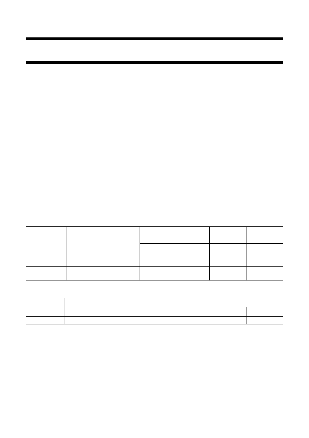
QUICK REFERENCE DATA
GENERAL DESCRIPTION
The TJA1010 is an octal low side driver for relays in
automotive applications.
SYMBOL PARAMETER CONDITIONS MIN. TYP. MAX. UNIT
V
DD
supply voltage operating 5.5 − 25 V
load dump −−50 V
V
o(clamp)
R
o(on)
I
o
drain-to-source clamp voltage Io=20mA 506070V
on resistance Io= 0.2 A −−3Ω
output current continuous at all outputs;
T
=85°C
amb
−−0.2 A
ORDERING INFORMATION
TYPE
NUMBER
NAME DESCRIPTION VERSION
PACKAGE
TJA1010T SO28 plastic small outline package; 28 leads; body width 7.5 mm SOT136-1
1998 Feb 09 2
This text is here in white to force landscape pages to be rotated correctly when browsing through the pdf in the Acrobat reader.This text is here in
_white to force landscape pages to be rotated correctly when browsing through the pdf in the Acrobat reader.This text is here inThis text is here in
white to force landscape pages to be rotated correctly when browsing through the pdf in the Acrobat reader. white to force landscape pages to be ...
1998 Feb 09 3
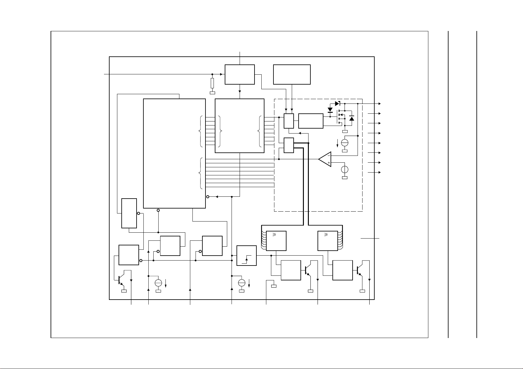
handbook, full pagewidth
STBY
25
serial input
parallel
outputs
8-BIT
SHIFT
REGISTER
parallel
inputs
V
DD
SUPPLY
AND
REFERENCE
master
reset
8-BIT
LATCH
data
inputs
clock
24
UV
power-on
data
outputs
0 V
TEMPERATURE
PROTECTION
CURRENT
LIMITING
TJA1010
1
OUT1
3
OUT2
12
OUT3
14
OUT4
15
OUT5
17
OUT6
26
V
ref
OUT7
28
OUT8
BLOCK DIAGRAM
Octal Low Side Driver (OLSD) TJA1010
Philips Semiconductors Preliminary specification
latch
DQ
clock
&
serial clock
&
parallel
load
serial input
&
DELAY
T
stat
115410
Fig.1 Block diagram.
OL SC
1 1
&
6 to 9
20 to 23
2, 13
16, 27
GND1
to
GND4
&
19
MBH994
18
STATSCSTATOLGNDSIESISCLSO
Philips Semiconductors Preliminary specification
Octal Low Side Driver (OLSD) TJA1010
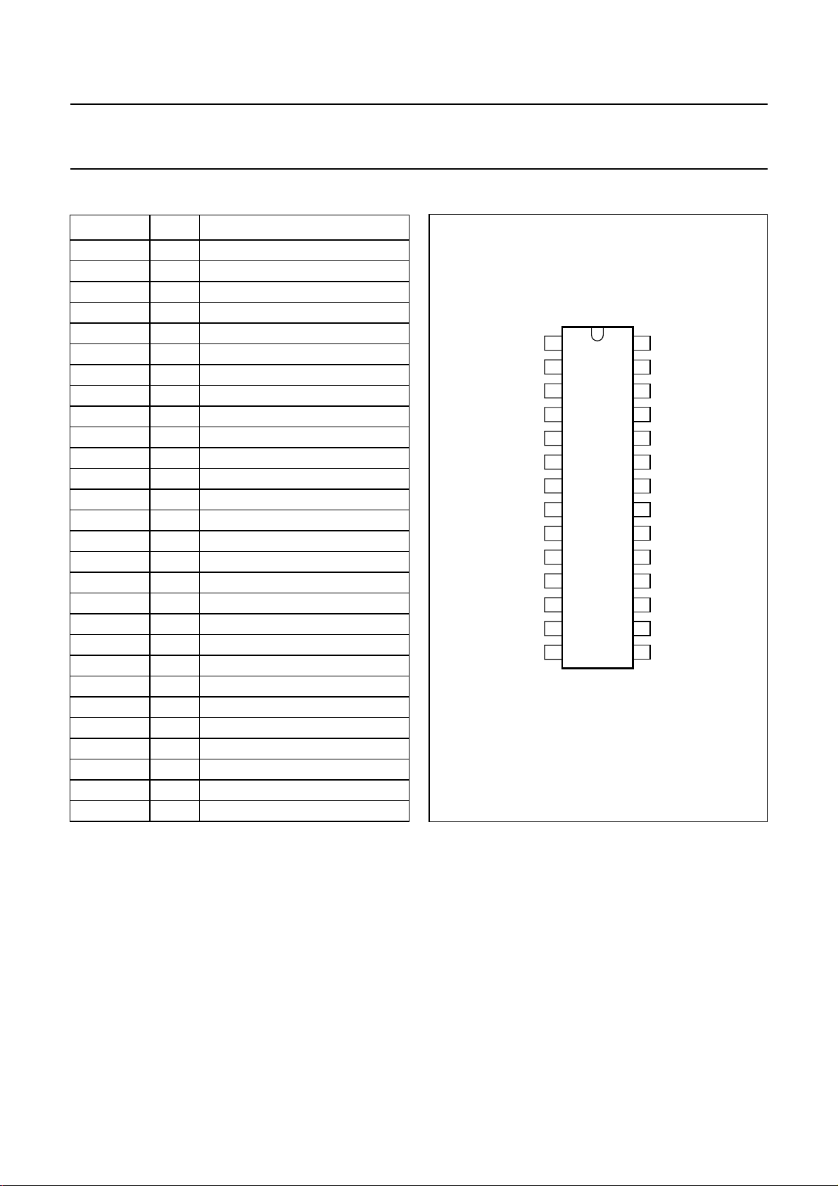
PINNING
SYMBOL PIN DESCRIPTION
OUT1 1 output 1
GND1 2 ground 1
OUT2 3 output 2
SCL 4 serial clock input
SI 5 serial input
GND 6 ground
GND 7 ground
GND 8 ground
GND 9 ground
SO 10 serial output
SIE 11 serial input enable
OUT3 12 output 3
GND2 13 ground 2
OUT4 14 output 4
OUT5 15 output 5
GND3 16 ground 3
OUT6 17 output 6
STATSC 18 status output short-circuited load
STATOL 19 status output open load
GND 20 ground
GND 21 ground
GND 22 ground
GND 23 ground
V
DD
24 supply voltage
STBY 25 standby input
OUT7 26 output 7
GND4 27 ground 4
OUT8 28 output 8
handbook, halfpage
OUT1
1
GND1
2
OUT2
3
SCL
4
SI
5
GND
6
GND
7
TJA1010
8
GND
GND
9
SO
10
SIE
11
OUT3
12
GND2
13
OUT4
MBH990
Fig.2 Pin configuration.
28
27
26
25
24
23
22
21
20
19
18
17
16
1514
OUT8
GND4
OUT7
STBY
V
DD
GND
GND
GND
GND
STATOL
STATSC
OUT6
GND3
OUT5
1998 Feb 09 4

Philips Semiconductors Preliminary specification
Octal Low Side Driver (OLSD) TJA1010
FUNCTIONAL DESCRIPTION (see Figs 1, 3 and 4) This octal low side driver is intended to drive relays in
automotive applications. It is optimized to withstand the
wide temperature and supply voltage range that is typical
for this application area. It consists of 8 protected outputs,
including diagnostic functions, controlled by a serial
interface. These outputs can be used in parallel without the
need for additional components.
Serial control interface
Serial control of the drivers is provided by an 8-bit shift
register with parallel outputs and an 8-bit latch which
controls the DMOS output stages. Using this configuration
the number of pins needed for control of the eight drivers
is reduced to three; Serial Input (SI), Serial CLock (SCL)
and Serial Input Enable (SIE). When pin SIE is LOW, serial
data at pin SI is shifted into the shift register at each
HIGH-to-LOW transition at the SCL pin and serial data is
shifted out at the Serial Output (SO) pin at a LOW-to-HIGH
transition on the SCL pin. The last bit read in before a
LOW-to-HIGH transition at the SIE pin is bit D8. A HIGH
level at the SI pin causes a driver to switch-on. With a
LOW-to-HIGH transition at the SIE pin, parallel output data
in the shift register is written to the 8-bit latch, which
controls the DMOS outputs. When SIE is HIGH, signals at
pins SI, SCL and SO are disabled. For pin SO this results
in a HIGH level because pin SO is an open-collector
output.
Diagnostic interface
The OLSD detects open loads and short-circuited loads at
each driver stage by comparing its output voltages (V
a reference voltage (V
). To allow distinction between
ref
o
) to
short-circuit and open load conditions, a short-circuit is
detected for Vo>V
detected for Vo<V
in the on-state, while an open load is
ref
in the off-state of a driver stage.
ref
In both cases the corresponding status pin is set to a LOW
level and the respective bit in the shift register is inverted
on a HIGH-to-LOW transition of SIE.
By writing a following byte into the shift register, its actual
contents (the control byte eventually modified by errors)
can be read out via pin SO. Comparing this byte with the
original control byte previously written, faults can be
localized and identified (e.g. open load at driver stage
number 5).
Protection of DMOS outputs
Each driver contains a DMOS power FET. The drivers are
protected against overvoltage, short-circuit and
overtemperature conditions.
An overvoltage clamp circuit at each driver causes the
respective DMOS power FET to turn partially on, if its
drain-to-source voltage level exceeds the clamp level
[V
]. Consequently each driver can withstand
o(clamp)
voltage peaks caused by turning off inductive loads, such
as relays coils without freewheel diodes. It should be noted
that if outputs are used in parallel the amount of inductive
energy which can be handled will not increase but will
remain equal to that of a single output.
Each driver is protected against a short-circuited load by
current limiting. In the event of a short-circuited load at a
driver stage, the current will be limited and the HIGH level
of its drain-to-source voltage will force the comparator
output to go HIGH. This in turn will set the STATSC pin to
a LOW level.
A two-stage temperature protection circuit is included to
protect the device against overheating caused by high
dissipation in the output transistors.
When the temperature exceeds the overtemperature
threshold level, it will switch-off those outputs with a
short-circuit condition for the duration of the
overtemperature condition. The status and diagnostic
function will not be influenced.
If the chip temperature still rises and exceeds the
emergency threshold level, the emergency shutdown will
become active and shut down all of the outputs until the
temperature drops below the overtemperature threshold.
The outputs are fully protected against short-circuit to
battery conditions for the whole supply voltage range.
To protect the outputs against device threatening
dissipation peaks, the overtemperature control is extended
with local power dissipation sensors. If one or more
outputs dissipate too much power all outputs with a
short-circuit condition will be switched off for the duration
of the local overtemperature condition.
To protect the outputs against high dissipation during load
dump, an overvoltage protection is included. This will
switch-off those outputs with a short-circuit condition if the
supply voltage exceeds the overvoltage threshold V
DD(0 V)
for the duration of the overvoltage condition.
The diagnostic and status information will not change due
to the interference of the overvoltage and overtemperature
protections.
To avoid a false LOW signal at the SC pin due to switching
transients at the DMOS outputs, the SC pin is disabled for
a sufficient delay time whenever a new input control byte
has been written into the 8-bit latch with a LOW-to-HIGH
transition of SIE.
1998 Feb 09 5
 Loading...