

Page 1

TFA9843AJ
20 W stereo power amplifier with volume control
Rev. 01 — 28 April 2006 Preliminary data sheet
1. General description
The TFA9843AJ contains two identical audio power amplifiers. The TFA9843AJ can be
used as two Single-Ended (SE) channels with a volume control. The maximum gain is
26 dB.
The TFA9843AJcomes in a 9-pin DIL-bent-SIL (DBS9P) power package.The TFA9843AJ
is pin compatible with the TFA9842AJ, TFA9843(B)J, TFA9842(B)J and TFA9841J. The
difference between the TFA9843AJ and the TFA9843(B)J, TFA9842(B)J, TFA9841Jis the
functionality of pin 7. The TFA9843AJ has a volume control on pin 7 (VC). The
TFA9843(B)J, TFA9842(B)J and TFA9841J have a mode select on pin 7 (MODE).
The TFA9843AJ contains a unique protection circuit that is solely based on multiple
temperature measurements inside the chip. This gives maximum output power for all
supply voltages and load conditions with no unnecessary audio holes. Almost any supply
voltage and load impedance combination can be made as long as thermal boundary
conditions (number of channels used, external heatsink and ambient temperature) allow
it.
2. Features
n 2 channel SE: 1 W to 20 W operation possibility
n Soft clipping
n Input clamps
n Volume control
n Standby and Mute mode
n No on or off switching plops
n Low standby current
n High supply voltage ripple rejection
n Outputs short-circuit protected to ground, supply and across the load
n Thermally protected
n Pin compatible with the TFA9842AJ, TFA9843(B)J, TFA9842(B)J, TFA9841J
3. Applications
n CRT TV and LCD TV
n Monitors
n PC speakers
n Boom box
n Mini and micro audio receivers
Page 2

Philips Semiconductors
4. Quick reference data
Table 1. Quick reference data
VCC =18V; T
unless otherwise specified.
Symbol Parameter Conditions Min Typ Max Unit
V
CC
I
q
I
CC(stb)
P
o
THD total harmonic
G
v(max)
∆G
v
SVRR supply voltage ripple
amb
supply voltage operating
quiescent current VCC=18V; RL= ∞ - 60 100 mA
standby supply current VCC=18V;
output power THD = 10 %; RL=4Ω;
distortion
maximum voltage gain V
voltage gain range 1.5 V < V
rejection
=25°C; RL=4Ω; V
TFA9843AJ
20 W stereo power amplifier with volume control
I(VC)=VCC
V
I(VC)
V
CC
THD = 10 %; R
V
CC
P
o
I(VC)
f=1kHz
; Vi= 0 V; measured in test circuit of Figure 11;
[1]
9 1828V
- - 150 µA
< 0.8 V
7 8.5 - W
=18V
=4Ω;
L
-14-W
=22V
= 1 W - 0.1 0.5 %
> 5.0V 25 26 27 dB
< 5.0 V - 80 - dB
I(VC)
[2]
-60-dB
[1] A minimum load of 3 Ω is allowed at supply voltages > 22 V.
[2] Supply voltage ripple rejection is measured at the output, with a source impedance ZS=0Ω at the input
and with a frequency range from 20 Hz to 22 kHz (unweighted). The ripple voltage is a sine wave with a
frequency f
5. Ordering information
Table 2. Ordering information
Type
number
TFA9843AJ DBS9P plastic DIL-bent-SIL power package; 9 leads (lead length
and an amplitude of 300 mV (RMS), which is applied to the positive supply rail.
ripple
Package
Name Description Version
SOT523 -1
12/11 mm); exposed die pad
TFA9843AJ_1 © Koninklijke Philips Electronics N.V. 2006. All rights reserved.
Preliminary data sheet Rev. 01 — 28 April 2006 2 of 19
Page 3
Philips Semiconductors
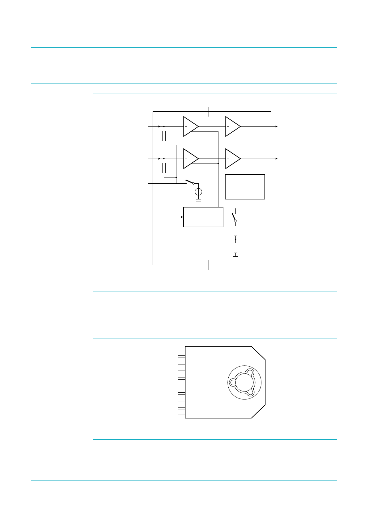
6. Block diagram
IN1
TFA9843AJ
20 W stereo power amplifier with volume control
V
CC
9
4
60
kΩ
8
OUT1
Fig 1. Block diagram
7. Pinning information
7.1 Pinning
IN2
CIV
VC
1
60
kΩ
3
V
REF
7
VOLUME
CONTROL
SHORT-CIRCUIT
AND
TEMPERATURE
PROTECTION
V
CC
0.5V
TFA9843AJ
5
GND
CC
001aae428
2
OUT2
6
SVR
1
IN2
2
OUT2
3
CIV
4
IN1
5
GND
SVR
VC
OUT1
V
CC
TFA9843AJ
6
7
8
9
001aae429
Fig 2. Pin configuration
TFA9843AJ_1 © Koninklijke Philips Electronics N.V. 2006. All rights reserved.
Preliminary data sheet Rev. 01 — 28 April 2006 3 of 19
Page 4

Philips Semiconductors
7.2 Pin description
Table 3. Pin description
Symbol Pin Description
IN2 1 input 2
OUT2 2 loudspeaker terminal 2
CIV 3 common input voltage decoupling
IN1 4 input 1
GND 5 ground
SVR 6 half supply voltage decoupling (ripple rejection)
VC 7 volume control input (standby, mute and volume control)
OUT1 8 loudspeaker terminal 1
V
CC
8. Functional description
TFA9843AJ
20 W stereo power amplifier with volume control
9 supply voltage
8.1 Input configuration
The input cut-off frequency is as follows:
f
i3dB–()
=
---------------------------- -
2π R
1
×()
iCi
Single-ended application: Ri=60kΩ and Ci= 220 nF:
f
i3dB–()
---------------------------------------------------------------- -
2π 60 10
1
3
× 220× 109–×()
12 Hz==
As shown in Equation 2, large capacitor values for the inputs are not necessary; therefore
switch-on delay during charging of the input capacitors can be minimized. This results in a
good low frequency response and good switch-on behavior.
The TFA9843AJ has clamps on the inputs. In Standby mode the voltage on the input pins
is clamped for voltages lower than −0.1 V. When the TFA9843AJ is in Mute, Volume
control or Operating mode (maximum gain) the input clamp voltage is 1 V (RMS).
8.2 Power amplifier
The power amplifier is a single-ended amplifier with an all NPN output stage, capable of
delivering a peak output current of 4 A.
(1)
(2)
8.2.1 Output power measurement
The output power as a function of the supply voltage is measured on the output pins at
THD=10%;seeFigure 7. The maximum output power is limited by the supply voltage of
26 V and the maximum availableoutput current is 4 A repetitive peak current. A minimum
load of 3 Ω is required for supply voltages > 22 V; see Figure 4. The output power is
measured with one channel driven.
TFA9843AJ_1 © Koninklijke Philips Electronics N.V. 2006. All rights reserved.
Preliminary data sheet Rev. 01 — 28 April 2006 4 of 19
Page 5

Philips Semiconductors
8.2.2 Headroom
Typical CD music requires at least 12 dB (factor 15.85) dynamic headroom, compared to
the average power output, for transferring the loudest parts without distortion. At
VCC= 18 V and Po= 6.5 W (SE with RL=4Ω) at THD < 0.5 % (see Figure 5), the
Average Listening Level (ALL) music power without any distortion yields:
TFA9843AJ
20 W stereo power amplifier with volume control
P
oALLSE,()
6.5
-------------
15.85
410 mW==
The power dissipation can be derived from Figure 8 (SE) for 0 dB respectively 12 dB
headroom; see Table 4.
For the average listening level a power dissipation of 4.2 W can be used for a heatsink
calculation.
Table 4. Power rating as function of headroom
Headroom Power output (THD < 0.5 %)
(SE)
0dB P
12 dB P
= 6.5 W 8.2 W
o
= 410 mW 4.2 W
o(ALL)
Power dissipation (P);
both channels driven
8.3 Mode selection
The TFA9843AJ has four functional modes, which can be selected by applying the proper
DC voltage to pin VC; see Table 5.
Table 5. Mode selection
V
I(VC)
0 V to 0.8 V Standby
1.2 V to 1.5 V Mute in this mode the amplifier is DC-biased but not
1.5 V to 5.0 V Volume control in this mode the volume of the amplifier can be
5.0 V to V
CC
Status Definition
in this mode the current consumption is very low
and the outputs are floating; the device is in
Standby mode when V
I(VC)
< 0.8 V
operational (no audio output); this allows the input
coupling capacitors to be charged to avoid plop
noise; the device is in Mute mode when
1.2V<V
I(VC)
< 1.5 V
controlled; the gain can be adjusted between the
range of 1.5V<V
On (maximum gain) in this mode the amplifier has its maximum gain; the
Operating mode is activated at V
I(VC)
< 5.0 V
I(VC)
> 5.0 V
(3)
8.4 Supply voltage ripple rejection
The supply voltage ripple rejection (SVRR) is measured with an electrolytic capacitor of
150 µF connected to pin SVR with a bandwidth of 20 Hz to 22 kHz. The SVRR as a
function of the frequency is illustrated in Figure 10. A larger capacitor value on pin SVR
improves the ripple rejection behavior at the lower frequencies.
TFA9843AJ_1 © Koninklijke Philips Electronics N.V. 2006. All rights reserved.
Preliminary data sheet Rev. 01 — 28 April 2006 5 of 19
Page 6

Philips Semiconductors
8.5 Built-in protection circuits
The TFA9843AJ contains two types of temperature sensors; one measures the local
temperatures of the power stages and one measures the global chip temperature. At a
local temperature of the power stage of approximately 185 °C or a global temperature of
approximately 150 °C this detection circuit switches off the power stages for 2 ms. When
the outputs are switched off the voltage is measured on the outputs. In the event of a
short-circuit to ground or to VCC the device will remain in Protection mode. In all other
cases the power stages switch-on automatically and the detection will take place again;
however a too high temperature will switch-off the power stages immediately. This can
result in repetitive switching during too high junction temperature. This protects the
TFA9843AJ against short-circuits to ground, to the supply voltage, across the load and too
high chip temperatures.
The protection will only be activated when necessary, so even during a short-circuit
condition, a certain amount of (pulsed) current will still flow through the short-circuit (as
much as the power stage can handle without exceeding the critical temperature level).
9. Limiting values
TFA9843AJ
20 W stereo power amplifier with volume control
Table 6. Limiting values
In accordance with the Absolute Maximum Rating System (IEC 60134).
Symbol Parameter Conditions Min Max Unit
V
CC
V
I
I
ORM
T
stg
T
amb
P
tot
V
CC(scp)
supply voltage operating −0.3 +28 V
input voltage −0.3 VCC+ 0.3 V
repetitive peak output current - 4 A
storage temperature non-operating −55 +150 °C
ambient temperature operating −40 +85 °C
total power dissipation - 35 W
short-circuit protection supply
voltage
10. Thermal characteristics
Table 7. Thermal characteristics
Symbol Parameter Conditions Value Unit
R
R
th(j-a)
th(j-c)
thermal resistance from
junction to ambient
thermal resistance from
junction to case
-26 V
in free air 40 K/W
both channels
driven
2.0 K/W
TFA9843AJ_1 © Koninklijke Philips Electronics N.V. 2006. All rights reserved.
Preliminary data sheet Rev. 01 — 28 April 2006 6 of 19
Page 7

Philips Semiconductors
11. Static characteristics
Table 8. Static characteristics
VCC =18V; T
unless otherwise specified.
Symbol Parameter Conditions Min Typ Max Unit
V
CC
I
q
I
CC(stb)
V
O
V
I(VC)
I
I(VC)
[1] A minimum load of 3 Ω is allowed at supply voltages > 22 V.
[2] The DC output voltage with respect to ground is approximately 0.5VCC.
amb
supply voltage operating
quiescent current RL= ∞ - 60 100 mA
standby supply current VCC = 18 V;
output voltage
input voltage on pin VC On mode (maximum
input current on pin VC 0V < V
=25°C; RL=4Ω; V
TFA9843AJ
20 W stereo power amplifier with volume control
I(VC)=VCC
V
I(VC)
gain)
Volume control mode 1.5 - 5.0 V
Mute mode 1.2 - 1.5 V
Standby mode 0 - 0.8 V
; Vi= 0 V; measured in test circuit of Figure 11;
[1]
9 1828V
- - 150 µA
< 0.8 V
[2]
-9-V
5.0 - V
I(VC)<VCC
--20µA
CC
V
12. Dynamic characteristics
Table 9. Dynamic characteristics SE
VCC =18V; T
unless otherwise specified.
Symbol Parameter Conditions Min Typ Max Unit
P
o
THD total harmonic
G
v(max)
∆G
v
V
i
Z
i
V
n(o)
SVRR supply voltage ripple
V
o(mute)
α
cs
|∆G
| maximum voltage gain
v(max)
=25°C; RL=4Ω; f = 1 kHz; V
amb
output power THD = 10 %; RL=4Ω 7 8.5 - W
distortion
maximum voltage gain V
voltage gain range 1.5 V < V
input voltage gain = 0 dB;
input impedance 40 60 - kΩ
noise output voltage
rejection
mute output voltage
channel separation ZS=0Ω 50 60 - dB
difference
I(VC)=VCC
THD = 0.5 %; R
=22V;
V
CC
THD = 10 %; R
= 1 W - 0.1 0.5 %
P
o
> 5.0 V 25 26 27 dB
I(VC)
I(VC)
; measured in test circuit of Figure 11;
=4Ω - 6.5 - W
L
-14-W
=4Ω
L
< 5.0 V - 80 - dB
1.0 - V
THD < 1 %
[1]
- 150 - µV
f
ripple
f
ripple
= 1 kHz
= 100 Hz to
[2]
-60-dB
[2]
-60-dB
20 kHz
[3]
- - 150 µV
--1dB
TFA9843AJ_1 © Koninklijke Philips Electronics N.V. 2006. All rights reserved.
Preliminary data sheet Rev. 01 — 28 April 2006 7 of 19
Page 8

Philips Semiconductors
[1] The noise output voltage is measured at the output in a frequency range from 20 Hz to 22 kHz
(unweighted), with a source impedance ZS=0Ω at the input.
[2] Supply voltage ripple rejection is measured at the output, with a source impedance ZS=0Ω at the input
and with a frequency range from 20 Hz to 22 kHz (unweighted). The ripple voltage is a sine wave with a
frequency f
[3] Output voltage inMutemode(V
to 22 kHz, including noise.
TFA9843AJ
20 W stereo power amplifier with volume control
and an amplitude of 300 mV (RMS), which is applied to the positive supply rail.
ripple
= 1.35 V) and an input voltage of 1 V (RMS) in a bandwidth from 20 Hz
I(VC)
V
I(VC)
001aae340
(V)
50
G
V
(dB)
0
−50
−100
−150
0 6.04.02.0
VCC = 18 V THD = 10 %
Fig 3. Voltage gain as a function of volume control
voltage
10
THD + N
(%)
2
10
mce488
3 Ω2 Ω
4 Ω
8 Ω
24
V
CC
mce485
(V)
P
(W)
60
o
40
20
RL = 1 Ω
0
8
12 28
16 20
Fig 4. Output power (one channel) as a function of
supply voltage for various loads
10
THD+N
(%)
1
001aaa446
1
−1
10
−1
10
−2
10
−1
10
110
(W)
P
o
2
10
−2
10
10
2
10
3
10
4
10
f (Hz)
5
10
VCC = 18 V; f = 1 kHz; RL = 4 Ω VCC = 18 V; Po = 1 W; RL = 4 Ω
Fig 5. Total harmonic distortion-plus-noise as a
function of output power
TFA9843AJ_1 © Koninklijke Philips Electronics N.V. 2006. All rights reserved.
Fig 6. Total harmonic distortion-plus-noise as a
function of frequency
Preliminary data sheet Rev. 01 — 28 April 2006 8 of 19
Page 9

Philips Semiconductors
TFA9843AJ
20 W stereo power amplifier with volume control
V
CC
mce491
(V)
10
P
tot
(W)
8
6
4
2
0
020
4
50
P
o
(W)
40
30
20
10
0
828
12
16 20 24
81216
mce507
(W)
P
o
THD = 10 %; RL = 4 Ω; f = 1 kHz VCC = 18 V; RL = 4 Ω
Fig 7. Output power as a function of supply voltage Fig 8. Total powerdissipationasafunctionofchannel
output power per channel (worst case, both
channels driven)
mce497
α
(dB)
−20
0
cs
mce495
SVRR
(dB)
−20
0
−40
−40
−60
−80
−100
10
2
10
3
10
4
10
f (Hz)
5
10
VCC = 18 V; RL = 4 Ω VCC = 18 V; ZS = 0 Ω; V
−60
−80
10
2
10
3
10
ripple
10
= 300 mV (RMS); a
4
f (Hz)
5
10
bandpass filter of 20 Hz to 22 kHz has been applied;
inputs short-circuited.
Fig 9. Channel separation as a function of frequency
(no bandpass filter applied)
TFA9843AJ_1 © Koninklijke Philips Electronics N.V. 2006. All rights reserved.
Fig 10. Supply voltage ripple rejection as a function of
frequency
Preliminary data sheet Rev. 01 — 28 April 2006 9 of 19
Page 10

Philips Semiconductors
13. Application information
13.1 Application diagrams
13.1.1 Single-ended application
220 nF
V
i
IN1
TFA9843AJ
20 W stereo power amplifier with volume control
V
V
CC
9
4
60 kΩ
8
100 nF
OUT1
1000 µF
+
−
1000 µF
R
L
4 Ω
CC
220 nF
V
i
MICRO-
CONTROLLER
22 µF 10 µF
IN2
CIV
VC
1
60 kΩ
3
V
REF
7
VOLUME
CONTROL
TFA9843AJ
5
GND
SHORT-CIRCUIT
AND
TEMPERATURE
PROTECTION
V
CC
0.5V
CC
OUT2
2
SVR
6
001aae430
1000 µF
150 µF
−
+
R
L
4 Ω
−
Fig 11. SE application diagram
Remark: By switching inductive loads, the output voltage can rise beyond the maximum
supply voltage of 28 V. At high supply voltage it is recommended to use (Schottky) diodes
between the supply voltage and ground.
TFA9843AJ_1 © Koninklijke Philips Electronics N.V. 2006. All rights reserved.
Preliminary data sheet Rev. 01 — 28 April 2006 10 of 19
Page 11

Philips Semiconductors
13.1.2 Volume control drive options
Fig 12. Volume control drive circuit with 3.3 V PWM
GND
PWM
3.3 V
R1
10 kΩ
D1
5.6 V
R5
1 kΩ
TFA9843AJ
20 W stereo power amplifier with volume control
V
CC
T1
5 V
T2
R2
1 kΩ
T3
R3
1 kΩ
R4
1 kΩ
VC
C1
10 µF
001aae337
PWM
5 V
R4
1 kΩ
C1
10 µF
Fig 13. Volume control drive circuit with 5 V PWM
V
CC
R1
10 kΩ
T1
D1
10 V
R5
16 kΩ
R6
16 kΩ
Fig 14. Volume control drive circuit with potentiometer
VC
001aae338
C1
10 µF
VC
001aae339
TFA9843AJ_1 © Koninklijke Philips Electronics N.V. 2006. All rights reserved.
Preliminary data sheet Rev. 01 — 28 April 2006 11 of 19
Page 12

Philips Semiconductors
13.2 Printed-circuit board
13.2.1 Layout and grounding
To obtain a high-level system performance, certain grounding techniques are essential.
The input reference grounds have to be tied with their respective source grounds and
must have separate tracks from the power ground tracks; this will prevent the large output
signal currents from interfering with the small AC input signals. The small-signal ground
tracks should be physically located as far as possible from the power ground tracks.
Supply and output tracks should be as wide as possible for delivering maximum output
power.
TFA9843AJ
20 W stereo power amplifier with volume control
BTL1/2
1000 µF
−SE2+
CIV
22
µF
CIV
Fig 15. Printed-circuit board layout (single-sided); components view
13.2.2 Power supply decoupling
AUDIO POWER CS NIJMEGEN
TVA
TFA9843J
1
100 nF
220
nF
SGND
IN2+ IN1+
220
nF
27 Jan. 2003 / FP
1000 µF
+V
P
SVR
1000 µF
150 µF
10
kΩ
−SE1+
SVR
MODE
10 kΩ
SB ON
MUTE
mce506
Proper supply bypassing is critical for low-noise performance and high supply voltage
ripple rejection. The respective capacitor location should be as close as possible to the
deviceand connected to the power ground. Proper power supply decoupling also prevents
unwanted oscillations.
For suppressing higher frequency transients (spikes) on the supply rail a capacitor with
low ESR (typical 100 nF) has to be placed as close as possible to the device. For
suppressing lower frequency noise and ripple signals, a large electrolytic capacitor (e.g.
1000 µF or greater) must be placed close to the device.
The bypass capacitor connected to pin SVR reduces the noise and ripple on the mid rail
voltage. For good THD and noise performance, a low ESR capacitor is recommended.
TFA9843AJ_1 © Koninklijke Philips Electronics N.V. 2006. All rights reserved.
Preliminary data sheet Rev. 01 — 28 April 2006 12 of 19
Page 13

Philips Semiconductors
13.3 Thermal behavior and heatsink calculation
TFA9843AJ
20 W stereo power amplifier with volume control
The measured maximum thermal resistance of the IC package, R
th(j-mb)
, is 2.0 K/W.
A calculation for the heatsink can be made, with the following parameters:
T
amb(max)
=60°C (example)
VCC= 18 V and RL=4Ω (SE)
T
= 150 °C (specification)
j(max)
R
is the total thermal resistance between the junction and the ambient including the
th(tot)
heatsink. This can be calculated using the maximum temperature increase divided by the
power dissipation:
R
th(tot)
=(T
j(max)
− T
amb(max)
)/P
At VCC= 18 V and RL=4Ω (2 × SE) the measured worst case sine wave dissipation is
8.4 W; see Figure 8. For T
= 150 °C the temperature raise, caused by the power
j(max)
dissipation, is: 150 − 60=90°C:
P × R
R
th(tot)
R
th(h-a)=Rth(tot)
=90°C
th(tot)
= 90/8.4 K/W = 10.7 K/W
− R
= 10.7 K/W − 2.0 K/W = 8.7 K/W
th(j-mb)
This calculation is for an application at worst case (stereo) sine wave output signals. In
practice music signals will be applied, which decreases the maximum power dissipation to
approximately half of the sine wave power dissipation; see Section 8.2.2. This allows the
use of a smaller heatsink:
P × R
R
th(tot)
R
th(h-a)=Rth(tot)
=90°C
th(tot)
= 90/4.2 K/W = 21.4 K/W
− R
= 21.4 K/W − 2.0 K/W = 19.4 K/W
th(j-mb)
TFA9843AJ_1 © Koninklijke Philips Electronics N.V. 2006. All rights reserved.
Preliminary data sheet Rev. 01 — 28 April 2006 13 of 19
Page 14

Philips Semiconductors
TFA9843AJ
20 W stereo power amplifier with volume control
mce504
(5)
V
CC
(1) RL = 2 Ω
(2) RL = 4 Ω
(3) RL = 6 Ω
(4) RL = 8 Ω
(5) RL = 16 Ω
2 × SE loads; T
150
T
j
(˚C)
100
50
0
8
=25°C; external heatsink of 10 K/W; music signals.
amb
(1) (2) (3) (4)
12 28
16 20 24
Fig 16. Junction temperature as a function of supply voltage
(V)
14. Test information
14.1 Quality information
The
General Quality Specification for Integrated Circuits, SNW-FQ-611
is applicable.
TFA9843AJ_1 © Koninklijke Philips Electronics N.V. 2006. All rights reserved.
Preliminary data sheet Rev. 01 — 28 April 2006 14 of 19
Page 15

Philips Semiconductors
15. Package outline
TFA9843AJ
20 W stereo power amplifier with volume control
DBS9P: plastic DIL-bent-SIL power package; 9 leads (lead length 12/11 mm); exposed die pad
q
non-concave
x
D
D
D
1
P
k
q
2
E
view B: mounting base side
A
2
B
E
h
h
1
q
SOT523-1
L
3
L
2
L
2
3.8
3.6
1
v M
v
w
0.8
0.3
ISSUE DATE
00-07-03
03-03-12
x
0.02
Z
1.65
1.10
(1)
19
D
3.5
e
1
E
3.5
b
e
h
2.54
e
(1)
h
14.7
14.3
Z
DIMENSIONS (mm are the original dimensions)
(2)
UNIT b
A
p
2
2.7
mm
Notes
1. Plastic or metal protrusions of 0.25 mm maximum per side are not included.
2. Plastic surface within circle area D1 may protrude 0.04 mm maximum.
0.80
2.3
0.65
OUTLINE
VERSION
SOT523-1
cD
0.58
0.48
(1)
(2)
D
1
13.2
6.2
12.8
5.8
IEC JEDEC JEITA
w M
p
0 10 mm5
scale
e
e
1
2
1.27
5.08 4.85
REFERENCES
Lq
3212.4
11.0
L
11.4
10.0
L
Qc
m
L
L
m
2.8
Pk
3.4
3.1
1
2
3
6.7
4.5
5.5
3.7
e
QE
q
1.15
17.5
0.85
16.3
EUROPEAN
PROJECTION
2
q
1
Fig 17. Package outline SOT523-1 (DBS9P)
TFA9843AJ_1 © Koninklijke Philips Electronics N.V. 2006. All rights reserved.
Preliminary data sheet Rev. 01 — 28 April 2006 15 of 19
Page 16

Philips Semiconductors
16. Soldering
16.1 Introduction to soldering through-hole mount packages
This text gives a brief insight to wave,dip and manual soldering. A more in-depth account
of soldering ICs can be found in our
(document order number 9398 652 90011).
Wave soldering is the preferred method for mounting of through-hole mount IC packages
on a printed-circuit board.
16.2 Soldering by dipping or by solder wave
Driven by legislation and environmental forces the worldwide use of lead-free solder
pastes is increasing. Typical dwell time of the leads in the wave ranges from
3 seconds to 4 seconds at 250 °C or 265 °C, depending on solder material applied, SnPb
or Pb-free respectively.
The total contact time of successive solder waves must not exceed 5 seconds.
TFA9843AJ
20 W stereo power amplifier with volume control
Data Handbook IC26; Integrated Circuit Packages
The device may be mounted up to the seating plane, but the temperature of the plastic
body must not exceed the specified maximum storage temperature (T
printed-circuit board has been pre-heated, forced cooling may be necessary immediately
after soldering to keep the temperature within the permissible limit.
16.3 Manual soldering
Apply the soldering iron (24 V or less) to the lead(s) of the package, either below the
seating plane or not more than 2 mm aboveit. If the temperature of the soldering iron bit is
less than 300 °C it may remain in contact for up to 10 seconds. If the bit temperature is
between 300 °C and 400 °C, contact may be up to 5 seconds.
16.4 Package related soldering information
Table 10. Suitability of through-hole mount IC packages for dipping and wave soldering
methods
Package Soldering method
Dipping Wave
CPGA, HCPGA - suitable
DBS, DIP, HDIP, RDBS, SDIP, SIL suitable suitable
[2]
PMFP
[1] For SDIP packages, the longitudinal axis must be parallel to the transport direction of the printed-circuit
board.
[2] For PMFP packages hot bar soldering or manual soldering is suitable.
- not suitable
stg(max)
[1]
). If the
TFA9843AJ_1 © Koninklijke Philips Electronics N.V. 2006. All rights reserved.
Preliminary data sheet Rev. 01 — 28 April 2006 16 of 19
Page 17

Philips Semiconductors
20 W stereo power amplifier with volume control
TFA9843AJ
17. Revision history
Table 11. Revision history
Document ID Release date Data sheet status Change notice Supersedes
TFA9843AJ_1 20060428 Preliminary data sheet - -
TFA9843AJ_1 © Koninklijke Philips Electronics N.V. 2006. All rights reserved.
Preliminary data sheet Rev. 01 — 28 April 2006 17 of 19
Page 18

Philips Semiconductors
18. Legal information
18.1 Data sheet status
TFA9843AJ
20 W stereo power amplifier with volume control
Document status
Objective [short] data sheet Development This document contains data from the objective specification for product development.
Preliminary [short] data sheet Qualification This document contains data from the preliminary specification.
Product [short] data sheet Production This document contains the product specification.
[1] Please consult the most recently issued document before initiating or completing a design.
[2] The term ‘short data sheet’ is explained in section “Definitions”.
[3] The product status of device(s)described in this document mayhave changedsince this document was publishedand maydiffer incase of multipledevices. Thelatest productstatus
information is available on the Internet at URL
[1][2]
Product status
18.2 Definitions
Draft — The document is a draft version only. The content is still under
internal review and subject to formal approval, which may result in
modifications or additions. Philips Semiconductors does not give any
representations or warranties as to the accuracy or completeness of
information includedherein and shall have noliability for theconsequences of
use of such information.
Short data sheet — A short data sheet is an extract from a full data sheet
with thesame product type number(s)and title. Ashort datasheet is intended
for quickreference only and shouldnot be relied upon to containdetailed and
full information. For detailed and full information see the relevant full data
sheet, which is available on request via the local Philips Semiconductors
sales office.Incase of any inconsistency orconflict with the short data sheet,
the full data sheet shall prevail.
18.3 Disclaimers
General — Information in this document is believed to be accurate and
reliable. However, Philips Semiconductors does not give any representations
or warranties, expressed or implied, as to the accuracy or completeness of
such information and shall have no liability for the consequences of use of
such information.
Right to make changes — Philips Semiconductors reserves the right to
make changes to information published in this document, including without
limitation specifications and product descriptions, at any time and without
notice. Thisdocumentsupersedes and replaces all informationsupplied prior
to the publication hereof.
Suitability for use — Philips Semiconductors products are not designed,
authorized or warranted to be suitable for use in medical, military, aircraft,
space or life support equipment, nor in applications where failure or
[3]
http://www.semiconductors.philips.com.
Definition
malfunction ofaPhilips Semiconductors product canreasonably be expected
to result in personal injury, death or severe property or environmental
damage. Philips Semiconductors accepts no liability for inclusion and/or use
of Philips Semiconductors products in such equipment or applications and
therefore such inclusion and/or use is for the customer’s own risk.
Applications — Applications that are described herein for any of these
products are for illustrative purposes only. Philips Semiconductors makes no
representation or warranty that such applications will be suitable for the
specified use without further testing or modification.
Limiting values — Stress above one or more limiting values (as defined in
the Absolute MaximumRatings System of IEC 60134)may cause permanent
damage tothedevice. Limiting values are stressratings only and operationof
the device at these or any other conditions above those given in the
Characteristics sections of this document is not implied. Exposure to limiting
values for extended periods may affect device reliability.
Terms and conditions of sale — Philips Semiconductors products are sold
subject to the general terms and conditions ofcommercialsale, as published
at
http://www.semiconductors.philips.com/profile/terms, including those
pertaining to warranty, intellectual property rights infringement and limitation
of liability, unless explicitly otherwise agreed to in writing by Philips
Semiconductors. Incaseof any inconsistency orconflictbetween information
in this document and such terms and conditions, the latter will prevail.
No offer to sell or license — Nothing in this document may be interpreted
or construed as an offer to sell products that is open for acceptance or the
grant, conveyance or implicationof any license under any copyrights,patents
or other industrial or intellectual property rights.
18.4 Trademarks
Notice: Allreferenced brands,product names, service namesand trademarks
are the property of their respective owners.
19. Contact information
For additional information, please visit: http://www.semiconductors.philips.com
For sales office addresses, send an email to: sales.addresses@www.semiconductors.philips.com
TFA9843AJ_1 © Koninklijke Philips Electronics N.V. 2006. All rights reserved.
Preliminary data sheet Rev. 01 — 28 April 2006 18 of 19
Page 19

Philips Semiconductors
20. Contents
TFA9843AJ
20 W stereo power amplifier with volume control
1 General description. . . . . . . . . . . . . . . . . . . . . . 1
2 Features . . . . . . . . . . . . . . . . . . . . . . . . . . . . . . . 1
3 Applications . . . . . . . . . . . . . . . . . . . . . . . . . . . . 1
4 Quick reference data . . . . . . . . . . . . . . . . . . . . . 2
5 Ordering information. . . . . . . . . . . . . . . . . . . . . 2
6 Block diagram . . . . . . . . . . . . . . . . . . . . . . . . . . 3
7 Pinning information. . . . . . . . . . . . . . . . . . . . . . 3
7.1 Pinning . . . . . . . . . . . . . . . . . . . . . . . . . . . . . . . 3
7.2 Pin description . . . . . . . . . . . . . . . . . . . . . . . . . 4
8 Functional description . . . . . . . . . . . . . . . . . . . 4
8.1 Input configuration . . . . . . . . . . . . . . . . . . . . . . 4
8.2 Power amplifier. . . . . . . . . . . . . . . . . . . . . . . . . 4
8.2.1 Output power measurement . . . . . . . . . . . . . . . 4
8.2.2 Headroom. . . . . . . . . . . . . . . . . . . . . . . . . . . . . 5
8.3 Mode selection . . . . . . . . . . . . . . . . . . . . . . . . . 5
8.4 Supply voltage ripple rejection . . . . . . . . . . . . . 5
8.5 Built-in protection circuits . . . . . . . . . . . . . . . . . 6
9 Limiting values. . . . . . . . . . . . . . . . . . . . . . . . . . 6
10 Thermal characteristics. . . . . . . . . . . . . . . . . . . 6
11 Static characteristics. . . . . . . . . . . . . . . . . . . . . 7
12 Dynamic characteristics . . . . . . . . . . . . . . . . . . 7
13 Application information. . . . . . . . . . . . . . . . . . 10
13.1 Application diagrams . . . . . . . . . . . . . . . . . . . 10
13.1.1 Single-ended application . . . . . . . . . . . . . . . . 10
13.1.2 Volume control drive options. . . . . . . . . . . . . . 11
13.2 Printed-circuit board . . . . . . . . . . . . . . . . . . . . 12
13.2.1 Layout and grounding. . . . . . . . . . . . . . . . . . . 12
13.2.2 Power supply decoupling . . . . . . . . . . . . . . . . 12
13.3 Thermal behavior and heatsink calculation . . 13
14 Test information. . . . . . . . . . . . . . . . . . . . . . . . 14
14.1 Quality information . . . . . . . . . . . . . . . . . . . . . 14
15 Package outline . . . . . . . . . . . . . . . . . . . . . . . . 15
16 Soldering . . . . . . . . . . . . . . . . . . . . . . . . . . . . . 16
16.1 Introduction to soldering through-hole mount
packages . . . . . . . . . . . . . . . . . . . . . . . . . . . . 16
16.2 Soldering by dipping or by solder wave . . . . . 16
16.3 Manual soldering . . . . . . . . . . . . . . . . . . . . . . 16
16.4 Package related soldering information . . . . . . 16
17 Revision history. . . . . . . . . . . . . . . . . . . . . . . . 17
18 Legal information. . . . . . . . . . . . . . . . . . . . . . . 18
18.1 Data sheet status . . . . . . . . . . . . . . . . . . . . . . 18
18.2 Definitions. . . . . . . . . . . . . . . . . . . . . . . . . . . . 18
18.3 Disclaimers . . . . . . . . . . . . . . . . . . . . . . . . . . . 18
18.4 Trademarks. . . . . . . . . . . . . . . . . . . . . . . . . . . 18
19 Contact information . . . . . . . . . . . . . . . . . . . . 18
20 Contents. . . . . . . . . . . . . . . . . . . . . . . . . . . . . . 19
Please be aware that important notices concerning this document and the product(s)
described herein, have been included in section ‘Legal information’.
© Koninklijke Philips Electronics N.V. 2006. All rights reserved.
For more information, please visit: http://www.semiconductors.philips.com.
For sales office addresses, email to: sales.addresses@www.semiconductors.philips.com.
Date of release: 28 April 2006
Document identifier: TFA9843AJ_1
 Loading...