

Page 1

Colour Television Chassis
TF1.1E
AA
E_15310_000.eps
301104
Contents Page
1. Technical Specifications, Connections, and Chassis
Overview 2
2. Safety Instructions, Warnings, and Notes 4
3. Directions for Use 5
4. Mechanical Instructions 9
5. Service Modes, Error Codes, and Fault Finding 12
6. Block Diagrams, Test Point Overviews, and
Waveforms
Wiring Diagram 15
Block Diagram Video, Audio, and Control 16
I2C Diagram 17
7. Circuit Diagrams and PWB Layouts Diagram PWB
Main Panel: Micro Controller (A1) 18 24
Main Panel: Video Decoder (A2) 19 24
Main Panel: Tuner (A3) 20 24
Main Panel: Video Processor (A4) 21 24
Main Panel: Sound Decoder + Amplifier (A5) 22 24
Main Panel: Power Supply (A6) 23 24
Main Panel: SCART (A7) 23 24
LCD TV AV Front (D) 25 25
Keyboard (E) 26 26
8. Alignments 27
9. Circuit Descriptions, Abbreviation List, and IC Data
Sheets 28
Abbreviation list 29
IC Data Sheets 31
10. Spare Parts List 35
11. Revision List 37
©
Copyright 2005 Philips Consumer Electronics B.V. Eindhoven, The Netherlands.
All rights reserved. No part of this publication may be reproduced, stored in a
retrieval system or transmitted, in any form or by any means, electronic,
mechanical, photocopying, or otherwise without the prior permission of Philips.
Published by JH 05612 Service PaCE Printed in the Netherlands Subject to modification EN 3122 785 15131
Page 2
EN 2 TF1.1E AA1.
Technical Specifications, Connections, and Chassis Overview
1. Technical Specifications, Connections, and Chassis Overview
Index of this chapter:
1.1 Technical Specifications
1.2 Connection Overview
1.3 Chassis Overview
Note: Figures below can deviate slightly from the actual
situation, due to the different set executions.
1.1 Technical Specifications
1.1.1 Vision
Display type : LCD
Screen size : 14” (37 cm), 4:3
Resolution (HxV pixels) : 640x480
Contrast ratio : 450:1
Light output (cd/m
Response time (ms) : 16
Viewing angle (HxV degrees) : 140x120
Tuning system : PLL
TV Colour systems : PAL B/G, D/K, I
Video playback : NTSC M/N 3.58, 4.43
Supported formats : VGA (640x480)
Channel selections : 100 presets
1.1.2 Sound
Sound systems : FM-stereo B/G
Maximum power (W
1.1.3 Miscellaneous
2
) : 450
: SECAM B/G, D/K, L/L’
: PAL B/G
: SECAM L/L’
:VHF
: UHF
: S-band
: Hyper-band
: NICAM B/G, D/K, I, L
):2 x 2
RMS
1.2 Connection Overview
Note: The following connector colour abbreviations are used
(acc. to DIN/IEC 757): Bk= Black, Bu= Blue, Gn= Green, Gy=
Grey, Rd= Red, Wh= White, and Ye= Yellow.
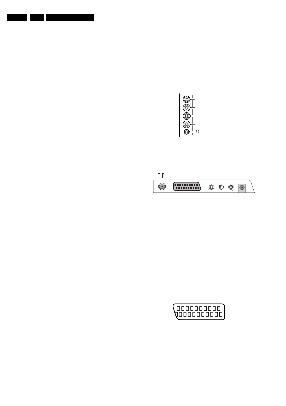
1.2.1 Side Connections
SIDE I/O
S-Video (optional)
Video
L
Audio
R
E_14480_111.eps
060504
Figure 1-1 Side I/O
1.2.2 Rear Connections
EXT1 AV OUT
AUDIOLAUDIO
VIDEO
Figure 1-2 Rear I/O
Aerial - In
- - IEC-type (EU) Coax, 75 ohm D
DC IN
R
E_15310_002.eps
211004
Power supply:
- Mains voltage (V
- Mains frequency (Hz) : 50 / 60
) : 100 - 240
AC
Ambient conditions:
- Temperature range (°C) : +5 to +40
- Maximum humidity : 90% R.H.
Power consumption
- Normal operation (W) : ≈ 40
- Stand-by (W) : < 2
Dimensions (WxHxD in cm) : 34x32x6.3
Weight (kg) : 4.8
Cinch: Video CVBS - Out, Audio - Out
Ye - Video CVBS 1 V
Wh - Audio L 0.5 V
Rd - Audio R 0.5 V
/ 75 ohm kq
PP
/10 kohm kq
RMS
/ 10 kohm kq
RMS
Power: DC - In
1 - 12 V j
External 1: Video RGB/YUV - In, CVBS - In/Out, Audio - In/ Out
21
20
E_06532_001.eps
2
1
050404
Figure 1-3 SCART connector
1 - Audio R 0.5 V
2 - Audio R 0.5 V
3 - Audio L 0.5 V
4 - Ground Audio Gnd H
/ 1 kohm k
RMS
/ 10 kohm j
RMS
/ 1 kohm k
RMS
5 - Ground Blue Gnd H
6 - Audio L 0.5 V
7 - Video Blue/U 0.7 V
/ 10 kohm j
RMS
/ 75 ohm j
PP
Page 3
Technical Specifications, Connections, and Chassis Overview
EN 3TF1.1E AA 1.
8 - Function Select 0 - 2 V: INT
4.5 - 7 V: EXT 16:9
9.5 - 12 V: EXT 4:3 j
9 - Ground Gn Gnd H
10 - n.c.
11 - Video Grn/Y 0.7 or 1 V
12 - n.c.
/ 75 ohm j
PP
13 - Ground Red Gnd H
14 - n.c. H
1.3 Chassis Overview
MAIN PANEL
15 - Video Red/V 0.7 V
16 - RGB Ctrl 0 - 0.4 V: INT
/ 75 ohm j
PP
1 - 3 V: EXT / 75 ohm j
17 - Ground Video Gnd H
18 - Ground RGB Ctrl Gnd H
19 - Video CVBS 1 V
20 - Video CVBS 1 V
21 - Shield Gnd H
/ 75 ohm k
PP
/ 75 ohm j
PP
LCD
REMOTE AND
KEYBOARD PANEL
INVERTER PANEL
SIDE A/V PANEL
E_15310_001.eps
241104
Figure 1-4 Chassis Overview
Page 4

EN 4 TF1.1E AA2.
Safety Instructions, Warnings, and Notes
2. Safety Instructions, Warnings, and Notes
Index of this chapter:
2.1 Safety Instructions
2.2 Warnings
2.3 Notes
2.1 Safety Instructions
Safety regulations require that during a repair:
• Connect the set to the Mains (AC Power) via an isolation
transformer (> 800 VA).
• Replace safety components, indicated by the symbol h,
only by components identical to the original ones. Any
other component substitution (other than original type) may
increase risk of fire or electrical shock hazard.
Safety regulations require that after a repair, the set must be
returned in its original condition. Pay in particular attention to
the following points:
• Route the wire trees correctly and fix them with the
mounted cable clamps.
• Check the insulation of the mains lead for external
damage.
• Check the cabinet for defects, to avoid touching of any
inner parts by the customer.
2.2 Warnings
• All ICs and many other semiconductors are susceptible to
electrostatic discharges (ESD w). Careless handling
during repair can reduce life drastically. Make sure that,
during repair, you are connected with the same potential as
the mass of the set by a wristband with resistance. Keep
components and tools also at this same potential. Available
ESD protection equipment:
– Complete kit ESD3 (small tablemat, wristband,
connection box, extension cable and earth cable) 4822
310 10671.
– Wristband tester 4822 344 13999.
• Be careful during measurements in the high voltage
section.
• Never replace modules or other components while the unit
is switched "on".
• When you align the set, use plastic rather than metal tools.
This will prevent any short circuits and the danger of a
circuit becoming unstable.
2.3.2 Schematic Notes
• All resistor values are in ohms and the value multiplier is
often used to indicate the decimal point location (e.g. 2K2
indicates 2.2 kohm).
• Resistor values with no multiplier may be indicated with
either an "E" or an "R" (e.g. 220E or 220R indicates 220
ohm).
• All capacitor values are given in micro-farads (µ= x10
nano-farads (n= x10
• Capacitor values may also use the value multiplier as the
decimal point indication (e.g. 2p2 indicates 2.2 pF).
• An "asterisk" (*) indicates component usage varies. Refer
to the diversity tables for the correct values.
• The correct component values are listed in the Electrical
Replacement Parts List. Therefore, always check this list
when there is any doubt.
2.3.3 Practical Service Precautions
• It makes sense to avoid exposure to electrical shock.
While some sources are expected to have a possible
dangerous impact, others of quite high potential are of
limited current and are sometimes held in less regard.
• Always respect voltages. While some may not be
dangerous in themselves, they can cause unexpected
reactions that are best avoided. Before reaching into a
powered TV set, it is best to test the high voltage insulation.
It is easy to do, and is a good service precaution.
-9
), or pico-farads (p= x10
-12
-6
),
).
2.3 Notes
2.3.1 General
• Measure the voltages and waveforms with regard to the
chassis (= tuner) ground (H), or hot ground (I), depending
on the tested area of circuitry. The voltages and waveforms
shown in the diagrams are indicative. Measure them in the
Service Default Mode (see chapter 5) with a colour bar
signal and stereo sound (L: 3 kHz, R: 1 kHz unless stated
otherwise) and picture carrier at 475.25 MHz for PAL, or
61.25 MHz for NTSC (channel 3).
• Where necessary, measure the waveforms and voltages
with (D) and without (E) aerial signal. Measure the
voltages in the power supply section both in normal
operation (G) and in stand-by (F). These values are
indicated by means of the appropriate symbols.
• The semiconductors indicated in the circuit diagram and in
the parts lists, are interchangeable per position with the
semiconductors in the unit, irrespective of the type
indication on these semiconductors.
Page 5
3. Directions for Use
l
i
f
C
i
i
n
ff.
#
d
d
l
l.
®
l
.
MENU
l
l
l
he
d
Th
®
b
d
o
l
d
d
h
#
k
h
t
d
.
f
f
:
f
l
.
4
j
.
d
b
d
d
l
d
h
ll
(
)
l
k
s
1
t
f
f
C
t
s
6
h
h
h
d.
b
l
d
h
h
l
d
n
k
l
d
h
d
d
d
d
b
b
h
(
)
f
(
)
d
h
.
i
i
i
i
i
t
i
n
f
C
s
y
f
p
g
h
db
k
h
b
d
d
h
l
ll
d
TV
We
ld
l
d
h
d
h
hl
We
f
i
n
f
C
2
2
2
3
4
4
4
5
6
6
i
n
7
7
i
i
f
i
i
g
l
d
h
bl
b
l
d
l
l
ll
d
l
(
y
)
Directions for Use
EN 5TF1.1E AA 3.
o
s
D Telev
the L
on o
Presentat
eve
ect programmes
just soun
to se
to a
to switch the TV on or o
a
t
e t
y press
e use
taneous
ys to ma
ys can
e
t
e
ose menus, simu
ys.
justment an
an
: to access or c
ect an a
justment
se
t
a
•
rared sensors.
set
On-light and in
Rear o
& é
the
evision
The main connections are made at the bottom o
te
.
a wa
.
wit
ace
rep
an
e remove
can
ustable stand
e stan
For more details on connections see page
Ad
"
!
ier.
ask your dealer
or connecting an ampli
et
soc
socke
supply socke
aeria
mounting kit available as an option
EXT
Audio/Video output
D
EXT1 AV Out DC in
:
ide connection
§ è
'(
ace. To avoid danger
Place your TV on a solid stable sur
on se
s
5 cm
ng the telev
on
t
Pos
e.g.
do not expose the TV to water, or a heat source
5 cm
5 cm
. Do not obstruct the ventilation
e rear
at t
lamp, candle, radiator
gri
e
.
e environment.
o not contai
ut use t
iance
atteries,
e app
consult your distributor
t
wit
mium so as to protect t
t way roun
e rig
ey are t
t
ie
ca
e
atteries supp
e
mercury or nic
your use
iscar
o not
ease
recycling methods available
-type batteries supplied, making sure
Insert the two R
emote contro
this television set.
o
urchasin
or
ou
Thank
Introduct
set.
y.
operate your
an
oroug
it t
p you insta
e
at you rea
to
t
esigne
een
y recommen
as
oo
strong
an
wou
is
action.
hope our technology meets entirely with your satis
D Television . . . . . . . . . . . . . . . . . . . . . . . . . . . . . . . . . . . . .
ontent
the L
o
le o
uick installation . . . . . . . . . . . . . . . . . . . . . . . . . . . . . . . . . . . . . . . . . . . . . . . . . .5
onnecting . . . . . . . . . . . . . . . . . . . . . . . . . . . . . . . . . . . . . . . . . . . . . . . . . . . . . . . .
ositioning the television set . . . . . . . . . . . . . . . . . . . . . . . . . . . . . . . . . . . . . . . . .
Installat
Presentation o
onnecting peripheral equipment . . . . . . . . . . . . . . . . . . . . . . . . . . . . . . . . . . . . . .
Remote control . . . . . . . . . . . . . . . . . . . . . . . . . . . . . . . . . . . . . . . . . . . . . . . . . . . .
witching on . . . . . . . . . . . . . . . . . . . . . . . . . . . . . . . . . . . . . . . . . . . . . . . . . . . . . .
Remote control keys . . . . . . . . . . . . . . . . . . . . . . . . . . . . . . . . . . . . . . . . . . . . . . .
English
on
ormat
o
perat
ther settings in the Install menu . . . . . . . . . . . . . . . . . . . . . . . . . . . . . . . . . . . . .
rogram sort . . . . . . . . . . . . . . . . . . . . . . . . . . . . . . . . . . . . . . . . . . . . . . . . . . . . . .
icture settings . . . . . . . . . . . . . . . . . . . . . . . . . . . . . . . . . . . . . . . . . . . . . . . . . . . .
Manual store . . . . . . . . . . . . . . . . . . . . . . . . . . . . . . . . . . . . . . . . . . . . . . . . . . . . . .
n
cal
ound adjustments . . . . . . . . . . . . . . . . . . . . . . . . . . . . . . . . . . . . . . . . . . . . . . . . .7
ips . . . . . . . . . . . . . . . . . . . . . . . . . . . . . . . . . . . . . . . . . . . . . . . . . . . . . . . . . . . . .
eature settings . . . . . . . . . . . . . . . . . . . . . . . . . . . . . . . . . . . . . . . . . . . . . . . . . . . .
Pract
n
Recycl
ask
iances
.
app
e
e recyc
ect use
e or can
ist companies co
er reusa
.
waste, specia
in your set are eit
s use
e materia
minimise environmenta
our dealer for further details
and dismantle them after retrieving any materials that can be used again
Page 6
EN 6 TF1.1E AA3.
(
n
)
.
C
C
f
C
f
I
h
d
l
d
d
h
l
h
ll
k
.
U
h
l
l
d
l
d
d
h
f
r
l
k
.
A
d.
i
g
k
h
h
W
h
h
l
t
V
d
h
s
Wh
h
d
h
d
h
d
h
TV
t
ll
b
Th
d
d
h
l
e
l.
32
00
O
.
f
/
d
:
”
”
”
”
f
”
O
”
f
f
f
f
f
i
s
ifi
r
i
i
i
t
i
(
)
l
bl
.
i
i
r
f
o
d
bl
d
.
i
r
i
i
k
h
h
i
t
2
6
9
-
+
T
T
O
l
k
s
e
f
n
o
d
S
o
o
o
f
o
h
b
l
I
l
II
9
t
ff
f
.
i
i
y
d
l
h
e
f
°
.
i
d
f
f
d
d
d
.
l
l
o
f
.
)
u
ll
h
.
i
(
4)
ess
seve
al
t
es
to
select
the
q
d
EXT
.
(
o
)
g
f
/
16
9
4
e
h
h
h
Th
d
l
r
h
ll
.
V
d
h
d
l
l
e
h
d.
i
f
i
n
d
l
h
b
r
d
h
h
.
y
h
TV
db
d
To
h
h
TV
s
P
i
g
p
g
s
d
.
b
d
h
d
d
e
f
f
.
f
h
he
f
.
i
e
h
l
d
ro
ramme.
i
s
d
.
,
2
d
b
d
f
.
Directions for Use
the voltage is indicated o
. Only use the AC-DC adaptor supplied with the TV
The TV works with a DC supply
the label
n
onnect
ug
e mains p
or ventilation.
insert t
an
ea
the adaptor to the TV D
et
plug o
aptor power
soc
e a
e wa
onnect the D
nsert t
socket. Leave a space round the adaptor
into t
•
•
e
connect t
an
the TV to you
ie
supp
ea
connection
et
e aeria
socket situated at the bottom o
soc
se t
rrange the leads by passing them through the television
aeria
•
stan
•
e
th decode
or DVD recorder
pmen
ity euroconnector ca
deo recorder
deo recorder w
arry out the connections shown opposite, using a good
V
V
qua
pheral equ
ng per
EXT1 AV Out DC in
onnect
:
deo recorde
V
transmissions
e
the video recorder.You will then be able t
scram
onnect the decoder to the second euroconnector
ecor
socket o
own opposite.
ver, decoder, DVD, games, etc.
e connections as s
te rece
e t
a
atell
pmen
EXT1 AV Out DC in
:
ther equ
ey,
um
se
e
e
S A
ec
se
on t
e soun
,t
ones are connecte
p
one
ea
p
en
ea
S-Video
Video in
L
e vo
just t
to a
ys are use
e
e cut.
wi
Audio in
t
it
own opposite.
e connections as s
e t
a
on
de connect
hms
and 6
IN
AUDI
video connecting cable
the TV set to an
the TV set to a ”VIDEO IN”
i unit.
i unit, use an audio
connect
connect a Hi-
eve
The headphone impedance must be between
an
R
*
EXT1 AV Out DC in
e
:
ier.
outputs o
the Hi-
R
the ampli
and
L
”L” and ”R” o
input o
- The
- The ”VIDEO” output o
Ampl
e.
y mo
to stan
e
set t
tandb
set on again, pres
e
t
witc
,
on
t
tere
Nicam
orce programmes i
an
ound mod
tere
Used to
RADI
ua
ua
etween
or bilingual programmes, t
oose
or,
c
ine
ormats
prede
erent screen
cture and soun
Forma
:
select di
mart p
Used to access a series o
MAR
MAR
ates t
settings
rom the menus
position re
soun
persona
picture an
settings selected
ramme
ro
own a programme
TV
n
move up or
elect
[
e ar
mo
e soun
t
ew seconds
or a
er an
e num
For some TV programmes the title o
displayed
the screen
e programme appears at t
t
bottom o
3
cal key
irect access to programmes
or
Numer
4
e entere
igit must
n
or a 2 digit programme number
the
8
ore the dash disappears
be
0
y viewe
e previous
ous programm
access t
Prev
g
p
ey
p.
p. 8
pherals
elect per
emote contro
connector
decoder, vide
im
uire
r
e
Most equipment
r
.
itsel
spla
e tim
me d
T
ay or remove t
carries out the switchin
isp
recorder
1
en
programme n
transmitted by the teletext o
:
e menus
Format
up or exit t
ursor
keys are used to navigat
ca
These
e
e menus.
t
roug
t
arge o
to en
ys are use
y
e picture vertica
compress t
eve
e soun
just t
a
e
ut
e soun
mute or restore t
o
ormat
n
creen
e programme num
ay t
isp
e timer
e time remaining on t
t
an
Page 7
l
e
i
i
i
u
d
h
dd
h
l
.
h
d
l
h
MENU
t
S
ON
h
h
h
he
l
h
m
l
e
*)
d
h
),
E
e
),
i
d
Ki
d
m
)
e
).
f
(
)
t
h
h
e
O
nce
a
f
.
f
f
y
f
r
l
h
h
to
s.
f
f
8).
f
f
,
d
h
s.
:
h
d
d
b
h
he
s
to
:
h
¬
d
(
)
l
h
h
Wh
h
h
b
d
h
i
.
d
to
d.
h
l
.
h
d
l
he
S
ON
:
:
f
r
h
.
:
(
r
f
f
d
h
l
l
“
”
S
f
l
bl
ll
h
S
ON
a
ears
f
f
b
l
b
d
h
t
b
h
.
f
f
(
8)
f
l
.
U
C
E
D
S
ON
S
e
01
O
E
z
T
e
e
t
ll
h
h
b
f
.
h
y.
MENU
l
d
h
.
S
ON
h
he
h
h
t
.
h
he
d
h
e
f
d
i
s
d
h
.
h
l
i
i
i
n
f
f
,
d
l
d
Th
u
l
h
d
l
e
he
d
f
l
h
h
h
l
o
l
d
l
d
h
f
t
h
“
”
l
l
h
d
l
d
h
h
ll
S
ON
a
ears
ll
.
f
f
l
b
d
h
t
to
b
h
.
f
f
(
8)
f
l
i
.
h
h
h
.
Q
(
d
)
h
l.
i
i
n
CO
E
y
e
G
SH
MENU
C
E
D
S
ON
S
ON
G
SH
GB
S
e
S
e
t
t
requenc
y
you know the
The search starts.
e
ound, the scanning stops
t
y wit
the required programme, enter its numbe
earch
programme is
Go to the next step. I
o
irect
actory
y
e
ound, consult the possible solutions
the reception is not satis
i
just using t
ne tune
no picture is
p.
a
I
t
er wit
num
esire
e
enter t
y
rogram
and the
aracters.
ys to move aroun
e c
5 characters
ect t
e È
ys to se
use t
ame
the name display area
e
press t
een entere
as
t
e name
y to ex
en t
.
e programme is store
epeat steps
tore
times
severa
Directions for Use
or all
or
e
pp
ound have
u
, use t
.
p.
EN 7TF1.1E AA 3.
ere
the programmes
TALLATI
IN
e
y t
ina
automatically.I
y num
een correct
not
em
er t
menu to renum
ound see Tips
times
you want to exit the menus, press
no picture is
I
I
severa
e in your region.
a
e menus press
exit t
e store
to start automatic search
tore
on men
Auto
programmes avai
e
e programmes
a programme to t
to store t
stor
is menu is use
anua
one at a time or to a
ey
e
e set, press t
on t
switc
en t
e
e cursor t
t
ay t
wit
isp
en press
t
y to
TALLATI
ist
e
store
IN
ress t
elec
manua
existing
re
e remote
ey on t
uick Installation chapter.
, press the P
o straight to the
contro
If the TV remains in standby mode
indicator
tor
Manual
rogram
MAIN MEN
TUR
PI
o
...
your
ect
ist, se
e
or the search, automatic
oes not appear in t
Great Britain).This setting is used
programme sort and teletext display. I
country
u
to change the display language
TALLATI
anguage
IN
e menus
t
o
to select your country
ountry
P
un
ne
ame -----
ystem EUR
earch 671 MH
tor
TALLATI
UN
FEATURESIN
I standard
, you must selec
o
urop
ng
(automatic detection
LL’ standard
te
e versions
urop
n
astern
ect
se
yste
ing to t
BG standard
or accor
LL’ standard
or France
ranc
Except
DK standard
ranc
oice
e c
t
n the Installat
ect t
se
ngs
y an
e
ther sett
ress t
t
ate wit
i
e remote contro
va
ys on t
e
ect your country an
se t
se
e
anguage using t
ect your
...
oice
ext se
your country does not appear in the list, selec
I
c
pp
u
y.
TALLATI
ate wit
i
starts automatica
IN
va
e searc
ys an
Finally the
menu
or
e
, use t
ound have not been
ere
y
y num
the programmes
automatica
I
correct
severa
.
p.
ound see Tips
em
er t
um
you want to exit the menus, press
no picture is
I
I
mes
t
e
ress t
e screen
on t
aye
isp
t
menu wit
u
or
e
TALLATI
IN
en t
elect the
cursor t
elect the programme you want to move wit
press
ys an
t
ys to choose the new
k
e
en use t
times.
mes a
severa
as many t
e programmes
irm with
an
e menus, press
to move t
exit t
epeat steps
umber and con
equire
ng o
tch
w
irst time
is men
or the
o
on screen.
aye
nstallat
isp
ck
u
When you turn on the TV set
a menu is
anguag
e country an
ect t
prompts you to se
M
WEL
anguag
ountr
ering
programmes
o
LI
TALLATI
tor
IN
tor
r
ountry
or
Language EN
Auto
Manual
TUR
TALLATI
UN
PI
FEATURESIN
LI
EN
or 5 seconds to
eys on the TV set
e menu.
an
ay t
isp
t
e num
ange t
ow you to c
is menu a
rogramme sor
Page 8
EN 8 TF1.1E AA3.
i
s
i
n
f
e
f
n
h
ll
d
i
e
)
e
l
D
bl
e
(
)
i
e
y
p
p
y?
y
u
(
)
d
f
e
f
.
d
f
o
d
h
h
d
h
h
TV
f
m
(
).
f
y
?
C
f
o
h
h
d
.
f
f
1
y
g
db
d
.
f
t
l
h
dby
(
).
i
g
t
f
f
e
f
-
.
i
?
f
f
s
h
.
f
t
y
'
.
:
Y
ff
f
f
(
)
/
ff
i
g
pa
e
d
ll
l
h
d
d
f
e
3
.
f
e
100
k
).
f
120
r
f
e
d
l
d
R
h
h
.
f
s
S
.
s
i
t
to
i
s
(
).
f
.
4
r
d
.
f
.
l
e
page
f
e
d
h
l
.
e
i
i
i
n
i
n
f
i
n
i
i
n
f
e
t
p
y
l
d
l
Th
k
d
e
b
Th
d
f
.
(
).
ll
l
l
b
.
d
l
d
bl
he
l
d
l
.
3
56 1547.1
i
i
s
j
s
l
t
C
E
d
C
E
a
ears
:
h
l
d
d
.
e
p
to
sto
e
t
e
.
l
h
.
i
i
f
j
i
h
h
h
h
b
ll
.
t
ff
e
h
l
h
d
d
k
.
r
f
l
.
s
e
f
n
h
d
.
l
t
D
D
d
d
l
d
h
l
d
he
d
.
t
e
d
h
h
l
.
i
i
f
i
l
e
f
d
h
k
.
ble
f
.
s
f
.
h
d
d
i
s
l
t
S
s
Y
i
r
l
db
.
k
f
h
TV
.
Y
f
0
11.
d
l
d.
h
k
to
TV
d
l
h
d
d.
l
h
k
to
F
h
h
d
l
P
d
d
f
f
y
d
.
f
f
0
11.
l
h
MENU
C
E
D
S
ON
C
E
g
-
r
e
MENU
C
E
S
ON
D
l
I
-
bl
I
I
-
e
U
C
E
D
S
ON
S
O
F
O
F
P
d
Directions for Use
e an
items that can b
digit page number
amiliar with the
ange to transparent mo
etext, c
te
to ca
.
is is use
then exit.The summary appears with a list o
accessed. Each item has a corresponding
o
on
or viewers with hearing problems or who are not
ress
¤
cable networks, satellite channels, etc.
.
ers access to subtitles
It also o
transmission language
, ente
t, the counter turns and then th
the page required using the
ys. Example:page
will be displayed and the screen will remain blan
the channel selected does not broadcast teletext, th
I
indication
umber is displayed top le
in this case, exit teletext and select another channel
Enter the number o
g
n
elect
9
P
0
ù
¤
ª
SMART
ı
`
-
SMART
Y
MENU
er page
the screen
is operation to view anot
epeat t
elect another number
.
aye
isp
the counter continues to search, this means that the page i
page is
I
ing pages
coloured keys are used to access the items o
Coloured areas are displayed at the bottom o
The
correspon
not transmitted.
rec
tem
D
access
the
P
3
[
- -
12
+ +
”
th
usually page 100
size
lash when the item or the page is not yet available
en return to norma
t
This returns you to the contents page
The coloured areas
This allows you to display the top or bottom part o
page an
arg
n
ontent
Ë
Á
564
879
0
Ë
t
ppears top le
to stop or resum
ication
ey is use
is
e in
y.
successive
aye
-page acquisition.
ertain pages contain sub-pages which are automaticall
isp
su
o
t
s
acqu
top sub-pag
English
games solutions
-page
etext su
ect te
ows you to se
is a
display or hide the concealed information
o
o
dde
H
ormat
a sub-pag
n
o
rect select
D
e or activate t
isa
y
ay
to temporari
isp
is is use
etext
te
o
s
used the audi
heck that you have not con
sound
o
p
T
oor recept
en in stan
5 mins, it automaticall
or
e
io input
y mo
e au
t
the set receives no signal
oes into stan
output wit
StandbyI
n
justing your picture: see F
y a
mountains or high buildings may b
or ghost pictures, echoing or shadows. I
or modify the orientation of the outsid
p.6
is case, try manua
esponsible
The proximity o
t
ree cloth to clean th
itted with components tha
save power,your set is
e you to receiv
oes your antenna ena
.
aeria
your set. Do not use alcohol
t and lint-
ow power consumption w
the se
n
less than 2 W
nly use a clean, so
lean
give it a very
mode
screen and the casing o
?
o
Have
ten the caus
erl
ro
UHF or VHF band
. Poorly connecte
p. 6
ou connected the aerial socket
ctur
broadcasts in this frequency range
No p
Have
chosen the right system?
euroconnector cables or aerial sockets are o
or 30 second
the TV
s after-sales service
ll no results
en reconnect it
t
your TV set breaks down, never attempt to repair i
based or solvent-based products
picture or sound problems.Check all connections
o
ourself: contact your dealer
Disconnect the mains plug o
t
I
e correct
p. 6
ave t
setting
o not
yste
at you
y the
ier connected to the TV does not deliver an
is means t
,t
o soun
on certain channels you receive a picture but n
I
soun
system. Modi
The ampli
111 2
iance
ri
the
e menus
times to exit t
severa
ress
erenc
e picture
ustments:
anges t
is c
t
the ad
this changes the di
tness :
on o
g
pt
ontras
r
tones
ar
t an
ig
e
this changes the intensity o
olou
etween t
justments
e picture a
this changes the pictur
to store t
initio
our
harpnes
tore
co
de
em.
to store t
press
an
nce the adjustments have been made selec
tor
Descr
:
press
TUR
an
PI
pp
ng
TUR
u
htness ---I------
ontrastolou
PI
ec
se
TUR
PI
cture sett
ress
P
harpnesstor
Bri
TUR
TALLATI
UN
PI
FEATURESIN
m
h
ect a setting an
r
ys to se
just
ress
ys to a
e
and
nce the adjustments have been made select
se t
tor
aye
and press
isp
UN
menu is
ustment
soun
ec
se
UN
ress
ound ad
t
times
severa
requency sounds
ngs :
ers
the sett
to balance the sound on the le
e menus press
quit t
on o
pt
anc
a
t spea
this alters the high
rig
e
an
Descr
---
----
------
UN
e ---
ance -----
e
a
ass ------
tor
TUR
TALLATI
PI
SOUNDFEATURESIN
settings.
requency sounds
to store soun
is is use
t
this alters the low
as
tore
ect a setting an
just
ys to se
ys to a
e
se t
t
and pres
ng
FEATURE
ec
se
ress
Feature sett
7
aye
isp
irst time, key the code
e menu is
The
.
is entere
F
set cannot
e
hild Loc
e correct passwor
t
switc
unti
Child Loc
cance
e use
witc
F
F
FEATURE
asswor
hildlock
ew
Timer
MAIN MEN
TUR
TALLATI
UN
FEATURESIN
PI
an
asswor
irm b
ew
ect
e se
time
igure code. Con
e co
ange t
c
enter a new 4
entering a secon
e menus.
times to exit t
7
orgotten your secret code, enter the
severa
ress
you have
I
universal code
y
ect an automatic stan
This menu lets you block use o
to se
set
me
e
hildloc
period
t
T
Page 9
4. Mechanical Instructions
Mechanical Instructions
EN 9TF1.1E AA 4.
Index of this chapter:
4.1 Service Positions
4.2 Assy/Panel Removal
4.3 Set Re-assembly
Notes:
• Figures below can deviate slightly from the actual situation,
due to the different set executions.
• Follow the disassemble instructions in described order.
4.1 Service Positions
For easy servicing of this set, there are a few possibilities
created:
• The buffers from the packaging.
• Foam bars (created for service).
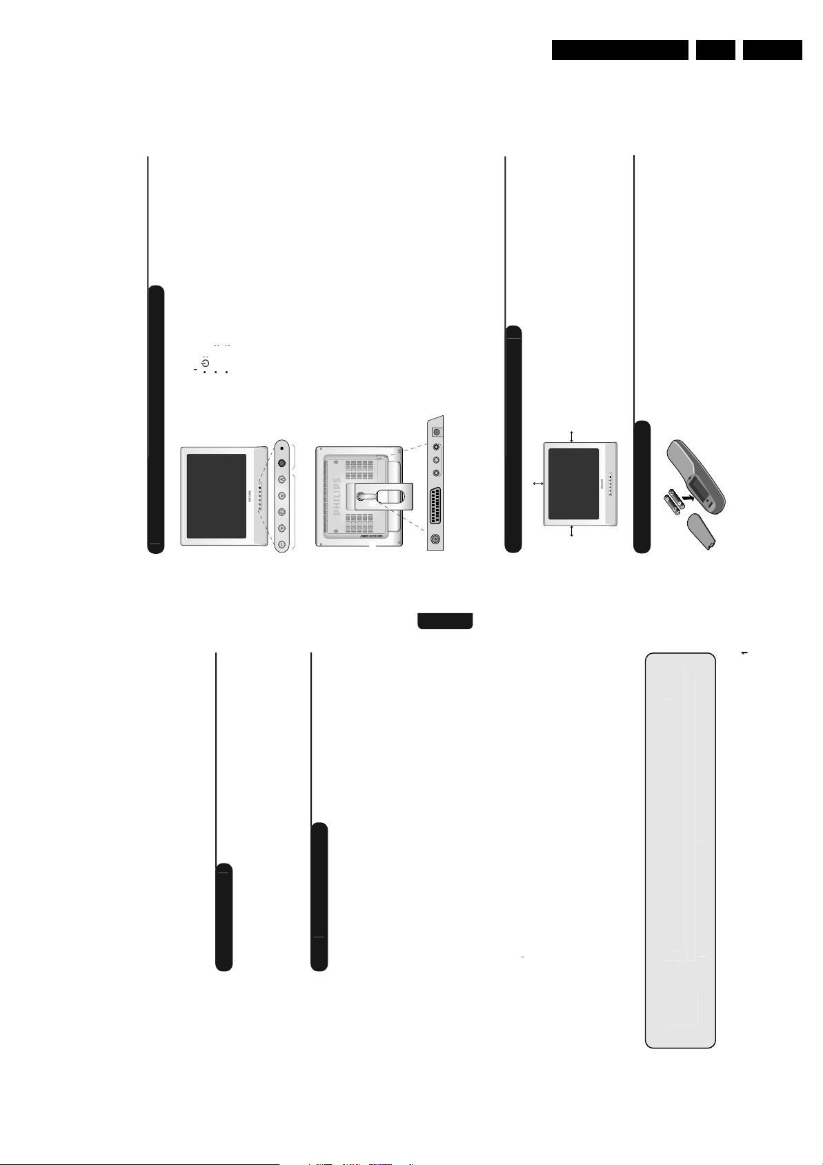
4.1.1 Foam Bars
E_06532_018.eps
Figure 4-1 Foam bars
The foam bars (order code 3122 785 90580 for two pieces) can
be used for all types and sizes of Flat TVs. By laying the TV
face down on the (ESD protective) foam bars, a stable situation
is created to perform measurements and alignments.
By placing a mirror under the TV, you can monitor the screen.
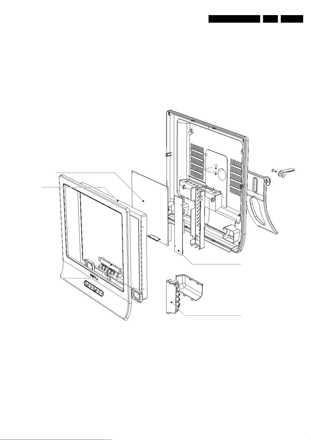
4.2 Assy/Panel Removal
Before removing the cover, turn off LCD TV and plug off the
adapter socket.
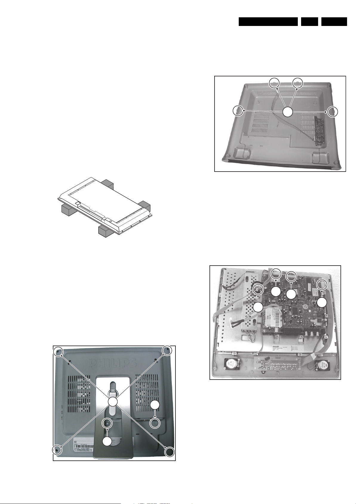
170504
1. Remove the connector cover.
2. Remove the 4 screws at the corner (A) and the two in the
middle (B) that secure the rear cover.
3
Figure 4-3 inside Rear cover
3. Lift the rear cover at the bottom. Be aware of the clamps at
the left and right side and at the top (2x)of the cover.
Make sure that wires are not damaged during cover
removal.
4. Remove the two side AV connectors from the side
connector panel and the headphone connector from the
main panel.
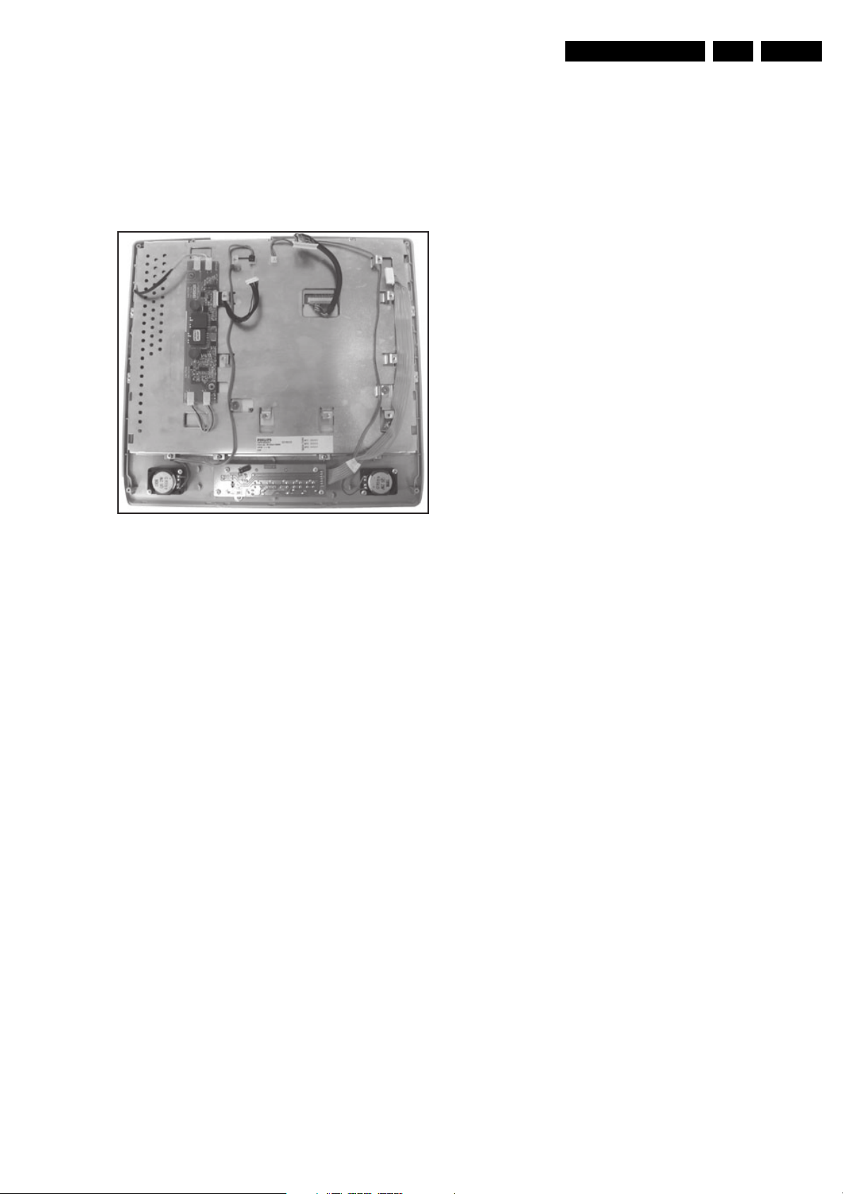
4.2.2 Main Panel
C
D
B
E_15130_004.eps
211004
A
4.2.1 Rear Cover
A
B
Figure 4-2 Rear cover
B
E_15130_003.eps
211004
E_15130_015.eps
051104
Figure 4-4 Main panel
1. Remove connector (A) to remote and keyboard panel.
2. Remove connector (B) to invertor panel.
3. Remove both the speaker connectors (C).
4. Remove connector to LCD panel (D).
Caution: Be careful, because this connection is very
fragile!
5. Remove the 4 screws from the main panel.
6. Take out the panel.
Page 10
EN 10 TF1.1E AA4.
Mechanical Instructions
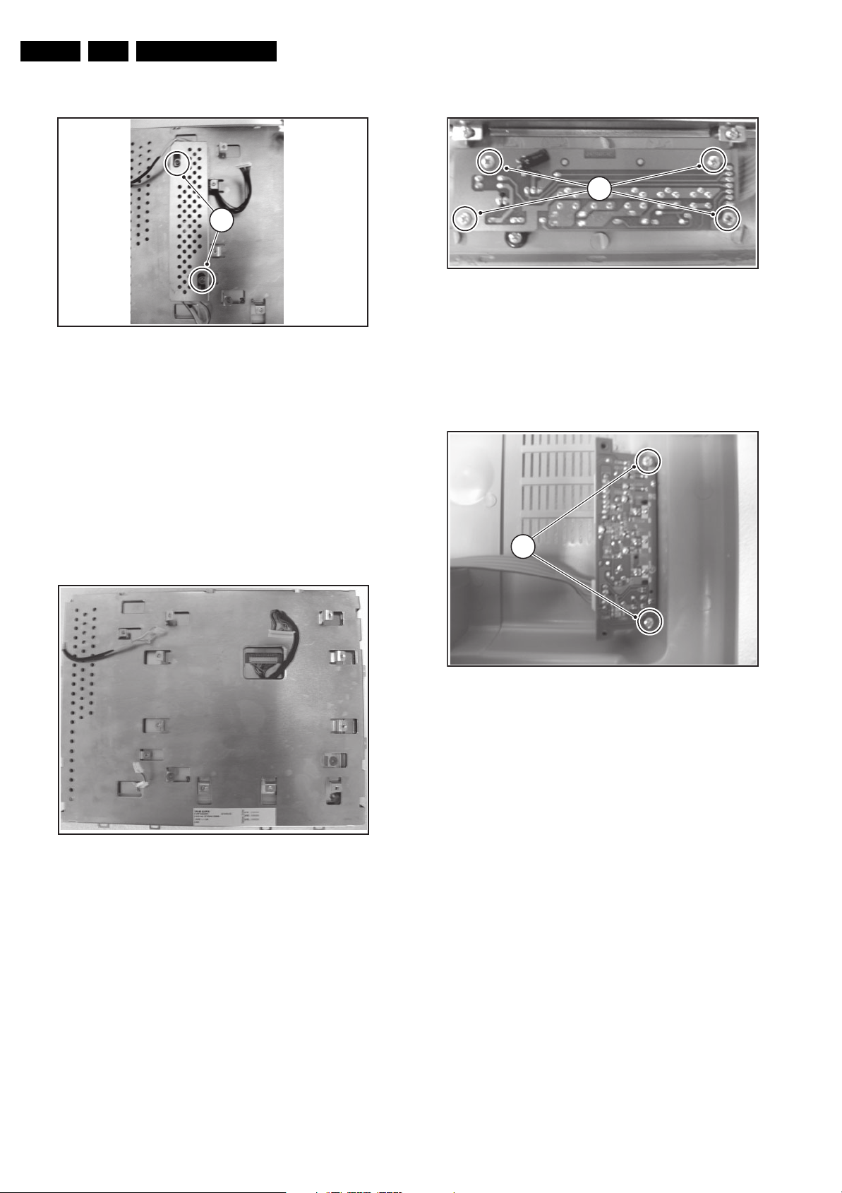
4.2.3 Invertor Panel
2
Figure 4-5 Invertor panel
1. Remove the 4 conncectors to LCD panel.
2. Remove the 2 fixation screws that hold the shield and
Invertor panel.
3. Take out the shield.
4. Take out the panel.
4.2.4 LCD Panel
E_15130_006.eps
221004
4.2.5 Remote and Keyboard Panel
1
Figure 4-7 Remote and Keyboard panel
1. Remove the fixation screws.
2. Take out the panel.
3. Be aware of the buttons, they are not fixed in the frame.
4.2.6 Side Connector Panel
E_15130_008.eps
221004
Important: Be sure to work in a dust free environment during
the following activities. In addition, the use of (fabric) hand
gloves is advised.
E_15130_007.eps
211004
Figure 4-6 LCD panel disassembly
1. Place the TV set face down on the foam bars. Place the
bars at the edges of the set, so they will support the front
frame and not only the glass plate!
2. Remove all the parker screws around the frame.
3. Lift the LCD panel including the metal cover from the
plastic frame.
4. Remove the screws (4) that hold the LCD panel.
5. Remove the LCD panel from the metal cover. Be careful,
don’t damage the cables and be aware of the cable
positions.
2
E_15130_009.eps
Figure 4-8 Side connector panel
1. Disconnect all cables from the panel.
2. Remove the fixation screws and take out the panel.
221004
Page 11
4.3 Set Re-assembly
To re-assemble the whole set, execute all processes in reverse
order.
Notes:
• While re-assembling, make sure that all cables are placed
and connected in their original position. See figure "Cable
dressing".
Mechanical Instructions
EN 11TF1.1E AA 4.
Figure 4-9 Cable dressing
E_15130_010.eps
221004
Page 12

EN 12 TF1.1E AA5.
Service Modes, Error Codes, and Fault Finding
5. Service Modes, Error Codes, and Fault Finding
Index of this chapter:
5.1 Test Points
5.2 Service Mode
5.3 Problems and Solving Tips
5.4 Fault Finding and Repair Tips
5.1 Test Points
This chassis is equipped with test points in the service printing.
In the schematics test points are identified with TPxx. These
test points are specifically mentioned in the service manual as
“half moons” with a dot in the centre.
Perform measurements under the following conditions:
• Television set in Service Mode.
• Video input: Colour bar signal.
• Audio input: 3 kHz left channel, 1 kHz right channel.
5.2 Service Mode
Service mode offers several features for the service technician.
5.2.1 Service Menu
Purpose
• To change option settings.
• To enable / disable hotel mode.
• To perform alignments.
Specifications
• Software version and Option settings display.
• Option settings.
• Software alignments (Geometry and Audio).
• Hotel mode.
• Automatic Gain Control.
How to enter
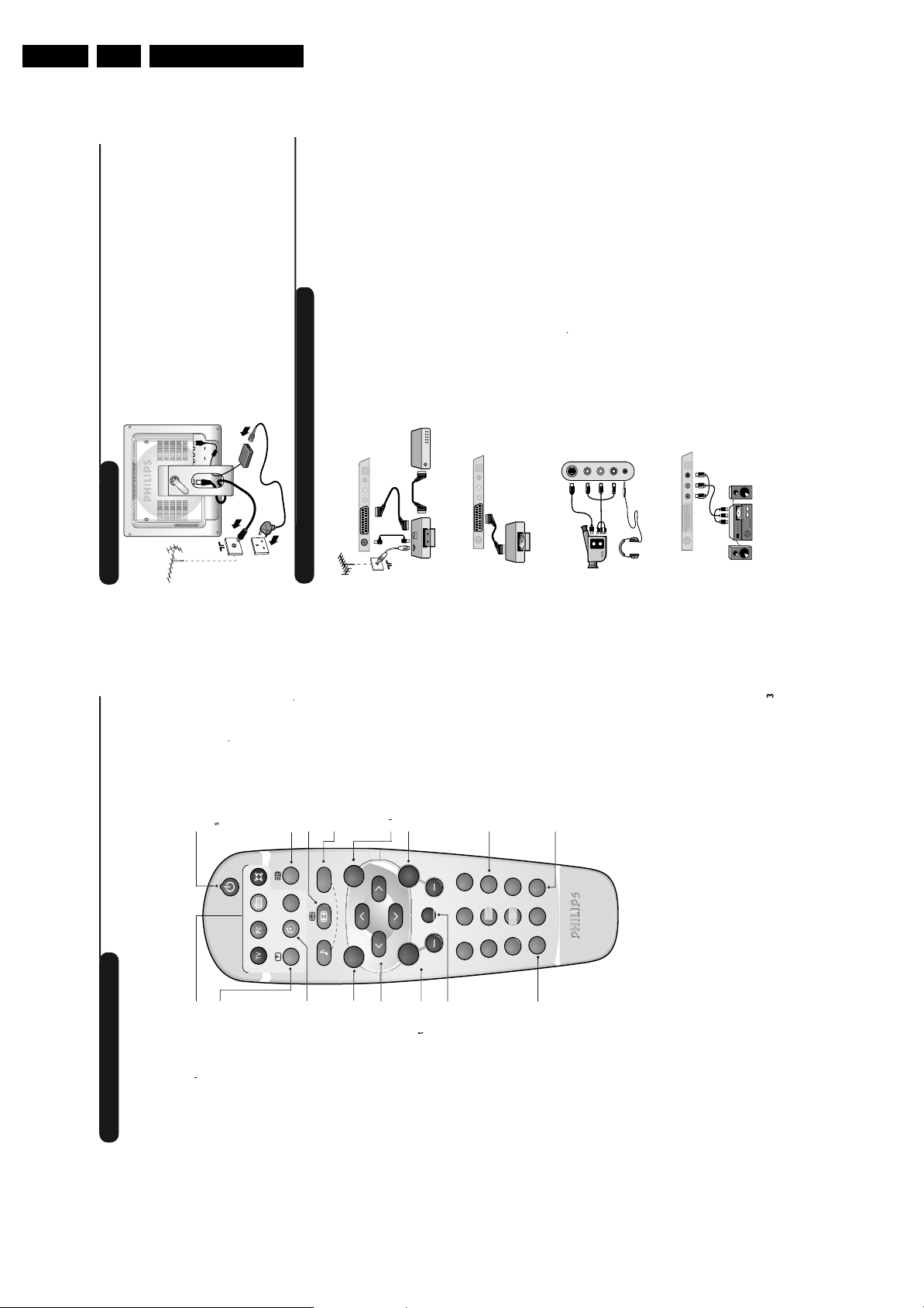
Press the following key sequence on the remote control
transmitter: “062596" directly followed by the OSD/STATUS/
INFO button (do not allow the OSD display to time out between
entries while keying the sequence).
After entering Service Menu, the following screen is visible.
LCD14 pv1.4
Program P01
OPT.
GEO.
Hotel Mode OFF
Volume
AGC 0031
E_15130_011.eps
221004
Menu explanation
1. AAAAA BB X.XX. This is the software identification of the
Main microprocessor:
– A= the chassis name (LCD14).
– B= software identification: pv= Philips Version
– X= the Main software version number (updated with a
major change that is incompatible with previous
versions).
2. Program. Indication of the current program (00..99).
3. Option Bytes (OPT). Shows all option settings. See
“Options” in the Alignments section for a detailed
description. Three codes are available.
4. Geometry (GEO). See Alignments section for a detailed
description.
5. Hotel mode. Used to set the TV in hotel mode.
6. Automatic Gain Control (AGC). Used to adjust the AGC
(00..31). Fixed value =16.
How to navigate
• In the Service Menu, select menu items with the CURSOR
UP/DOWN keys on the remote control transmitter. The
selected item will be highlighted.
• With the CURSOR LEFT/RIGHT keys, it is possible to:
– Activate the selected menu item.
– Change the value of the selected menu item.
– Activate the selected submenu.
• When you press the MENU key in while in a submenu, you
will return to the previous menu.
How to exit
When you press the MENU key in while in a the main service
menu, you will return to the normal user mode.
5.2.2 Hotel Mode
Purpose
Installation is omitted in Hotel Mode. You cannot search any
channel when the Hotel Mode is activated. Volume level cannot
be increased higher then a previous defined level.
Specification
• Hotel Mode is activated by toggling the mode to on in the
Service Menu with the CURSOR LEFT/RIGHT keys.
• The maximum volume level is set with the CURSOR LEFT/
RIGHT keys.
5.3 Problems and Solving Tips
5.3.1 Picture Problems
Note: The problems described below are all related to the TV
settings. The procedures used to change the value (or status)
of the different settings are described.
Figure 5-1 Service Menu
Picture too dark or too bright
1. Press the MENU button on the remote control transmitter.
This brings up the normal user menu.
2. In the normal user menu, use the CURSOR UP/DOWN
keys (if necessary) to highlight the PICTURE sub menu.
3. Press the CURSOR LEFT/RIGHT keys to enter the
PICTURE sub menu.
4. Use the CURSOR UP/DOWN keys (if necessary) to select
BRIGHTNESS.
5. Press the CURSOR LEFT/RIGHT keys to increase or
decrease the BRIGHTNESS value.
6. Use the CURSOR UP/DOWN keys to select CONTRAST.
7. Press the CURSOR LEFT/RIGHT keys to increase or
decrease the CONTRAST value.
8. Use the CURSOR UP/DOWN keys to select STORE.
Page 13

Service Modes, Error Codes, and Fault Finding
p
p
9. Press the CURSOR LEFT/RIGHT keys to store the
settings.
10. Press the MENU button on the remote control transmitter
twice to exit the user menu.
Snowy picture
• Antenna not connected. Connect the antenna.
• No antenna signal or bad antenna signal. Connect a proper
antenna signal.
• The tuner is faulty (in this case line 2, the Error Buffer line,
will contain error number 10). Check the tuner and replace/
repair the tuner if necessary.
Black and white picture
1. Press the MENU button on the remote control transmitter.
This brings up the normal user menu.
2. In the normal user menu, use the CURSOR UP/DOWN
keys (if necessary) to highlight the PICTURE sub menu.
3. Press the CURSOR LEFT/RIGHT keys to enter the
PICTURE sub menu.
4. Use the CURSOR UP/DOWN keys (if necessary) to select
COLOUR.
5. Press the CURSOR LEFT/RIGHT keys to increase or
decrease the COLOR value.
6. Use the CURSOR UP/DOWN keys to select STORE.
7. Press the CURSOR LEFT/RIGHT keys to store the
settings.
8. Press the MENU button on the remote control transmitter
twice to exit the user menu.
5.4 Fault Finding and Repair Tips
Check IP02 and
IP03 for 3,3V
and 5V.
Replace XV01.
Replace IV01.
NO
NO
NO
NO
Inputs
Scart, svhs,
Tuner, s-av
Is there
input
signal?
YES
Is there
3,3V and
5V (IV01
ower)?
YES
Is there a
clock on
XV01
20.25M?
YES
Is there
CLK, H-
sync and V-
sync out?
YES
YES
YES
NO
NO
YES
Is there
Sound?
Is there
a OSD?
EN 13TF1.1E AA 5.
YES
Replace the
inverter
Notes:
• It is assumed that the components are mounted correctly
with correct values and no bad solder joints.
• Before any fault finding actions, check if the correct options
are set.
Fault tracing regarding power supply errors can be done using
the following Fault Tracing Diagram.
Check
1.8 V
CHECK
DP01
IP01
NO
YES
Check
3.3 V
CHECK
DP02
IP02
NO
YES
CHECK
LP02
IP03
DP05
Check
5 VS
CHECK
QP01
RP02
DP03
DP04
Check
5 V
NO
NO
YES
Check
Adapter
12 V
NO
CHANGE
ADAPTER
Check
33 V
CHECK
IT02
LT05
DT01
LT06
LT07
E_15130_012.eps
NO
221004
Figure 5-2 Fault finding diagram for power supply errors
Check IP01,
IP02 and IP03.
Replace XS01.
Replace IS03.
Check IP02
and IP03.
Replace IS01.
NO
NO
NO
NO
NO
Is there
1.8V and
3.3V (IS03
ower)?
YES
Is there a
clock on
XS01
20.25M?
YES
Check
Clock(PCK1)
H-Sync and
V-sync out
YES
Check
3.3V on
ISO1
YES
Is there a
clock on
RLCK+ and
RLCK-?
YES
Replace the panel
E_15130_031.eps
251104
Figure 5-3 Fault finding diagram for display errors
Page 14

EN 14 TF1.1E AA5.
Personal Notes:
Service Modes, Error Codes, and Fault Finding
E_06532_012.eps
131004
Page 15

Block Diagrams, Test Point Overviews, and Waveforms
6. Block Diagrams, Test Point Overviews, and Waveforms
Wiring Diagram
WIRING
SCREEN
2P
SA01
MAIN PANEL
5P
SA02
A
12P
SS02
2P
SA03
15TF1.1E AA 6.
SS01
20P
LVDS
Display
SM02
7P
LCD TV AV FRONT
D
SS02
SS01
9P
5P
INVERTRER
SA04
9P
SPEAKER
RIGHT
E
KEYBOARD
KC01
SPEAKER
LEFT
7P
E_15130_039.eps
280105
Page 16

Block Diagrams, Test Point Overviews, and Waveforms
Block Diagram Video, Audio, and Control
Video Audio Control
A3
TUNER
A5
SOUND DECODER + AMPLIFIER
16TF1.1E AA 6.
TU01
CTF5513RH
TUNER
1F1
RT34
SCL
SCART
SCL
1F2
AGC
SC01
2
6
16
20
SDA
54 1
RT33
SDA
A7
SCART
A5
SOUND DECODER + AMPLIFIER
1T01
TDA9886
IF-PLL
412
42324
RT24
RT25
DEMODULATOR
1F1
1F2
SIF1
SIF2
14
TAG C
10
SDA
11
SCL
SIOMAD
12
IF-S
1
2
3
4
5
6
7
8
FT02
AGC
LT1 1
DT02
DT03
K3953M
125
FT01
K9453M
125
SDA
SCL
11
CT38
10
RT18
A2
QT01
17
CVBS
ROUT1
1
3
7
11
15
19
SCIN-R
LOUT1
SCIN-L
B
G
R
FBEXT
V_OUT1
VIDIN
RT05
EF
CVBS-1
RT03
1
2
3
4
RESET_L
A1
ROUT1
SCIN-R
LOUT1
SCIN-L
FRAVIN-R
FRAVIN-L
SC2_R
SC2_L
SDA
SCL
VIDEO DECODER
1V01
VPC323XD
72
VIN1
1
B1/CB1IN
2
G1/Y1IN
3
R1/CR1IN
79
FB1IN
74
VIN3
PROCESSOR
RA16
RA15
VIDEO
IA02
MSP34X0G
16
RESETQ
50
ANA_IN1+
28
SC1_OUT_R
45
SC3_IN_R
29
SC1_OUT_L
44
SC1_IN_L
39
SC3_IN_R
38
SC3_IN_L
25
SC2_OUT_R
26
SC2_OUT_L
2
I2C_DA
1
I2C_CL
Y(0-7)
RESQ
MSY/HS
LLC2
SOUND
DECODER
DACM_R
DACM_L
20
21
A4
F003
32
15
F007
56
F009
57
VS
F002
27
Y (8 BIT)
A1
RESET_L
H_SYNC
V_SYNC
CLK
SDA
SCL
IA01
TDA7057AQ
5
VIN2
3
VIN1
VIDEO PROCESSOR
ISO3
DPS9450A
PROCESSOR
YIN(0-7)
AND SCALER
2
RESET
8
H-IN
9
V-I N
26
ITUCLK_IN
RS32
7
SDA
RS33
4
SCL
AUDIO
AMPLIFIER
DISPLAY
OUT1-
OUT2-
OUT2+
OUT1+
R1
G1
B1
11
10
1
7
8
13
F016
82
80
122
125
126
R (8 BIT)
G (8 BIT)
B (8 BIT)
PCK1
PCS1
PCS2
PCS3
MUTE
F015
31
27
28
30
32
A1
ISO1
DS90C385MTB
INTERFACE
PWRDWN
LVD S
TXOUT0-
TXOUT0+
TXOUT1-
TXOUT1+
TXOUT2-
TXOUT2+
TXCLKOUT-
TXCLKOUT+
TXOUT3-
TXOUT3+
SA03
1
2
SA01
1
2
SA02
11
22
44
55
48
47
46
45
42
41
40
39
38
37
D
LCD TV AV FRONT
SS01
F019
RS43
F020
RS43
RS43
RS43
RS44
RS44
F018
RS45
RS46
RS44
RS44
R_GIR
R_CIK
L_CIK
L_GIR
RIN0-
RIN0+
RIN1-
RIN1+
RIN2-
RIN2+
RCLK-
RCLK+
RIN3-
RIN3+
HS01
SS01
16
15
13
12
10
SPEAKER
SPEAKER
HEADPHONE
3.5mm Socket
TO DISPLAY
9
6
7
4
3
LEFT
RIGHT
VIDEO OUT
AUDIO OUT L
AUDIO OUT R
D
LCD TV AV FRONT
AUDIO IN R
AUDIO IN L
CVBS
SVHS
CVBS-TXT
CVBS
CHROMA
QVO1
A7
SCART
SS02
SA04
FR
FL
Y
11
33
55
77
99
VOUT2
SC2_L
SC2_R
FRAVIN-R
FRAVIN-L
CVBS
CHROMA
Y
SDA
SCL
70
VOUT
RV07
RV10
F013
P15e
23
H-OUT
22
V-O UT
136
R
137
G
138
B
142
FB
73
XTAL1
74
XTAL2
75
VIN4
71
CIN
73
VIN2
14
SDA
13
SCL
XTAL1
XTAL2
62
F010
XV01
63
F012
E
KEYBOARD
VOLUM E+
VOLUM E -
STANDBY
CHANNEL +
CHANNEL -
1R01
LED01
SM03
SM04
SM01
SM02
SM05
+5VS
RC
DC01
RC01
RC03
DC02
8
7
5
6
A1
SC02
JS01
JS02
2
1
5
4
3
A1
MICRO CONTROLLER
F014
XS01
KC01
SM02
71
62
53
44
35
26
17
A4
A2
CVBS-TXT
A5
+5VS
3.3V
KEYBOARD
F021
F022
F001
A5
A6
A5
LVDS_EN
HSYNC-OUT
VSYNC-OUT
OSD_R
OSD_G
OSD_B
OSD_FB
MUTE
STDBY
RESET_L
TM01
TM02
SDA
SCL
F023
CM17
CM18
1M01
ST92195B
43
40
HSYNC/CSYNC
41
VSYNC
17
R
16
G
15
B
18
FB
44
P4.2/PWM2
14
P3.4
11
CSO/RESET0/P3.7
F005
34
CVBS1
33
CVBS2
1
INT7/P2.0
53
P2.4/NM1
56
P2.1/INT5/AIN1
19
SDA
20
SCL
1M02
M24C16BN6
5
6
MICRO
CONTROLLER
P4.3/PWM3/TSLU/HT
AIN4/P0.2
51
XMO1
50
EEPROM
F024
A7
SCART
SS02
TS03
BL
45
+12V
CL1
8
4
10
11
12
TO INVERTER
SC01
PIN 8 SCART
F001
2V / div DC
10ms / div
F002
1V / div DC
20ns / div
F003
1V / div DC
200ns / div
F005
200mV / div DC
2ms / div
F007
1V / div DC
20µs / div
F009
1V / div DC
5ms / div
F010
1V / div AC
35ns / div
F012
1V / div DC
5ms / div
F013
500mV / div DC
20µs / div
F014
1V / div DC
20ns / div
F015
1V / div DC
20ns / div
F016
1V / div DC
20µs / div
F018
500mV / div DC
2µs / div
F019
500mV / div DC
5ms / div
F020
500mV / div DC
5ms / div
F021
1V / div DC
10µs / div
F022
1V / div DC
2ms / div
F023
1V / div DC
10µs / div
F024
1V / div DC
50ns / div
E_15130_040.eps
040205
Page 17

I2C Diagram
SUPPLY
POWER SUPPLY
A6
+12V DC
IN
Block Diagrams, Test Point Overviews, and Waveforms
1xxx
1
2
+12V
RP02
RP01
QP01
+12V
+5VS
17TF1.1E AA 6.
MICRO CONTROLLER
A1
+5VS
+5V
VIDEO DECODER
A2
3.3V
STANDBY
IP03
LM2596S
1
IN OUT
5
ON/OF
IT02
MC34063
61
VCC SC
8
DC
12-33V CONVERTER
2
4
IP02
LF33CDT
IN OUT
GND
IP02
LF33CDT
IN OUT
GND
+5V
3.3V
1.8V
33V
TUNER
A3
TUNER
A4
SOUND DECODER + AMPLIFIER
A5
TUNER
A7
+5V
+5V
33V
1.8V
3.3V
+5V
+12V
+5V
+12V
3.3V
+5V
I2C
MICRO CONTROLLER
A1
MICRO
CONTROLLER
SDA
SCL
+12V
B4D
VIDEO DECODER
+5V
RM27
19
20
RM26
RM16
RM30
5
1M02
M24C16MN6
EEPROM
6
SDA
SCL
A2
RV07
RV10
14
1V01
VPC323XD
COMB
FILTER
VIDEO
PROCESSOR
13
A3
TUNER
RT33
CTF5513RH
5
TU01
TUNER
RT34
VIDEO DECODER
A4
RT24
RT25
4
10
TDA9886
DEMODULATOR
11
1T01
IF-PLL
RS32
RS33
7
IS03
DPS9450A
DISPLAY
PROCESSOR
AND
SCALER
4
SOUND DECODER+
A5
AMPLIFIER
RA16
MSP34X0G
DECODER
2
IA02
SOUND
RA15
1
E_15130_041.eps
280105
Page 18

Circuit Diagrams and PWB Layouts
7. Circuit Diagrams and PWB Layouts
Main Panel: Micro Controller
18TF1.1E AA 7.
A1
LVDS_EN
RESET_L
OSD_FB
MICRO CONTROLLER
LVDS_EN
330R
RM18
1K
MUTE
BL
RM19
330R
+5V
RM20
MUTE
BL
STDBY
OSD_R
OSD_G
OSD_B
+5VS
OSD_FB
OSD_R
OSD_G
OSD_B
CM27
NS
RM15
4K7
RM24
470R
RM23NSRM22
RM12
4K7
1K
RM10
330R
STDBY
RESET_L
RM14
1K
CM22
10nF
32
JTMS
42
P4.0/PWM0
43
P4.1/PWM1
44
P4.2/PWM2
45
P4.3/PWM3/TSLU/HT
46
P4.4/PWM4
47
P4.5/PWM5
48
P4.6/PWM6
49
P4.7/PWM7/EXTRG/STOUT
14
P3.4
13
P3.5
12
P3.6
11
CSO/RESET0/P3.7
18
FB
17
R
16
G
15
B
ST92195B
22
JTDO
28
JTCK
30
CVBSO
29
TXCF
37
JTRSTO
+5VS
LM03
10uH
31
39
AVDD2
AVDD1
IM01
AGND35GND
36
+5VS
+5VS
LM02
LM01
10uH
10uH
21
25
VDD
AVDD3
P2.1/INT5/AIN1
P2.3/INT6/VS01
P2.5/AIN3/INT4/VS02
SDI/SDO/P5.1
SCK/INT2/P5.0
HSYNC/CSYNC
RESET
P2.2/INT0/AIN2
2
55
CM12
100nF
CM15
CA22X10U25
CM08
100nF
CM11
CA22X10U25
TEST0
WSCF
VPP/WSCR
P0.0
P0.1
AIN4/P0.2
P0.3
P0.4
P0.5
P0.6
P0.7
INT7/P2.0
P2.4/NMI
VSYNC
CVBS1
CVBS2
MCFM
PXFM
OSCIN
OSCOUT
+5V
REMOUT & KEYB
+5VS
DM01
1N4148
RM07
CL1
+5V +5V+5V
OP04NSOP02
CM02
22pF
CL1
RM01
220R
+5VS
NS
OP03
NS
OP05
NS
OP07
NS
RM28
5K6
CM10
4n7F
CM09
22pF
RM09
5K6
CM20
2n2F
8K2
RM06
4K7
OP06
NS
26
23
24
10
9
8
7
6
5
4
3
1
56
54
53
52
19
20
41
40
34
33
27
38
51
50
XM 01
4MHZ HC49
CM01
22pF
RM08
1K2
+5VS
CM21
22pF
3.3V
RM05
4K7
TP50
RM04
100R
TM02
BC547B
1
2
3
4
5
6
7
SERVICE
1
2
CM04
47pF
+5V
CM23
SM02
JS1125-7
NS
RM21
RM25
CM07
47pF
+5V +5V
RM26
4K7
0R
0R
RM27
4K7
RM16
100R
RM30
100R
SDA
SCL
VSYNC-OUT
HSYNC-OUT
CM06
CA22X1U50
CM16
33pF
+5V
5
6
CM19
33pF
IM02
M24C16BN6
JX01
NS
1
2
3
4
SDA
SCL
VSYNC-OUT
HSYNC-OUT
CM05
100nF
SDA
SCL
+5VS
4
8
VCC
WC
7
NC1NC2NC3VSS
RM17
5K6
CM24
2n2F
RM29
27K
CM14
220pF
CM13
2n2F
RM03
100K
CM03
CA22X1U50
+5V
RM13
4K7
+5VS
DM02
1N4148
CM25
100nF
RM02
47K
RM33
0R
RM34
0R
CM18
150pF
CM17
470nF
100nF
RM11
4K7
TM01
BC848BLT1
CM26
470nF
CVBS-TXT
CVBS-TXT
E_15130_016.eps
091104
Page 19

Main Panel: Video Decoder
VIDEO DECODER
A2
Circuit Diagrams and PWB Layouts
3.3V
+5V
+5V
LV08
10uH
LV09
10uH
LV10
10uH
CV20
CA22X10U25
CV30
CA22X10U25
CV23
1nF
CV38
1nF
CV53
1nF
CV24
560pF
CV37
560pF
CV54
560pF
CV15
CA22X10U25
CV08
CA22X10U25
CV14
1nF
CV09
1nF
CV10
1nF
19TF1.1E AA 7.
CV04
560pF
CV05
560pF
CV06
560pF
LV04
10uH
LV01
10uH
LV02
10uH
3.3V
3.3V
3.3V
CV60
220nF
CV27
220nF
CV55
220nF
CV40
330pF
CV03
330pF
CV61
330pF
RV18
75R
RV14
75R
RV19
75R
LV13
3.3uH
LV14
3.3uH
LV12
3.3uH
RV17
75R
RV15
75R
RV11
75R
B
B
G
G
R
R
CV39
CA22X10U25
CV49
CA22X10U25
+5V
Y0
Y1
Y2
Y3
Y4
Y5
Y6
Y7
CV46
1nF
LV11
10uH
CV52
CA22X10U25
RN01
68R
Y0
Y1
Y2
Y3
Y4
Y5
Y6
Y7
RN02
68R
CLK
CLK
VOUT 2
V_SYNC
RV26
120R
CV59
1nF
VOUT2
V_SYNC
CV58
560pF
40
39
38
37
34
33
32
31
50
49
48
47
44
43
42
41
60
53
54
55
28
27
19
20
21
22
23
70
57
78
66
9
12
26
25
69
67
76
Y0
Y1
Y2
Y3
Y4
Y5
Y6
Y7
C0
C1
C2
C3
C4
C5
C6
C7
CLK5
INTLC
AVO
FSY/HC/HSYA
LLC1
LLC2
FFIE
FFWE
FFRSTW
FFRE
FFOE
VOUT
VS
VREF
VRT
VSUPCAP
GNDCAP
VSUP PA
GNDPA
VSUPF
I2CSEL
VSUPAI
VPC323XD
AISGND
77
80
52
59
VSTBY
VSUPSY
IV01
GNDF
ISGND
GNDAI
51
65
68
45
VSUPC
GNDC
GNDSY
46
36
VSUPY
GNDY
30
35
GNDLLC
29
10
VSUPD
VSUPLLC
XTAL 1
XTAL 2
B1/CB1IN
G1/Y1IN
R1/CR1IN
B2/CB2IN
G2/Y2IN
R2/CR2IN
MSY/HS
FPDAT/VSYA
YCOEQ
CLK20
FFRSTWIN
ASGF
GNDD
7
11
VI N1
VI N2
VI N3
VI N4
CIN
FB1IN
SCL
SDA
RESQ
TEST
VGAV
NC
ASGF
CV11
CA22X10U25
CV13
CA22X10U25
62
63
1
2
3
4
5
6
72
73
74
75
71
79
56
58
13
14
15
16
17
18
24
8
61
64
CV12
CV07
1nF
560pF
XV 01
20. 25 MHZ HC 49 S
CV31
NS
CV42
NS
H_SYNC
LV03
10uH
H_SYNC
RESET_L
CV25
330nF
3.3V
CV32
33pF
RESET_L
RV07
CV26
33pF
120R
RV10
CV43
CA22X4.7U25
CV50
680nF
CV44
680nF
CV51
680nF
CV02
10nF
120R
SCL
SDA
RV06
75R
SCL
SDA
RV05
75R
CV45
27pF
RV23
75R
CVBS-1
Y
CV56
27pF
RV16
75R
CV34
330pF
CVBS-1
Y
RV21
75R
LV15
3.3uH
CV57
27pF
RV12
75R
VI DI N
CVBS
CHROMA
RV22
75R
FBEXT
VI DI N
CVBS
CHROMA
FBEXT
CV48
560pF
CV47
10nF
CV41
CA22X10U25
220nF
CV35
CV33
1n5F
CV36
330pF
CV16
1n5F
CV17
47nF
E_15130_017.eps
091104
Page 20

Main Panel: Tuner
TUNER
Circuit Diagrams and PWB Layouts
20TF1.1E AA 7.
A3
RT16
NS
CT36
100nF
TU01
RT30
NS
RT12
CHR0805-1R00
LT10
IND 500-1U0H
CTF5513RH
WORD STANDARD TUNER
TU2AS3SCL4SDA5UB6+5V7NC8VT9IF210IF1
AGC
1
RT31
NS
CT37
100nF
11
RT32
0R
CT12
CA22X10U50
RT33
100R
RT34
100R
CASE
33V
CT38
RT21
8p2F
LT11
IND 500-1U0H
CT09
NS
1
2
LT12
10uH
IND 500-10UH
CT18
1nF
FT02
SDA
SCL
+5V
K3953M
3
CT16
100nF
RT18
22K
CT20
390pF
5
4
CT21
10nF
RT23
5K6
RT24
100R
RT25
100R
RT19
6K8
RT20
6K8
DT02
BA591
DT03
BA591
CT23
10nF
CT26
NS
CT22
100nF
CT24
470nF
CT25
1nF
CT27
NS
TT01
BC847
1
2
3
4
5
6
7
8
9
10
11
12
680K
1
2
IT01
FT01
IF1
IF2
OP1
FMPLL
DEEM
AFD
DGND
AUD
TOP
SDA
SCL
SIOMAD
K9453M
3
5
4
SIF2
SIF1
DELEAT
AFC
VPL L
AGND
CVBS
VAGC
REF
TAGC
RT22
220K
DT04
BA591
VP
NC
24
23
22
21
20
19
18
17
16
15
14
13
CT28
220nF
CT32
XT0 1
4MHZ HC49
AGC
470nF
CT35
100nF
CT29
1n5F
CT33
10pF
RT27
22K
RT28
330R
RT29
100K
RT26
18K
CT31
100nF
+5V
LT09
10uH
CT30
CA22X10U25
+5V
CT01
CA22X10U25
RT17
100R
RT15
680R
LT08
4.7uH
123
RT02
10K
RT01
10K
LT15
FERRITE CHIP BEADS
QT01
BC848BLT1
RT04
330R
LT04
FERRITE CHIP BEADS
FT03
TPW02B
LT01
1mH
CT03
100nF
RT05
75R
RT03
75R
+5V
CT02
CA22X10U25
CVBS-1
V_O UT1
CVBS-1
V_O UT1
IF-S
SCL
SDA
IF-S
AGC
SCL
SDA
LT14
FERRITE CHIP BEADS
LT02
3.3uH
TDA9886
CT34
CA22X47U25
E_15130_018.eps
091104
Page 21

Main Panel: Video Processor
VIDEO PROCESSOR
A4
Circuit Diagrams and PWB Layouts
21TF1.1E AA 7.
1.8V
1.8V
OSD_R
OSD_G
OSD_B
OSD_FB
SCL
SDA
RESET_L
LS05
10uH
LS04
10uH
OSD_R
OSD_G
OSD_B
OSD_FB
3.3V 3.3V
RS33
SCL
100R
RS32
SDA
100R
RESET_L
Y0
Y1
Y2
Y3
Y4
Y5
Y6
Y7
CLK
CS28
CS31
H_SYNC
V_SYNC
RS35
3K3
CS40
100nF
Y0
Y1
Y2
Y3
Y4
Y5
Y6
Y7
CLK
47nF
CS29
47nF
H_SYNC
V_SYNC
TS01
BSN20
DS01
1N4148
CS14
CS13
22pF
CS34
100nF
CS18
100nF
22pF
47nF
CS35
100nF
CS03
100nF
XS01
20. 25MHZ HC49S
RS36
3K3
3.3V
RS34
3K3
CS47
1nF
TS02
BSN20
CS06
100nF
CS17
100nF
CS24
CA22X10U25
CS11
CA22X10U25
73
XIN
74
XOUT
28
CIN.0
29
CIN.1
30
CIN.2
31
CIN.3
34
CIN.4
35
CIN.5
36
CIN.6
37
CIN.7
12
YIN.0
13
YIN.1
14
YIN.2
15
YIN.3
16
YIN.4
17
YIN.5
18
YIN.6
19
YIN.7
26
ITUCLK_IN
27
CLKF_IN
131
RIN1
132
GIN1
133
BIN1
141
FBL1
136
RIN2
137
GIN2
138
BIN2
142
FBL2
8
H_IN
10
H_IN2
9
V_I N
11
V_I N2
65
OSD_G.0
64
OSD_G.1
61
OSD_G.2
60
OSD_G.3
56
OSD_B.0
55
OSD_B.1
54
OSD_B.2
53
OSD_B.3
71
OSD_R.0
70
OSD_R.1
67
OSD_R.2
66
OSD_R.3
51
OSD_HCS.0
52
OSD_HCS.1
50
OSD_FB
1
TESTMODE
3
CS
59
OSD_CLK
4
SCL
7
SDA
2
RESET
CS43
CA22X10U25
CS30
CS22
100nF
100nF
24
62
91
118
VDD_CORE1
VDD_CORE2
VDD_CORE3
VDD_CORE4
75
143
134
VDDAFBL
VDDARGB
139
VDDPLL
VDD33FBL
112
123
129
VDD33RGB
VDD_PAD13
104
VDD_PAD12
68
78
86
96
VDD_PAD7
VDD_PAD8
VDD_PAD9
VDD_PAD10
VDD_PAD11
57
VDD_PAD6
IS03
DPS9450A
VSS_CORE2
VSS_CORE3
VSS_CORE4
25
63
92
119
VSS_CORE1
VSSPLL
VSSARGB
VSS33FBL
VSSAFBL
76
135
140
144
VSS_PAD12
VSS_PAD13
VSS33RGB
105
113
124
130
VSS_PAD9
VSS_PAD10
VSS_PAD11
87
97
VSS_PAD6
VSS_PAD7
VSS_PAD8
49
58
69
79
VSS_PAD4
VSS_PAD5
33
41
CS37
CA22X10U25
20
32
40
48
VDD_PAD3
VDD_PAD4
VDD_PAD5
VSS_PAD1
VSS_PAD2
VSS_PAD3
6
21
5
R1.0
R1.1
R1.2
VDD_PAD1
VDD_PAD2
R1.3
R1.4
R1.5
R1.6
R1.7
G1.0
G1.1
G1.2
G1.3
G1.4
G1.5
G1.6
G1.7
B1.0
B1.1
B1.2
B1.3
B1.4
B1.5
B1.6
B1.7
PCK2
PCK1
PCS1
PCS2
PCS3
PCS4
PDE1
PDE2
PMP1
PMP2
REV
GPIO.0
GPIO.1
GPIO.2
GPIO.3
GPIO.4
GPIO.5
GPIO.6
GPIO.7
OSD_H
OSD_V
H_OUT
V_OUT
82
83
84
85
88
89
90
93
94
95
98
99
100
101
102
103
106
107
108
109
110
111
114
115
81
80
122
125
126
127
116
117
120
121
128
38
39
42
43
44
45
46
47
72
77
23
22
LS06
10uH
CS15
100nF
RS06
RS07
RS08
RS09
RS10
RS11
RS12
HSYNC-OUT
VSYNC -OU T
3.3V
CS01
100nF
0R
0R
0R
0R
0R
0R
0R
HSYNC-OUT
VSYNC -OU T
CS02
100nF
R0
R1
R2
R3
R4
R5
R6
R7
G0
G1
G2
G3
G4
G5
G6
G7
B0
B1
B2
B3
B4
B5
B6
B7
PCK1
PCS1
PCS2
PCS3
CS04
100nF
R0
R1
R2
R3
R4
R7
R5
G0
G1
G2
G6
G7
G3
G4
G5
B0
B6
B7
B1
B2
B3
B4
B5
PCS1
PCS2
PCS3
R6
PCK1
CS05
100nF
51
52
54
55
56
10
11
12
14
15
16
18
19
20
22
23
24
25
27
28
30
50
31
2
3
4
6
7
8
CS16
100nF
CS23
CS20
100nF
100nF
3.3V
LS02
CS19
100nF
CS12
CA22X10U25
TXIN0
TXIN1
TXIN2
TXIN3
TXIN4
TXIN5
TXIN6
TXIN7
TXIN8
TXIN9
TXIN10
TXIN11
TXIN12
TXIN13
TXIN14
TXIN15
TXIN16
TXIN17
TXIN18
TXIN19
TXIN20
TXIN21
TXIN22
TXIN23
TXIN24
TXIN25
TXIN26
TXIN27
TXCLKIN
CA22X10U25
1
VCC
DS90C385MTD
GND
5
FERRITE CHIP BEADS
CS08
100nF
CS07
9
26
VCC
VCC
IS01
GND
GND
GND
13
21
29
CS27
100nF
3.3V
LS03
34
44
PLLVCC
LVDSVCC
LVDSGND
LVDSGND
GND
36
43
53
CS41
100nF
FERRITE CHIP BEADS
CS46
1nF
RS21
17
R_FB
TXCLKOUT -
TXCLKOUT +
PLLGND
PLLGND
LVDSGND
33
35
49
CS39
100nF
3.3V
RS22
10K
FERRITE CHIP BEADS
32
PWRDWN
TXOUT0-
TXOUT0+
TXOUT1-
TXOUT1+
TXOUT2-
TXOUT2+
TXOUT3-
TXOUT3+
CS38
CS32
100nF
100nF
RS31
FERRITE CHIP BEADS
RS43
48
47
46
45
120R
RS44
42
41
38
37
120R
40
39
RS45
RS46
120R
120R
CS33
CA22X10U25
LVDS_EN
+12V +5V
LVDS_EN
LS01
NS
CS10
CA22X10U25
CS09
100nF
TP47
TP48
LS07
10uH
LC01
FERRITE CHIP BEADS
20
19
18
17
16
RIN0-
15
RIN0+
14
13
RIN1-
12
RIN1+
11
10
RIN2RIN2+
RCLKRCLK+
RIN3RIN3+
OP08
0R
MOLEX-SD53780-20
DISPLAY
E_15130_019.eps
9
8
7
6
5
4
3
2
1
3.3V
SS01
301104
Page 22

Circuit Diagrams and PWB Layouts
Main Panel: Sound Decoder + Amplifier
22TF1.1E AA 7.
A5
IF-S
SCIN-R
SCIN-L
FRAVIN-R
FRAVIN-L
RESET_L
SCL
SDA
SOUND DECODER + AMPLIFIER
XA 01
CA49
18. 432M HZ HC49
NS
CA48
NS
CA39
IF-S
SCIN-R
SCIN-L
FRAVI N- R
FRAVI N- L
RESET_L
SCL
SDA
RA15
68pF
RA13
15K
RA12
15K
100R
RA16
CA43
1nF
CA36
1nF
CA40
CA37
100R
330nF
CA46
CA47
330nF
CA41
33pF
56pF
56pF
CA38
33pF
CA34
100nF
RA14
1K
CA14
CA22X10U50
CA21
CA22X10U50
CA18
470nF
55
54
50
51
52
47
45
44
42
41
39
38
36
35
6
12
16
1
2
3
4
56
63
30
32
CA22X100U25
XTAL_OUT
XTAL_IN
ANA_IN1+
AN A_IN ANA_IN2+
MONO_IN
SC1_IN_R
SC1_IN_L
SC2_IN_R
SC2_IN_L
SC3_IN_R
SC3_IN_L
SC4_IN_R
SC4_IN_L
I2S_DA_IN1
I2S_DA_IN2
RESETQ
I2C_CL
I2C_DA
I2S_CL
I2S_WS
TP
STANDBYQ
CAPL_A
CAPL_M
AGNDC
+5V
CA29
LA 03
10uH
+5V
LA 01
10uH
CA13
CA22X100U25
CA27
1n5F
49
AVSUP
31
AHVSUP
IA02
MSP34X0G
VREF2
VREF1
VREFTOP
TESTEN
ADR_SEL
AVSS
AHVSS
CA10
1n5F
SC1_OUT_L
SC1_OUT_R
SC2_OUT_L
SC2_OUT_R
DACM_L
DACM_R
DACM_SUB
DACA_L
DACA_R
I2S_DA_OUT
ADR_DA
ADR_WS
ADR_CL
AUD_CL_OUT
D_CTR_I/O_0
D_CTR_I/O_1
DVSS
ASG
ASG
ASG
DVSUP
NC
NC
NC
NC
NC
NC
NC
NC
TP53
TP51
SA01
JS1125-2
2
+12V
1
CA01
CA22X1000U16
CA02
100nF
CA08
CA22X2.2U50
RA05
1K2
1
2
3
4
5
6
7
8
9
10
11
12
13
TP54
2
1
SA03
JS1125-2
MUTE
IA01
TDA7057AQ
V. CN1
NC
VI N1
VSUP
VI N2
SGND
V. CN2
OUT2+
PGND2
OUT2OUT1PGND1
OUT1+
MUTE
MH2
MH1
CA15
CA22X22U50
CA22
CA22X22U50
CA16
CA22X22U50
CA23
CA22X22U50
RA06
220R
RA08
220R
RA07
220R
RA09
220R
CA11
1nF
CA19
1nF
CA12
1nF
CA20
1nF
LOUT1
ROUT1
SC2_L
SC2_R
LOUT1
SCART
ROUT1
CHINCH
29
28
CA04
1nF
CA07
1nF
RA01
3K3
RA03
3K3
RA02
10K
RA04
10K
26
25
21
20
23
18
17
5
7
8
9
57
61
60
13
14
15
22
24
58
59
64
37
40
43
CA05
3n3F
CA09
3n3F
CA03
CA22X4.7U50
CA06
CA22X4.7U50
TP52
21345
SA02
JS1125-5
H.PHONE HP HP
VOUT2
CVBS-TXT
VOUT2
CVBS-TXT
CV62
CA22X22U25
RV32
75R
CA17
100nF
+5V +5V
RV29
12K
RV31
22K
CA24
CA22X3.3U50
RV28
22R
QV01
BC848BLT1
RV30
330R
34
CA45
100nF
RV27
75R
SC02
HP-AAH342G
46
26
15
48
53
62
CA44
CA22X10U50
4
3
10
11
19
27
33
CA50
CA51
100nF
1n5F
SC2_L
SC2_R
CV64
CV63
2n2F
2n2F
LA 02
10uH
CA42
CA22X10U50
+5V
E_15130_020.eps
301104
Page 23

Circuit Diagrams and PWB Layouts
23TF1.1E AA 7.
Main Panel: Power Supply
POWER SUPPLY
A6
SWITCH
SP01
JS1125-2
2
1
CP19
330pF
STDBY
CT39
100nF
CT15
CA22X220U50
RP03
1K
LP01
100uH
33V
CP04
CA22X470U25
10uH
LT07
RT35
1K
LP03
Ferri te Bead Cores
CP18
100nF
DT01
BAT85
CT14
1nF
CT13
100nF
RT14
56K
SP02
DCJACK-01RA
STDBY
12V - 33V CONVERTER
CT10
CA22X220U50
IP03
LM2596S-5.0
1
IN
5
ON/OFF
IT02
1
SC
2
SE
3
TC
GND4INV_IN
MC34063
+12V +5V +5VS 3.3V 1.8V
4
OUT
FB
CASE
GND
3
LT06
200uH
8
DC
7
SENSE
6
VCC
5
SUPPLY COLOR CODE
LP02
33uH
2
DP05
SL44
RT13
330R
RT10
2K2
CT19
100nF
RT11
2R0
CP15
330pF
CP14
100nF
CT17
CA22X1000U16
33V
CP05
CA22X100U25
LP04
SLF7045T-100
CP16
CA22X220U16
LT05
10uH
+12V
CP06
100nF
DP02
BYW76
DP01
1N4007
CP03
100nF
RP02
22R
CP10
100nF
RP01
680R
CP17
CA22X220U16
IP02
LF33CDT
Vin Vout
GND
IP01
LF18CDT
Vin Vout
GND
QP01
BC639
DP03
1N5231B
5.1 V ZENER
DP04
1N4148
CP08
100nF
CP02
100nF
CP11
CA22X10U25
CP07
CA22X10U25
CP01
CA22X10U25
E_15130_021.eps
+5VS
CP13
100nF
+12V
+5V
3.3V
1.8V
091104
Main Panel: SCART
SCART
A7
SC01
TEKLI SCART CONN
RIN
GND
LIN
BLUE
GND
RED
VI N
1
2
3
4
5
6
7
8
9
10
11
12
13
14
15
16
17
18
19
20
21
Y
CHROMA
CVBS
FRAVI N- L
FRAVI N- R
ROUT
LOUT
AGND
SWITCH
CLKOUT
GREEN
DATA
RGND
DATAGND
BLNK
VGND
BLNKGND
VOUT
SHIELD
Y
CHROMA
CVBS
FRAVI N- L
FRAVI N- R
RV20
0R
CA30
220nF
BL
CS21
CS44
470nF
CV01
NS
CS25
680pF
RA10
15K
CA25
220nF
LA04
10uH
470nF
TP46
TP45
RV13
NS
RA11
15K
CA26
CA31
1nF
1nF
BACKLIGHT
+5V3.3V
RS38
3K3
RS40
BL
0R
RS37
10K
CS45
NS
+12V
CA32
4n7F
RS39
1K
TS03
BC848BLT1
CS42
100nF
CS26
680pF
CA28
4n7F
RV24
FERRITE CHIP BEADS
RV25
FERRITE CHIP BEADS
SCIN-L
B
CL1
G
R
FBEXT
V_OUT1
VI DI N
CS36
CA22X470U25
SCIN-L
FBEXT
V_OUT1
VI DI N
+5V
RS41
NS
RS42
1K
CL1
10
11
12
B
G
R
9
8
7
6
5
4
3
2
1
1
2
3
4
5
6
7
8
9
SA04
JS1125-9
FRONT-AV
SS02
53047-1510
ROUT1
SCIN-R
LOUT1
+5V
+5VS
+12V
1.8V
3.3V
33V
AGC
CHROMA
CVBS
CVBS-1
CVBS-TXT
FRAVI N- L
FRAVI N- R
LVDS_EN
ROUT1
SC2_L
SC2_R
SCIN-L
SCIN-R
SDA
SCL
LOUT1
V_OUT1
VOUT2
VI DI N
Y
STDBY
BL
GND
GND
GND
GND
GND
GND
+5V
+5V
+5VS
+5VS
1.8V
1.8V
3.3V
3.3V
33V
33V
ROUT1
SCIN-R
LOUT1
TP1
TP3
TP5
TP7
TP8
TP9
TP10
TP11
TP12
TP13
TP14
TP15
TP16
TP17
TP18
TP19
TP20
TP21
TP22
TP23
TP24
TP25
TP26
TP27
TP28
TP29
TP30
TP31
TP32
TP33
TP34
TP35
TP36
TP37
TP38
TP39
TP40
TP41
TP42
TP43
TP44
E_15130_022.eps
TP2
TP4
TP6
091104
Page 24

Circuit Diagrams and PWB Layouts
24TF1.1E AA 7.
Layout Main Panel (Top Side)
CA01 A1
CA03 B1
CA06 B1
CA08 A1
CA13 B2
CA14 B2
CA15 D3
CA16 D4
CA21 B2
CA22 D3
CA23 D4
CA24 B2
CA29 B2
CA38 B1
CA41 B1
CA42 B1
CA44 B2
CM03 A3
CM06 B3
CM11 B3
CM15 B3
CP01 C4
CP04 D4
CP05 C4
CP07 C4
CP11 C4
CP16 C4
CP17 C4
CP18 D4
CP20 D4
CS07 A3
CS10 A2
CS11 B3
CS12 A3
CS24 A3
CS33 B3
CS36 B1
CS37 B2
CS43 B2
CS45 A1
CT01 C2
CT02 C2
CT10 B4
CT12 D1
CT15 B4
CT17 B4
CT30 C1
CT34 B1
CV08 C2
CV11 C3
CV13 C3
CV15 C2
12 34
A
CV20 C2
CV30 C2
CV39 D3
CV41 D2
CV43 D3
CV49 D2
CV52 D3
CV62 D3
DM01 A3
DM02 A4
DP01 C4
DP02 C4
DP03 C4
DP04 B4
DP05 C4
DS01 C2
DT01 B4
DT02 B1
DT03 B1
DT04 B1
FT01 B1
FT02 C1
FT03 C1
IA01 A1
IA02 B2
IM01 A4
IM02 C3
IP01 B4
IP02 B4
IP03 D4
IS01 A2
IS03 B2
IT01 C1
IT02 B4
IV01 C3
JX01 C4
LA01 C2
LA02 B1
LA03 B1
LM01 B3
LM02 B3
LM03 B4
LP02 C4
LP03 D4
LP04 D4
LS04 B3
LS05 A2
LS06 B2
LS07 B3
LT0 1 D 2
LT0 2 B 1
LT0 5 B 4
LT0 6 B 4
LT0 8 C 1
LT0 9 B 1
LT1 0 C 1
LT1 1 C 1
LT1 2 C 1
LV0 1 C 2
LV0 2 C 3
LV0 3 C 3
LV0 4 C 2
LV0 8 C 2
LV0 9 D 2
LV1 0 D 2
LV1 1 D 2
LV1 2 D 3
LV1 3 D 3
LV1 4 D 3
LV1 5 D 2
QP01 C4
RM04 A4
RN01 C2
RN02 C3
RP02 C4
RS06 A3
RS07 A2
RS08 A2
RS09 A2
RS10 A2
RS11 A2
RS12 B2
RS38 A1
RS39 A1
RS43 A2
RS44 A3
SA01 A1
SA02 A1
SA03 A2
SA04 D2
SC01 D2
SC02 D3
SERV A4
SM02 A4
SP02 D4
SS01 A2
SS02 A1
TU01 D1
XA01 B1
XM01 A4
XS01 A3
XT01 C1
XV01 C2
A
Layout Main Panel (Bottom Side)
CA02 A1
CA04 B1
CA05 B1
CA07 B2
CA09 B1
CA10 C2
CA11 D3
CA12 D4
CA17 B2
CA18 B1
CA19 D3
CA20 D4
CA25 D2
CA26 D2
CA27 B2
CA28 D2
CA30 D2
CA31 D2
CA32 D2
CA34 B1
CA36 D2
CA37 D2
CA39 B1
CA40 D3
CA43 D3
CA45 B2
CA46 B2
CA47 B2
CA48 B2
CA49 B1
CA50 B1
CA51 B1
CM01 A4
CM02 A4
CM04 A4
CM05 C3
CM07 A4
CM08 B3
CM09 A4
CM10 A4
CM12 B3
CM13 B4
CM14 B4
CM16 C3
CM17 B4
CM18 B4
CM19 C4
CM20 B3
CM21 B3
CM22 B4
CM23 B4
CM24 B4
CM25 A4
CM26 B4
CM27 B3
CM28 A3
CM29 A3
CM30 A3
CM31 B4
CP02 C4
CP03 C4
CP06 C4
CP08 C4
CP10 C4
CP13 C4
CP14 C4
CP15 C4
CP19 D4
CS01 B2
CS02 B3
CS03 B3
CS04 B3
CS05 B3
CS06 A3
CS08 A3
CS09 A2
CS13 A3
CS14 A3
CS15 B2
CS16 B3
CS17 A2
CS18 B3
CS19 A3
CS20 B3
CS21 D2
CS22 B2
CS23 A3
CS25 D2
CS26 D2
CS27 A3
CS28 B2
CS29 B2
CS30 B2
CS31 B2
CS32 B2
CS34 B2
CS35 B2
CS38 B2
CS39 A2
CS40 B2
CS41 A2
CS42 B1
CS44 D2
CS46 A3
CS47 B2
CS48 A3
CS49 A2
CT03 C1
43 21
A
CT04 D1
CT05 D1
CT13 B4
CT14 B4
CT16 C1
CT18 C1
CT19 B4
CT20 C1
CT21 C1
CT22 C1
CT23 C1
CT24 C1
CT25 C1
CT26 C1
CT27 C1
CT28 C1
CT29 C1
CT31 C1
CT32 C1
CT33 C1
CT35 C1
CT36 D1
CT37 D1
CT38 C1
CT39 B4
CV01 D3
CV02 D2
CV03 C3
CV04 C2
CV05 C2
CV06 C3
CV07 C3
CV09 C2
CV10 C3
CV12 C3
CV14 C2
CV16 C3
CV17 C3
CV23 C2
CV24 C2
CV25 C3
CV26 C3
CV27 C3
CV31 C2
CV32 C3
CV33 C3
CV34 D2
CV35 C3
CV36 C3
CV37 C2
CV38 C2
CV40 D3
CV42 C2
CV44 D2
CV45 D1
CV46 D3
CV47 D2
CV48 D2
CV50 D2
CV51 D2
CV53 C3
CV54 C2
CV55 C3
CV56 D3
CV57 D2
CV58 C3
CV59 C3
CV60 C3
CV61 C3
CV63 D4
CV64 D3
LA05 D3
LA06 D3
LS02 A2
LS03 A3
LS08 A3
LS09 A2
LS10 A3
LT0 4 C 1
LT0 7 B 4
LT1 4 B 1
LT1 5 C 2
OP02 A3
OP03 A3
OP04 A3
OP05 A3
OP06 A3
OP07 A3
OP08 A3
QT01 C1
QV01 D3
RA01 B1
RA02 B1
RA03 B2
RA04 B1
RA05 A1
RA06 D3
RA07 D4
RA08 D3
RA09 D4
RA10 D2
RA11 D2
RA12 D2
RA13 D3
RA14 B1
RA15 B1
RA16 B1
RA17 D2
RM01 A4
RM02 B4
RM03 A3
RM05 A4
RM06 A3
RM07 A3
RM08 A4
RM09 B3
RM11 B4
RM12 A3
RM13 A4
RM14 A3
RM15 A3
RM16 C4
RM17 B4
RM18 A3
RM20 A3
RM21 A4
RM23 A3
RM24 A3
RM25 A4
RM26 C3
RM27 C3
RM28 A4
RM29 B4
RM30 C3
RM33 A4
RM34 B3
RP01 C4
RP03 C4
RS05 A3
RS13 D2
RS22 A3
RS32 B2
RS33 B2
RS34 B2
RS35 B2
RS36 B2
RS37 A1
RS40 B1
RS41 A1
RS42 A1
RS45 A3
RS46 A3
RT01 C 1
RT02 C 1
RT03 D 1
RT04 D 1
RT05 D 2
RT10 B 4
RT11 B 4
RT12 D 1
RT13 B 4
RT14 B 4
RT15 C 1
RT16 D 1
RT17 C 1
RT18 C 1
RT19 B 1
RT20 B 1
RT21 B 1
RT22 B 1
RT23 C 1
RT24 D 1
RT25 D 1
RT26 B 1
RT27 B 1
RT28 C 1
RT29 B 1
RT30 D 1
RT31 D 1
RT32 D 1
RT33 D 1
RT34 D 1
RT35 B 4
RV05 D2
RV06 D2
RV07 C3
RV10 C3
RV11 D3
RV12 D2
RV13 D3
RV14 C3
RV15 D3
RV16 D2
RV17 D3
RV18 C3
RV19 C3
RV20 D2
RV21 D3
RV22 D2
RV23 D1
RV26 B3
RV27 D3
RV28 D3
RV29 D3
RV30 D3
RV31 D3
RV32 B4
TM01 B4
TM02 A4
TS01 B2
TS02 B2
TS03 A1
TT01 B1
A
B
C
D
B
C
D
B
C
D
B
C
D
E_15130_023.eps
301104
12 34
43 21
E_15130_024.eps
301104
Page 25

Circuit Diagrams and PWB Layouts
25TF1.1E AA 7.
LCD TV AV Front
LCD TV AV FRONT
D
LCD TV AV Front (Top Side)
E_15130_025.eps
091104
E_15130_037.eps
301104
Page 26

Circuit Diagrams and PWB Layouts
26TF1.1E AA 7.
Keyboard
E
Keyboard (Top Side)
KEYBOARD
E_15130_038.eps
301104
E_15130_026.eps
091104
Page 27

8. Alignments
Alignments
EN 27TF1.1E AA 8.
Index of this chapter:
8.1 General Alignment Conditions
8.2 Hardware Alignments
8.3 Software Alignments
General: The Service Mode is described in chapter 5. Menu
navigation is done with the cursor Up, Down, Left or Right keys
of the remote control transmitter.
8.1 General Alignment Conditions
Perform all electrical adjustments under the following
conditions:
• Allow the set to warm up for approximately 10 minutes.
• Mains voltage and frequency: 100-240 V
• Test probe: Ri > 10 Mohm; Ci < 2.5 pF.
8.2 Hardware Alignments
There are no hardware alignments foreseen for the LCD-TV.
8.3 Software Alignments
With the software alignments of the Service Mode the
geometry can be aligned.
To store the data: Use the RC button MENU to switch to the
main menu and next, switch to ‘Stand-by’ mode.
8.3.1 Options Menu
/ 50/60 Hz.
AC
Table 8-1 Option values
Option
Byte 0
Bit 0
Bit 1 Welcome menu disable Welcome menu enable
Bit 2 “No Signal” timer off “No Signal” timer on
Bit 3 Not used Not used
Bit 4 Not used Not used
Bit 5 France selection disable France selection enable
Bit 6 Main tuner selection bit0 Main tuner selection bit0
Bit 7 Main tuner selection bit1 Main tuner selection bit1
Main tuner selection: 00: fixed value. No other tuners used
Option byte 1 and option byte 2 are empty.
8.3.2 Geometry Menu
Description value 0 Description value 1
Child lock disable Child lock enable
GEO
H.ST 0022
H.SP
V.ST 0063
V.SP 0864
Figure 8-2 Geometry Menu
0640
E_15130_014.eps
221004
OPT.
0
7 T B1 0
6 T B2 0
5 Sec. 1
4 Empty 1
3 E/W 1
2 No. S.T 0
1 Wel. 1
0 Childlo. 1
E_15130_013.eps
221004
Figure 8-1 Options Menu
The option menu is used to control the presence/absence of
certain features and to set some options.
How to change an Option Byte
An Option Byte represents a number of different options.
Changing these bytes directly makes it possible to set all
options very fast. All options are controlled via three option
bytes. Select the option byte (OPT0.. OPT2) with the Menu Up/
Down keys, and enter the new value.
To change any bit value of any option, just press the digit keys
(0-7) on the RC. For example; to change the bit value (0 or 1)
of the fifth option “Sec.”, simply press the corresponding digit
“5” on the RC and make the desired change. The bit value will
change from 0 to 1 and 1 to 0 respectively on each pressing of
button 5.
If the GEOMETRY option in the Service menu is highlighted
and the LEFT/RIGHT button on the RC are pressed, the
geometry menu will be displayed.
Table 8-2 Geometry items
Menu
item
H.ST
H.SP Horizontal stop 0000...0864
V.ST Vertical start 0000...0864
V.SP Vertical stop 0000...0864
It is possible to adjust the start and stop points of the screen by
adjusting the values.
Description Possible value
Horizontal start 0000...0864
Default value
0022
0640
0063
0864
Leaving the OPTION submenu (with the MENU button) saves
the changes in the Option Byte settings. Some changes will
only take effect after the set has been switched “off” and “on”.
Page 28

EN 28 TF1.1E AA9.
Circuit Descriptions, Abbreviation List, and IC Data Sheets
9. Circuit Descriptions, Abbreviation List, and IC Data Sheets
Index of this chapter:
9.1 Introduction
9.2 Block Diagram
9.3 Video processing
9.4 Microprocessor
9.5 Audio processing
9.6 Abbreviation list
9.7 IC Data Sheets
Note:
• Figures can deviate slightly from the actual situation, due
to different set executions.
• For a good understanding of the following circuit
descriptions, please use the diagrams in chapter 6 and 7.
Where necessary, you will find a separate drawing for
clarification.
9.1 Introduction
This chassis contains complete new designed main board,
including the following new components:
• ST92195B (Microcontroller and TXT Decoder): is a new
controller IC with internal ROM and RAM memories, TXT
decoder and On Screen Display (OSD) functionality.
The chassis consists not only of the main board with all the
functionality and a part of the I/O connectors.
There are also three peripheral panels: an inverter panel, a
side a/v panel, and a remote and keyboard panel. These
peripheral panels are considered to be replaced when
defective. Assy’s are mentioned in partslist.
Amplification is done via a integrated power amplifier IC, the
TDA7057AQ.
9.3 Video processing
The key components of the video processing are the following
ICs:
• VPC3230D
• DPS9450A
• DS90C385MTD
9.3.1 VPC3230D
The VPC3230D is a high-quality, single chip video front-end.
The main features are:
• high-performance adaptive 4H comb filter Y/C separator
with adjustable vertical peaking
• multi-standard colour decoder PAL/NTSC/SECAM,
including all substandards
• two RGB/YCrCb component inputs, one Fast Blank input
• integrated high-quality A/D convertors and associated
clamp and AGC circuits
• multi-standard sync processing
• linear horizontal scaling (0,25....4), as well as non-linear
horizontal scaling (Panorama vision)
• PAL+ preprocessing
• control interface for external field memory
• I2C-bus interface
9.3.2 DPS9450A
9.2 Block Diagram
For the block diagram see chapter 6 “Wiring Diagram, Block
Diagrams, and Overviews”.
The Tuner is a PLL tuner and delivers the IF-signal, via audio
& video SAW-filters, to the VPC3230D Video Processor.
Several I/O connectors are available:
• one SCART (fully equipped),
• Video CVBS out and cinch audio L/R out.
• S-video, CVBS video, and audio L/R input.
• Headphone output.
All these video in and outputs are connected to the Video
Processor. The audio signals are processed by the MSP3410G
Sound processor.
Attached to the Video Processor is the DPS9450A Matrix
Panels Display Processor and Scaler.
The incoming 16 bit signals are processed and combined with
the On Screen Display (OSD) and Teletext (TXT) information
from the Microprocessor.
The microprocessor, called OTC (OSD, Teletext and Control)
takes care of the analogue TXT input- and output processing.
The OTC, ROM, and RAM are supplied with 5V, which is
derived from the +12V. The internal ROM is used to store the
set software, the RAM contains the settings and the TDSRAM
is used for storing the Teletext pages.
The combined picture information is sent to the LCD display by
the DS90C385 programmable LVDS transmitter, providing a
perfect input signal in the desired format.
The sound part is built around the MSP3410G (Multi-channel
Sound Processor) for IF sound detection, sound control and
source selection. Dolby decoding is also done by the MSP.
The DPS is a single-chip digital display processor and scaler
specially designed for TV sets with matrix displays.
There are three main functional parts:
• video input processing
•scaling
• display processing
The video input processing part handles both the analog and
digital input. After the channel mixer, the signal is processed by
the scaler, where a linear horizontal and vertical scaling is
done. Also non-linear horizontal scaling, and de-interlacing is
possible. In the display processing part, the picture is
enhanced, and the digital OSD is added to the picture.
The chip is also equipped with an I2C interface
9.3.3 DS90C385MTD
The DS90C385 transmitter converts 28 bits of CMOS/TTL data
into four LVDS (Low Voltage Differential Signalling) data
streams. A phase-locked transmit clock is transmitted in
parallel with the data streams over a fifth LVDS link. Every
cycle of the transmit clock, 28 bits of input data are sampled
and transmitted. At a transmit clock frequency of 85 MHz. 24
bits of RGB data and 3 bits of LCD timing and control data are
transmitted at a rate of 595 Mbps per LVDS data channel.
Using the 85 MHz clock, the data throughput is 297.5 Mbytes/
sec.
The transmitter can be programmed for Rising edge strobe or
Falling edge strobe through a dedicated pin.
A Rising edge or Falling edge strobe transmitter will
interoperate with a Falling edge strobe Receiver without any
translation logic.
Page 29

Circuit Descriptions, Abbreviation List, and IC Data Sheets
EN 29TF1.1E AA 9.
9.4 Microprocessor
The Microprocessor IC (ST92195B) has two main functions:
microcontroller and teletext decoder.
9.4.1 Microcontroller
The microcontroller is based on a ST9+ Core, consisting of the
Central Processing Unit (CPU), the Register File and the
Interrupt controller. Up to 28 I/O lines (five I/O ports) can be
configured to provide timing, status signals, timer and output,
analog inputs, external interrupts and serial or parallel I/O.
The On Screen Display (OSD) module provides a human
interface with up to 26 lines of max. 80 characters, each 10x10
dot. Four character sizes are supported, as well as additional
foreground and background colours.
The intelligent on-chip peripherals offload the ST9 core from I/
O and data management processing tasks to get the maximum
use of core resources.
The microcontroller supports several Power Saving Modes.
9.4.2 TeleteXT decoder
The Teletext Unit includes a Data Slicer, and a special
Acquisition Unit.
The internal Teletext and Display storage RAM can be use to
store Teletext pages as well as Display parameters.
9.5 Audio processing
The Multi standard Sound Processor IC (MSP3410G) covers
the full TV sound processing, starting with analog sound IFsignal down to processed analog AF-out.
It supports not only NICAM and FM Stereo, but also the AMSECAM L standard.
DBX noise reduction is available, or alternatively MICRONAS
Noise Reduction is performed.
Furthermore, the sound processor has built-in automatic
functions:
• actual sound standard detection
• mono/stereo/bilingual switching
• Automatic Carrier Mute function
• Automatic Volume Correction
Enhancement of the sound is done by a build in 5-band graphic
equalizer and also spatial effect is available.
The loudspeaker/headphone channel has separate volume,
balance, bass, treble and loudness settings.
9.6 Abbreviation list
ACI Automatic Channel Installation:
algorithm that installs TV sets directly
from cable network by means of a
predefined TXT page
ADC Analogue to Digital Converter
AFC Automatic Frequency Control: control
signal used to tune to the correct
frequency
AGC Automatic Gain Control: algorithm that
controls the video input of the feature-
box
AM Amplitude Modulation
ANR Automatic Noise Reduction: one of the
algorithms of Auto TV
AR Aspect Ratio: 4 by 3 or 16 by 9
AUDIO_L Audio Left
AUDIO_R Audio Right
Auto TV A hardware and software control
system that measures picture content,
and adapts image parameters in a
dynamic way
BG System B and G
CL Constant Level: audio output to
connect with an external amplifier
CRT Cathode Ray Tube or picture tube
CVBS Composite Video Blanking and
Synchronisation
DAC Digital to Analogue Converter
DBE Dynamic Bass Enhancement: extra
low frequency amplification
DFU Direction For Use: description for the
end user
DNR Digital Noise Reduction: noise
reduction feature of the box
DPL Dolby ProLogic
DSP Digital Signal Processing
DVD Digital Versatile Disc
DYN-FASE-COR Dynamic phase correction, to correct
the phase of the H-drive
EHT Extra High Tension
EHT-INFO Extra High Tension information, used
for contrast reduction, vertical and
horizontal amplitude correction, beam
current protection, and flash detection.
EPG Electronic Program Guide: system
used by broadcasters to transmit TV
guide information (= NexTView)
EW East West, related to horizontal
deflection of the set
EW-DRIVE The drive signal for the EW-transistor
EXT External (source), entering the set via
SCART or via cinches
FBL Fast Blanking: DC signal
accompanying RGB signals
FBL-PIP The fast blanking signal for PIP
FBL-TXT The fast blanking signal for TXT. It has
a higher priority than FBL-PIP
FLASH Flash memory
FM Field Memory or Frequency
Modulation
GND-DRIVE A separate ground for the line drive
towards the line driver
HA50 Horizontal Acquisition 1fh: horizontal
sync pulse coming out of the HIP
HD100 Horizontal Drive 2fh: horizontal sync
pulse coming out of the feature-box
HFB Horizontal Flyback Pulse: horizontal
sync pulse from large signal deflection
HP Headphone
Interlaced Scan mode where two fields are used
to form one frame. Each field contains
half the number of the total amount of
Page 30

EN 30 TF1.1E AA9.
lines. The fields are written in 'pairs',
causing line flicker
Last Status The settings last chosen by the
customer, read, and stored in RAM or
in the NVM. They are called at start-up
of the set to configure it according the
customers wishes
LDP Line Deflection Protection signal,
derived from the EW-current and
voltage
LED Light Emitting Diode
LINE DRIVE Line drive signal (for the Line
transistor)
LNA Low Noise Adapter
LORE LOcal REgression based noise
reduction
LSP Large signal panel
MSP Multi-standard Sound Processor: ITT
sound decoder of EM5E
MUTE Mute-Line
NC Not Connected
NVM Non Volatile Memory: IC containing
TV related data e.g. alignments
O/C Open Circuit
ON/OFF LED On/Off control signal for the LED
OSD On Screen Display
OTC On screen display Teletext and
Control
PCB Printed Circuit Board
PIP Picture In Picture
Progressive Scan Scan mode where all scan lines are
displayed in one frame at the same
time, creating a double vertical
resolution.
PTP Picture Tube Panel
RAM Random Access Memory
RC Remote Control
RC5 / RC6 Signal protocol from the remote
control receiver
RESET Reset signal
RGB-PIP RGB-input for PIP
RGB-TXT RGB-input for Teletext and OSD
RGB-VC RGB-input to the Picture Tube Panel
ROM Read Only Memory
S/C Short Circuit
SCL-F Clock signal on fast I2C bus
SD Standard Definition
SDA-F Data signal on fast I2C bus
SIF Sound Intermediate Frequency
SNERT Synchronous No parity Eight bit
Reception and Transmit
SSB Small Signal Board
STBY Standby
SW Subwoofer
SWAN Spatial Weighted Averaging Noise
reduction
TXT Teletext
TXT-DS Teletext Dual Screen
uP Microprocessor
VA50 Vertical Acquisition 1Fh
VBAT Main supply for deflection (mostly 141
V)
VDS Virtual Dolby Surround
VL Variable Level out: processed audio
output towards external amplifier
WYSIWYR What You See Is What You Record:
record selection that follows main
picture and sound
X-RAY-PROT A protection signal for too high X-ray
radiation
XTAL Quartz crystal
Circuit Descriptions, Abbreviation List, and IC Data Sheets
Page 31

Circuit Descriptions, Abbreviation List, and IC Data Sheets
9.7 IC Data Sheets
In this paragraph, the internal block diagrams and pinning are
given of ICs that are drawn as a 'black box' in the electrical
diagrams (with the exception of 'memory' and 'logic' ICs).
9.7.1 Diagram VPC3230D
Block Diagram
EN 31TF1.1E AA 9.
CIN
VIN1
Analog
Front-end
VIN2
VIN3
VIN4
AGC
2× ADC
VOUT
RGB/
YCrCb
FB
RGB/
YCrCb
Analog
Component
Front-End
4 x ADC
Pin Configuration
Adaptive
Comb
Filter
NTSC
PAL
Y/G
Processing
U/B
Matrix
Contrast
V/R
Saturation
Brightness
FB FB
Tint
FPDAT/VSYA
VSTBY
CLK5
NC
XTAL1
XTAL2
ASGF
Decoder
SECAM
Saturation
Y
Cr
Cb
FSY/HC/HSYA
MSY/HS
VS
Color
NTSC
Cr
PAL
Cb
Tint
INTLC VSUPSY
AVO
Y
Mixer
Y
Cr
Cb
2D Scaler
PIP
Panorama
Mode
Contrast
Brightness
Peaking
2
I
C Bus
Output
Formatter
ITU-R 656
ITU-R 601
Memory
Control
Sync
+
Y OUT
CrCb
OUT
YCOE
FIFO
CNTL
LL Clock
H Sync
Clock
V Sync
AVO
GNDSY
Clock
Generation
Gen.
2
C Bus20.25 MHz
I
C0
C1
C2
C3
GNDC
VSUPC
C4
C5
C6
C7
64 63 62 61 60 59 58 57 56 55 54 53 52 51 50 49 48 47 46 45 44 43 42 41
65
GNDF
66
VRT
67
I2CSEL
68
ISGND
69
VSUPF
70
VOUT
71
CIN
72
VIN1
73
VIN2
74
VIN3
75
VIN4
76
VSUPAI
77
GNDAI
78
VREF
79
FB1IN
80
AISGND
1 2 3 4 5 6 7 8 9 10 11 12 13 14 15 16 17 18 19 20 21 22 23 24
B1/CB1IN
G1/Y1IN
R1/CR1IN
B2/CB2IN
G2/Y2IN
R2/CR2IN
ASGF
FFRSTWIN
VSUPCAP
VPC 323xD
VSUPD
GNDD
GNDCAP SCL
TEST
RESQ
SDA
FFIE
YCOEQ
VGAV
40
39
38
37
36
35
34
33
32
31
30
29
28
27
26
25
CLK20
FFOE
FFRE
FFRSTW
FFWE
Figure 9-1 Internal Block Diagram and Pin Configuration VPC3230D
Y0
Y1
Y2
Y3
VSUPY
GNDY
Y4
Y5
Y6
Y7
GNDLLC
VSUPLLC
LLC1
LLC2
VSUPPA
GNDPA
E_15130_032.eps
261104
Page 32

EN 32 TF1.1E AA9.
9.7.2 Diagram ST92195B
Block Diagram
Circuit Descriptions, Abbreviation List, and IC Data Sheets
NMI
INT[7:4]
INT2
INT0
OSCIN
OSCOUT
RESET
RESETO
SDO/SDI
SCK
Up to 64
Kbytes ROM
256 by tes
RAM
Up to 8
Kbytes
TDSRAM
256 bytes
Register File
8/16-bit
CPU
MMU
Interrupt
Management
ST9+ CORE
RCCU
16-BIT
TIMER/
WATCHDOG
SPI
TRI
I/O
PORT 0
I/O
PORT 2
I/O
PORT 3
SUBYROMEM
I/O
PORT 4
I/O
PORT 5
DATA
SLICER
& ACQUI-
SITION
UNIT
P0[7:0]
8
P2[5:0]
6
P3[7:4]
4
P4[7:0]
8
P5[1:0]
2
TXCF
CVBS1
SYNC.
EXTRAC-
TION
SUBRETS
I
GER
VPS/WSS
DATA
SLICER
ADC
WSCR
WSCF
CVBS2
AIN[4:1]
EXTRG
MCFM
STOUT
VSO[2:1]
TIMING AND
CLOCK CTRL
STANDARD
TIMER
VOLTAG E
SYNTHESIS
All alternate functions
Pin Configuration
CSO/RESET0/P3.7
INT7/P2. 0
RESET
P0.7
P0.6
P0.5
P0.4
P0.3
AIN4/P0.2
P0.1
P0.0
P3.6
P3.5
P3.4
SDI/SDO/ P5.1
SCK/INT2/P5. 0
FB
V
JTDO
WSCF
V
PP
/WSCR
AVDD3
TEST0
MCFM
JTCK
(Italic characters)
1
2
3
4
5
6
7
8
9
10
11
12
13
14
15
B
16
G
17
R
18
19
20
DD
21
22
23
24
25
26
27
28
SYNC
CONTROL
ON
SCREEN
MULTIP.
DISPLAY
PWM
D/A CON-
VERTER
are mapped on Ports 0, 2, 3, 4 and 5
P2.1/INT5/AIN1
56
P2.2/INT0/AIN2
55
54
P2.3/INT6/VS01
53
P2.4/NMI
52
P2.5/AIN3/INT4 /VS02
51
OSCIN
50
OSCOUT
49
P4.7/PWM7/EX TRG/ST OUT
P4.6/PWM6
48
P4.5/PWM5
47
46
P4.4/PWM4
45
P4.3/PWM3/TSL U/HT
44
P4.2/PWM2
43
P4.1/PWM1
42
P4.0/PWM0
41
VSYNC
40
HSYNC/CSYNC
39
AVDD1
38
PXFM
37
JTRSTO
36
GND
35
AGND
34
CVBS1
33
CVBS2
32
JTMS
31
AVDD2
30
CVBSO
29
TXCF
VSYNC
HSYNC/CSYNC
CSO
FREQ.
R/G/B/FB
TSLU
HT
PWM[7:0]
E_15130_033.eps
PXFM
261104
Figure 9-2 Internal Block Diagram and Pin Configuration ST92195B
Page 33

Circuit Descriptions, Abbreviation List, and IC Data Sheets
9.7.3 Diagram DPS9450A
Block Diagram
EN 33TF1.1E AA 9.
CLKIN
VIN/VIN2
HIN/HIN2
ITU656,
ITU601,
RGB/YUVIN
VOUT1
HOUT1/
Clamp
CLKF
Cr/RIN1
Y/GIN1
Cb/BIN1
FBL1
Cr/RIN2
Y/GIN2
Cb/BIN2
FBL2
ITU domain Input domain
ITU656
ITU601
24 16
Decoder
Compontent
Input:
Source Select
4 ADCs
Input Video
Processing
Upsampling (422→
Line-doubling (optional)
Input Sync Processing
Component
Processing
24
RGB → YC
rCb
Contrast
Brightness
Saturation
444)
Matrix
Channel
Mixer
XOUT CLK20/XIN
Xtal
Oscillator
Scaler and
Deinterlacer
lin. H/V-Scaler
nonlin. H-Scaler
Deinterlacing
648 MHz
DTO
CLKD:
Divider
25-81 MHz
Picture
Improvements
LTI/CTI
Peaking
Blacklevel
Expander
Digital OSD
Picture Frame
Testpattern
12
RGBOSD
Test Controller
Display domain
Picture
Settings
Contrast
Brightness
Saturation
Tint
Matrix
6/12 bit
2
FBOSD HCOSD
Pixel
Mixer
SCL SDA
CSTEST RESETTDITMSTCKTDO
I²C
Interface
Dithering
Gamma
and Panel
Controlling
E_15130_034.eps
261104
36
11
RGBOUT
PCK1/2
PanelCtrl
9.7.4 Diagram DS90C385
Block Diagram
CMOS/TTL INPUTS
RED
GREEN
BLUE
FPLINE (NSYNC)
FPFRAME (VSYNC)
DRDY (DATA ENABLE)
CNTL
FPSHIFT IN
(TRANSMIT CLOCK IN)
POWER DOWN
Figure 9-3 Internal Block Diagram DPS9450A
Pin Configuration
B
B
B
DATA (LVDS)
TLL PARALLEL TO LVDSPLL
CLOCK (LVDS)
Figure 9-4 Internal Block Diagram and Pin Configuration DS90C385
E_15130_035.eps
301104
Page 34

EN 34 TF1.1E AA9.
9.7.5 Diagram MSP3410G
Block Diagram
Circuit Descriptions, Abbreviation List, and IC Data Sheets
Sound IF1
Sound IF2
I2S1
I2S2
SCART1
SCART2
SCART3
SCART4
MONO
ADC
modulator
SCART
DSP
Input
Select
Pin Configuration
De-
ADC
VREFTOP
MONO_IN
AVSS
processing
SC1_IN_L
SC1_IN_R
Pre-
Prescale
Prescale
SC2_IN_R
ASG1
SC2_IN_L
tceleS ecruoS
ASG2
Processing
Headphone
Processing
SC3_IN_R
SC3_IN_L
Loud-
speaker
Sound
Sound
DAC
DAC
ASG4
SC4_IN_R
SC4_IN_L
AGNDC
AHVSS
DAC
DAC
SCART
Output
Select
Loudspeaker
Subwoofer
Headphone
I2S
SCART1
SCART2
AVSUP
ANA_IN1+
ANA_IN−
ANA_IN2+
TESTEN
XTAL_IN
XTAL_OUT
AUD_CL_OUT
NC
NC
D_CTR_I/OUT1
D_CTR_I/OUT0
ADR_SEL
STANDBYQ
NC
I2C_CL
48 47 46 45 44 43 42 41 40 39 38 37 36 35 34 33
49
50
51
52
53
54
55
56
TP
57
58
59
60
61
62
63
64
12345678910111213141516
I2C_DA
I2S_CL
I2S_WS
I2S_DA_OUT
I2S_DA_IN1
MSP 34x0G
ADR_DA
ADR_WS
DVSS
DVSUP
ADR_CL
NC
NC
I2S_DA_IN2
NC
32
31
30
29
28
27
26
25
24
23
22
21
20
19
18
17
RESETQ
CAPL_M
AHVSUP
CAPL_A
SC1_OUT_L
SC1_OUT_R
VREF1
SC2_OUT_L
SC2_OUT_R
NC
DACM_SUB
NC
DACM_L
DACM_R
VREF2
DACA_L
DACA_R
E_15130_036.eps
261104
Figure 9-5 Internal Block Diagram and Pin Configuration MSP3410G
Page 35

10. Spare Parts List
Spare Parts List
EN 35TF1.1E AA 10.
Partslist
Various
0703 621 12331 14' LCD panel
3990 000 10471 Inverter Panel Assy
8411 200 11999 Side AV Panel Assy
8411 800 11999 Keyboard Panel Assy
3999 170 00171 DC Adapter UK
3999 170 00181 DC Adapter EURO
6102 066 10151 Speaker
9051 101 41960 Back Cover
FT01 0377 300 07771 SAW K9453M
FT02 0377 300 07801 Filter SAW K3953M
FT03 0377 300 07101 Filter 5.5/6.0/6.5 MHz
SA01 0027 400 00280 Cable 2P/400
SA01 0750 302 11511 Connector 2P
SA02 0020 320 00051 Cable 5p 300mm
SA02 0750 305 11021 Connector 5p
SA03 0027 400 00080 Cable 2p/450
SA03 0750 302 11201 Connector 2P
SA04 0020 250 09621 Cable 9p/250
SA04 0751 009 11001 Connector 9P
SC01 0750 402 10191 Soc. SCART
SC02 0750 128 80251 Soc. WhRdYe
SM02 0751 006 11561 Connector 7P
SP02 0750 402 10101 Soc. ADAPTER
SS01 0020 000 00061 Cable 20p/150
SS01 0750 302 11091 Connector 5p
SS02 0751 009 11001 Connector 9P
SS02 0751 012 11110 Connector 12p
TU01 6168 000 20091 Tuner
XA01 0490 300 00541 Xtal 18.432MHz HC49U
XM01 0490 300 00461 Xtal 4MHz HC49U
XS01 0490 300 00601 Xtal 20.25MHZ SM49US
XT01 0490 300 00461 Xtal 4MHz HC49U
XV01 0490 300 00601 Xtal 20.25MHZ SM49US
g
CA01 0424 492 54771 470µF 20% 25V
CA02 0400 670 41161 100nF 50V 20% 0603
CA03 0421 945 04751 4.7µF 20% 50V
CA04 5322 126 11578 1nF 10% 50V 0603
CA05 5322 126 11579 3.3nF 10% 63V
CA06 0421 945 04751 4.7µF 20% 50V
CA07 5322 126 11578 1nF 10% 50V 0603
CA08 0421 401 61071 100µF 20% 16V
CA09 5322 126 11579 3.3nF 10% 63V
CA10 4822 126 14247 1.5nF 50V 0603
CA11 5322 126 11578 1nF 10% 50V 0603
CA12 5322 126 11578 1nF 10% 50V 0603
CA13 0421 401 61071 100µF 20% 16V
CA14 0424 165 02261 22µF 20% 50V
CA15 0424 165 02261 22µF 20% 50V
CA16 0424 165 02261 22µF 20% 50V
CA17 0400 670 41161 100nF 50V 20% 0603
CA18 2020 552 96684 470nF 10% 25V 0805
CA19 5322 126 11578 1nF 10% 50V 0603
CA20 5322 126 11578 1nF 10% 50V 0603
CA21 0424 165 02261 22µF 20% 50V
CA22 0424 165 02261 22µF 20% 50V
CA23 0424 165 02261 22µF 20% 50V
CA24 0424 165 02261 22µF 20% 50V
CA25 9965 000 12523 0.22µF 20% 50V
CA26 9965 000 20827 330pF 10% 50V 0603
CA27 4822 126 14247 1.5nF 50V 0603
CA29 0421 401 61071 100µF 20% 16V
CA30 9965 000 12523 0.22µF 20% 50V
CA31 9965 000 20827 330pF 10% 50V 0603
CA34 0400 670 41161 100nF 50V 20% 0603
CA36 5322 126 11578 1nF 10% 50V 0603
CA37 0400 520 43381 330nF 20-80% 50V 0805
CA38 4822 126 11785 47pF 5% 50V 0603
CA39 0400 310 46861 68pF 5% 50V 0603
CA40 0400 520 43381 330nF 20-80% 50V 0805
CA41 4822 126 11785 47pF 5% 50V 0603
CA42 0424 165 02261 22µF 20% 50V
CA43 5322 126 11578 1nF 10% 50V 0603
CA44 0424 165 02261 22µF 20% 50V
CA45 0400 670 41161 100nF 50V 20% 0603
CA46 0400 430 45661 56pF 5% 50V 0603
CA47 0400 430 45661 56pF 5% 50V 0603
CA50 0400 670 41161 100nF 50V 20% 0603
CA51 4822 126 14247 1.5nF 50V 0603
CM01 0400 310 42261 22pF 5% 50V 0603
CM02 0400 310 42261 22pF 5% 50V 0603
0139 060 20770 Stand
CM03 0424 165 01051 1µF 20% 50V
CM04 4822 126 11785 47pF 5% 50V 0603
CM05 0400 670 41161 100nF 50V 20% 0603
CM06 0424 165 02261 22µF 20% 50V
CM07 4822 126 11785 47pF 5% 50V 0603
CM08 0400 670 41161 100nF 50V 20% 0603
CM09 4822 126 11669 27pF 5% 50V 0603
CM10 4822 126 13193 4.7nF 10% 63V
CM11 0424 165 02261 22µF 20% 50V
CM12 0400 670 41161 100nF 50V 20% 0603
CM13 4822 126 14238 2.2nF 50V 0603
CM14 4822 126 13883 220pF 5% 50V
CM15 0424 165 02261 22µF 20% 50V
CM16 4822 126 11785 47pF 5% 50V 0603
CM17 2020 552 96684 470nF 10% 25V 0805
CM18 0400 434 15161 150pF 50V 5% 0603
CM19 4822 126 11785 47pF 5% 50V 0603
CM20 4822 126 14238 2.2nF 50V 0603
CM21 0400 310 42261 22pF 5% 50V 0603
CM22 0400 670 41161 100nF 50V 20% 0603
CM23 0400 670 41161 100nF 50V 20% 0603
CM24 4822 126 14238 2.2nF 50V 0603
CM25 0400 670 41161 100nF 50V 20% 0603
CM26 2020 552 96684 470nF 10% 25V 0805
CM28 0400 310 42261 22pF 5% 50V 0603
CM29 0400 310 42261 22pF 5% 50V 0603
CM30 0400 310 42261 22pF 5% 50V 0603
CM31 4822 126 13883 220pF 5% 50V
CP01 0421 401 61071 100µF 20% 16V
CP02 0400 670 41161 100nF 50V 20% 0603
CP03 0400 670 41161 100nF 50V 20% 0603
CP04 0424 492 54771 470µF 20% 25V
CP05 0424 492 52271 220µF 20% 25V
CP06 0400 670 41161 100nF 50V 20% 0603
CP07 0421 401 61071 100µF 20% 16V
CP08 0400 670 41161 100nF 50V 20% 0603
CP10 0400 670 41161 100nF 50V 20% 0603
CP11 0421 401 61071 100µF 20% 16V
CP13 0400 670 41161 100nF 50V 20% 0603
CP14 0400 670 41161 100nF 50V 20% 0603
CP15 9965 000 20827 330pF 10% 50V 0603
CP16 0400 331 00101 100µF 10V SMD
CP17 0400 331 00101 100µF 10V SMD
CP18 0400 670 41161 100nF 50V 20% 0603
CP19 9965 000 20827 330pF 10% 50V 0603
CS20 0400 670 41161 100nF 50V 20% 0603
CS21 0407 320 41061 100pF 50V 5% 0603
CS22 0400 670 41161 100nF 50V 20% 0603
CS23 0400 670 41161 100nF 50V 20% 0603
CS24 0421 401 61071 100µF 20% 16V
CS25 0407 320 41061 100pF 50V 5% 0603
CS26 0407 320 41061 100pF 50V 5% 0603
CS27 0400 670 41161 100nF 50V 20% 0603
CS28 0400 420 44861 47nF 10% 50V 0603
CS29 0400 420 44861 47nF 10% 50V 0603
CS30 0400 670 41161 100nF 50V 20% 0603
CS31 0400 420 44861 47nF 10% 50V 0603
CS32 0400 670 41161 100nF 50V 20% 0603
CS33 0421 401 61071 100µF 20% 16V
CS34 0400 670 41161 100nF 50V 20% 0603
CS35 0400 670 41161 100nF 50V 20% 0603
CS36 0424 492 54771 470µF 20% 25V
CS37 0421 401 61071 100µF 20% 16V
CS38 0400 670 41161 100nF 50V 20% 0603
CS39 0400 670 41161 100nF 50V 20% 0603
CS40 0400 670 41161 100nF 50V 20% 0603
CS41 0400 670 41161 100nF 50V 20% 0603
CS42 0400 670 41161 100nF 50V 20% 0603
CS43 0424 465 01061 10µF 20% 50V
CS44 0407 320 41061 100pF 50V 5% 0603
CS46 5322 126 11578 1nF 10% 50V 0603
CS47 5322 126 11578 1nF 10% 50V 0603
CT01 0424 465 01061 10µF 20% 50V
CT02 0424 465 01061 10µF 20% 50V
CT03 0400 670 41161 100nF 50V 20% 0603
CT10 0424 495 02271 220µF 50V 20%
CT12 0421 401 61071 100µF 20% 16V
CT13 0400 670 41161 100nF 50V 20% 0603
CT14 0407 320 56061 560pF 50V 5% 0603
CT15 0424 495 02271 220µF 50V 20%
CT16 0400 670 41161 100nF 50V 20% 0603
CT17 0424 121 61081 1000µF 20% 16V
CT18 5322 126 11578 1nF 10% 50V 0603
CT19 0400 670 41161 100nF 50V 20% 0603
CT20 0400 520 43961 390pF 50V 5% 0603
CT21 5322 126 11583 10nF 10% 50V 0603
CT22 0400 670 41161 100nF 50V 20% 0603
CT23 5322 126 11583 10nF 10% 50V 0603
CT24 2020 552 96684 470nF 10% 25V 0805
CT25 5322 126 11578 1nF 10% 50V 0603
CT26 0400 310 42261 22pF 5% 50V 0603
CT27 0400 310 42261 22pF 5% 50V 0603
CT28 9965 000 12523 0.22µF 20% 50V
CT29 4822 126 14247 1.5nF 50V 0603
CT30 0424 465 01061 10µF 20% 50V
CT31 0400 670 41161 100nF 50V 20% 0603
CT32 2020 552 96684 470nF 10% 25V 0805
CT33 0407 420 41061 10pF 5% 50V 0603
CT34 0424 141 64761 47µF 20% 16V
CT35 0400 670 41161 100nF 50V 20% 0603
CT36 0400 670 41161 100nF 50V 20% 0603
CT37 0400 670 41161 100nF 50V 20% 0603
CT38 0407 420 41061 10pF 5% 50V 0603
CT39 0400 670 41161 100nF 50V 20% 0603
CV02 5322 126 11583 10nF 10% 50V 0603
CV03 9965 000 20827 330pF 10% 50V 0603
CV04 0407 320 56061 560pF 50V 5% 0603
CV05 0407 320 56061 560pF 50V 5% 0603
CV06 0407 320 56061 560pF 50V 5% 0603
CV07 0407 320 56061 560pF 50V 5% 0603
CV08 0421 401 61071 100µF 20% 16V
CV09 5322 126 11578 1nF 10% 50V 0603
CV10 5322 126 11578 1nF 10% 50V 0603
CV11 0421 401 61071 100µF 20% 16V
CV12 5322 126 11578 1nF 10% 50V 0603
CV13 0421 401 61071 100µF 20% 16V
CV14 5322 126 11578 1nF 10% 50V 0603
CV15 0421 401 61071 100µF 20% 16V
CV16 4822 126 14247 1.5nF 50V 0603
CV17 0400 420 44861 47nF 10% 50V 0603
CV20 0421 401 61071 100µF 20% 16V
CV23 5322 126 11578 1nF 10% 50V 0603
CV24 0407 320 56061 560pF 50V 5% 0603
CV25 0400 520 43381 330nF 20-80% 50V 0805
CV26 4822 126 11785 47pF 5% 50V 0603
CV27 9965 000 12523 0.22µF 20% 50V
CV30 0421 401 61071 100µF 20% 16V
CV32 4822 126 11785 47pF 5% 50V 0603
CV33 4822 126 14247 1.5nF 50V 0603
CV34 9965 000 20827 330pF 10% 50V 0603
CV35 9965 000 12523 0.22µF 20% 50V
CV36 9965 000 20827 330pF 10% 50V 0603
CV37 0407 320 56061 560pF 50V 5% 0603
CV38 5322 126 11578 1nF 10% 50V 0603
CV39 0421 401 61071 100µF 20% 16V
CV40 9965 000 20827 330pF 10% 50V 0603
CV41 0421 401 61071 100µF 20% 16V
CV43 0421 945 04751 4.7µF 20% 50V
CV44 0400 670 41861 680nF 20% 16V 0603
CV45 4822 126 11669 27pF 5% 50V 0603
CV46 5322 126 11578 1nF 10% 50V 0603
CV47 5322 126 11583 10nF 10% 50V 0603
CV48 0407 320 56061 560pF 50V 5% 0603
CV49 0421 401 61071 100µF 20% 16V
CV50 0400 670 41861 680nF 20% 16V 0603
CV51 0400 670 41861 680nF 20% 16V 0603
CV52 0421 401 61071 100µF 20% 16V
CV53 5322 126 11578 1nF 10% 50V 0603
CV54 0407 320 56061 560pF 50V 5% 0603
CV55 9965 000 12523 0.22µF 20% 50V
CV56 4822 126 11669 27pF 5% 50V 0603
CV57 4822 126 11669 27pF 5% 50V 0603
CV58 0407 320 56061 560pF 50V 5% 0603
CV59 5322 126 11578 1nF 10% 50V 0603
CV60 9965 000 12523 0.22µF 20% 50V
CV61 9965 000 20827 330pF 10% 50V 0603
CV62 0424 165 02261 22µF 20% 50V
CV63 4822 126 14238 2.2nF 50V 0603
CV64 4822 126 14238 2.2nF 50V 0603
f
RA01 4822 051 30332 3.3Ω 5% 0.062W
RA02 4822 051 30103 10kΩ 5% 0.062W
RA03 4822 051 30332 3.3Ω 5% 0.062W
RA04 4822 051 30103 10kΩ 5% 0.062W
RA05 4822 117 12903 1.8kΩ 1% 0.063W 0603
RA06 4822 051 30221 220Ω 5% 0.062W
RA07 4822 051 30221 220Ω 5% 0.062W
RA08 4822 051 30221 220Ω 5% 0.062W
RA09 4822 051 30221 220Ω 5% 0.062W
RA10 4822 051 30153 15kΩ 5% 0.062W
RA11 4822 051 30153 15kΩ 5% 0.062W
RA12 4822 051 30103 10kΩ 5% 0.062W
RA13 4822 051 30103 10kΩ 5% 0.062W
RA14 4822 051 30102 1kΩ 5% 0.062W
RA15 4822 051 30101 100Ω 5% 0.062W
RA16 4822 051 30101 100Ω 5% 0.062W
Page 36

EN 36 TF1.1E AA10.
Spare Parts List
RM01 4822 051 30221 220Ω 5% 0.062W
RM02 4822 117 12925 47kΩ 1% 0.063W 0603
RM03 4822 117 13632 100kΩ 1% 0603 0.62W
RM04 0300 206 10131 100Ω 5% 1/4W
RM05 4822 051 30472 4.7Ω 5% 0.062W
RM06 4822 051 30472 4.7Ω 5% 0.062W
RM07 4822 117 12902 8.2kΩ 1% 0.063W 0603
RM08 0300 106 12261 1.2kΩ 5% 0603
RM09 4822 051 30562 5.6kΩ 5% 0.063W 0603
RM11 0300 106 24261 2.4kΩ 5% 1/10W 0603
RM12 4822 051 30472 4.7Ω 5% 0.062W
RM13 4822 051 30472 4.7Ω 5% 0.062W
RM14 4822 051 30102 1kΩ 5% 0.062W
RM15 4822 051 30472 4.7Ω 5% 0.062W
RM16 4822 051 30101 100Ω 5% 0.062W
RM17 4822 051 30562 5.6kΩ 5% 0.063W 0603
RM18 4822 051 30102 1kΩ 5% 0.062W
RM20 4822 051 30102 1kΩ 5% 0.062W
RM21 4822 051 30008 Jumper 0603
RM24 4822 051 30471 47Ω 5% 0.062W
RM25 4822 051 30008 Jumper 0603
RM26 4822 051 30472 4.7Ω 5% 0.062W
RM27 4822 051 30472 4.7Ω 5% 0.062W
RM28 4822 051 30562 5.6kΩ 5% 0.063W 0603
RM29 4822 051 30273 27kΩ 5% 0.062W
RM30 4822 051 30101 100Ω 5% 0.062W
RM33 4822 051 30008 Jumper 0603
RM34 4822 051 30008 Jumper 0603
RN01 0301 406 68321 68Ω 5% 0.1W 0603
RN02 0301 406 68321 68Ω 5% 0.1W 0603
RP01 4822 051 30681 680Ω 5% 0.062W
RP02 0301 086 22010 22Ω 5% 1W
RP03 4822 051 30102 1kΩ 5% 0.062W
RS06 0301 406 68321 68Ω 5% 0.1W 0603
RS07 0301 406 68321 68Ω 5% 0.1W 0603
RS08 0301 406 68321 68Ω 5% 0.1W 0603
RS09 0301 406 68321 68Ω 5% 0.1W 0603
RS10 0301 406 68321 68Ω 5% 0.1W 0603
RS11 0301 406 68321 68Ω 5% 0.1W 0603
RS12 0301 406 68321 68Ω 5% 0.1W 0603
RS22 4822 051 30103 10kΩ 5% 0.062W
RS32 4822 051 30101 100Ω 5% 0.062W
RS33 4822 051 30101 100Ω 5% 0.062W
RS34 4822 051 30332 3.3Ω 5% 0.062W
RS35 4822 051 30332 3.3Ω 5% 0.062W
RS36 4822 051 30332 3.3Ω 5% 0.062W
RS37 4822 051 30103 10kΩ 5% 0.062W
RS38 4822 051 30332 3.3Ω 5% 0.062W
RS39 4822 051 30102 1kΩ 5% 0.062W
RS40 4822 051 30008 Jumper 0603
RS42 4822 051 30008 Jumper 0603
RS43 0301 406 68321 68Ω 5% 0.1W 0603
RS44 0301 406 68321 68Ω 5% 0.1W 0603
RS45 0300 106 12161 120Ω 5% 0.1W 0603
RS46 0300 106 12161 120Ω 5% 0.1W 0603
RT01 4822 051 30103 10kΩ 5% 0.062W
RT02 4822 051 30103 10kΩ 5% 0.062W
RT03 0300 116 10261 75Ω 1% 0.1W 0603
RT04 4822 051 30331 330Ω 5% 0.062W
RT05 4822 051 30479 47Ω 5% 0.062W
RT08 4822 051 30008 Jumper 0603
RT09 4822 051 30008 Jumper 0603
RT10 4822 051 30222 2.2kΩ 5% 0.062W
RT11 0300 106 83461 2.2Ω 5% 0.1W 0603
RT12 4822 051 30008 Jumper 0603
RT13 4822 051 30331 330Ω 5% 0.062W
RT14 4822 051 30563 56kΩ 5% 0.062W
RT15 4822 051 30681 680Ω 5% 0.062W
RT17 4822 051 30221 220Ω 5% 0.062W
RT18 4822 051 30223 22kΩ 5% 0.062W
RT19 4822 051 30682 6.8Ω 5% 0.062W
RT20 4822 051 30682 6.8Ω 5% 0.062W
RT21 0300 106 68461 680K 5% 1/10W 0603
RT22 0300 106 22461 220kΩ 5% 0.1W 0603
RT23 4822 051 30562 5.6kΩ 5% 0.063W 0603
RT24 4822 051 30101 100Ω 5% 0.062W
RT25 4822 051 30101 100Ω 5% 0.062W
RT26 4822 051 30183 18kΩ 5% 0.062W
RT27 4822 051 30223 22kΩ 5% 0.062W
RT28 4822 051 30331 330Ω 5% 0.062W
RT29 4822 117 13632 100kΩ 1% 0603 0.62W
RT32 4822 051 30008 Jumper 0603
RT33 4822 051 30101 100Ω 5% 0.062W
RT34 4822 051 30101 100Ω 5% 0.062W
RT35 4822 051 30102 1kΩ 5% 0.062W
RV05 0300 116 10261 75Ω 1% 0.1W 0603
RV06 0300 116 10261 75Ω 1% 0.1W 0603
RV07 0300 106 68361 68Ω 5% 0.1W 0603
RV10 0300 106 68361 68Ω 5% 0.1W 0603
RV11 0300 116 10261 75Ω 1% 0.1W 0603
RV12 0300 116 10261 75Ω 1% 0.1W 0603
RV14 0300 116 10261 75Ω 1% 0.1W 0603
RV15 0300 116 10261 75Ω 1% 0.1W 0603
RV16 0300 116 10261 75Ω 1% 0.1W 0603
RV17 0300 116 10261 75Ω 1% 0.1W 0603
RV18 0300 116 10261 75Ω 1% 0.1W 0603
RV19 0300 116 10261 75Ω 1% 0.1W 0603
RV20 4822 051 30008 Jumper 0603
RV21 0300 116 10261 75Ω 1% 0.1W 0603
RV22 0300 116 10261 75Ω 1% 0.1W 0603
RV23 0300 116 10261 75Ω 1% 0.1W 0603
RV26 0300 106 12161 120Ω 5% 0.1W 0603
RV27 0300 116 10261 75Ω 1% 0.1W 0603
RV28 0300 106 22261 22Ω 5% 0.1W 0603
RV29 4822 051 30123 12kΩ 5% 0.1W
RV30 4822 051 30331 330Ω 5% 0.062W
RV31 4822 051 30223 22kΩ 5% 0.062W
RV32 4822 051 30008 Jumper 0603
b
LA01 6080 000 00221 10µH 5%
LA02 6080 000 00221 10µH 5%
LA03 6080 000 00221 10µH 5%
LA04 0360 702 04111 Bead
LA05 0360 702 04111 Bead
LA06 0360 702 04111 Bead
LM01 6080 000 00221 10µH 5%
LM02 6080 000 00221 10µH 5%
LM03 6080 000 00221 10µH 5%
LP02 6080 800 00341 33µH 5% 2A SMD
LP03 6087 800 02411 Ferrite bead 3.5*9*0.8
LP04 6080 800 00311 3.3µH 2.5A SMD
LT01 6080 000 00011 10µH 10% 0.16A
LT02 6080 000 00071 3.3µH 5% 0.21A
LT04 0360 702 04111 Bead
LT05 6080 000 00221 10µH 5%
LT06 6080 000 00151 180µH 100mA SMD
LT07 0360 702 04111 Bead
LT08 6089 800 00121 4.7µH 5%
LT09 6080 000 00011 10µH 10% 0.16A
LT10 6089 800 00111 1µH 5%
LT11 6089 800 00111 1µH 5%
LT12 6080 000 00011 10µH 10% 0.16A
LT14 0360 702 04111 Bead
LT15 0360 702 04111 Bead
LV01 6080 000 00221 10µH 5%
LV02 6080 000 00221 10µH 5%
LV03 6080 000 00221 10µH 5%
LV04 6080 000 00221 10µH 5%
LV08 6080 000 00221 10µH 5%
LV09 6080 000 00221 10µH 5%
LV10 6080 000 00221 10µH 5%
LV11 6080 000 00221 10µH 5%
LV12 6080 800 00131 3.3µH 0.41A
LV13 6080 800 00131 3.3µH 0.41A
LV14 6080 800 00131 3.3µH 0.41A
LV15 6080 800 00131 3.3µH 0.41A
TM01 0468 480 00001 BC848B
TM02 0468 480 00001 BC848B
TS01 0460 000 00371 SOT-23
TS02 0460 000 00371 SOT-23
TS03 0468 480 00001 BC848B
TT01 0468 480 00001 BC848B
d
DM01 4822 130 30621 1N4148
DM02 4822 130 30621 1N4148
DP01 0483 214 23201 1N4007
DP02 0483 270 28001 BYW76 SOD-64
DP03 0485 404 56111 BZX85C DO-41
DP04 4822 130 30621 1N4148
DP05 0482 102 00021 SS32 SMD
DS01 4822 130 30621 1N4148
DT01 4822 130 31983 BAT85
DT02 0480 000 05241 BA591
DT03 0480 000 05241 BA591
DT04 0480 000 05241 BA591
ce
QP01 4822 130 41053 BC639
QT01 0468 480 00001 BC848B
QV01 0468 480 00001 BC848B
IA01 0450 000 00981 TDA7057AQ
IA02 0450 000 01781 MSP3410G
IM01 0450 000 91241 ROM version /00
IM01 0450 000 91251 ROm version /58
IM01 0450 000 91261 ROM version /01 & /01
IM02 9322 147 25682 M24C16-WBN6
IP01 0452 381 03171 LF18C
IP02 0452 381 03161 LF33C
IP03 0452 381 03151 LM2596
IS01 0450 000 00091 DS90C385MDT
IS03 0450 000 01901 DPS9450
IT01 0450 000 01811 TDA9885
IT01 0450 000 01821 TDA9886
IT02 0450 000 08781 MC34063
IV01 0450 000 03771 VPC3230D
Page 37

11. Revision List
11.1 Manual xxxx xxx xxxxx.0
• First release.
11.2 Manual xxxx xxx xxxxx.1
• Block diagrams are updatedand more clear.
• Partslist updated with mechanical parts and ROM code of
SW for the different regions.
Revision List
EN 37TF1.1E AA 11.
 Loading...