

Page 1

Colour Television Chassis
TES2.0E
LA
H_17490_000.eps
291007
Contents Page
1. Technical Specifications, Connections, and Chassis
Overview 2
2. Safety Instructions, Warnings, and Notes 5
3. Directions for Use 6
4. Mechanical Instructions 7
5. Service Modes, Error Codes, and Fault Finding 12
6. Block Diagrams, Test Point Overviews, and
Waveforms
Block Diagram Main 13
Block Diagram ASSOS Chassis 14
Block Diagram Board Location 15
7. Circuit Diagrams and PWB Layouts Diagram PWB
Power Supply Panel (A)16 17
Main Board: HDMI & DVI-I Input (B1) 18 26
Main Board: DVD & DTT Input (B2) 19 26
Main Board: Scaler MST96889LD (B3) 20 26
Main Board: SCART Input (B4) 21 26
Main Board: LVDS Output (B5) 22 26
Main Board: Audio Amplifier & MUX (B6) 23 26
Main Board: Tuner & AV (B7) 24 26
Main Board: Power (B8) 25 26
Side I/O Panel (D) 27 (NA)
Keyboard & Control Panel (E) 27 (NA)
IR & LED Panel (J) 28 (NA)
8. Alignments 29
9. Circuit Descriptions, Abbreviation List, and IC Data
Sheets 30
Abbreviation List 30
IC Data Sheets 31
10. Spare Parts List 39
11. Revision List 40
©
Copyright 2007 Philips Consumer Electronics B.V. Eindhoven, The Netherlands.
All rights reserved. No part of this publication may be reproduced, stored in a
retrieval system or transmitted, in any form or by any means, electronic,
mechanical, photocopying, or otherwise without the prior permission of Philips.
Published by JH 0771 BU CD Customer Service Printed in the Netherlands Subject to modification EN 3122 785 17491
Page 2
EN 2 TES2.0E LA1.
Technical Specifications, Connections, and Chassis Overview
1. Technical Specifications, Connections, and Chassis Overview
Index of this chapter:
1.1 Technical Specifications
1.2 Connection Overview
1.3 Chassis Overview
Notes:
• Figures can deviate due to the different set executions.
• Specifications are indicative (subject to change).
1.1 Technical Specifications
1.1.1 Vision
Display type : LCD
Screen size : 32" (82 cm), 16 : 9
: 42" (107 cm), 16 : 9
Resolution : 1366 × 768p
Viewing angle : 176 / 176
Brightness : 500 cd/m
Contrast ratio : 2000 : 1
Response time : 8 ms
Tuning system : PLL
TV Colour systems : PAL B/G, D/K, I
: SECAM B/G, D/K, L/L’
: DVB-T
Video playback : NTSC, SECAM, PAL
Presets/channels : 99 presets
Tuner bands : VHF
: UHF
: Hyper-band (S1-S41)
1.1.2 Sound
Sound systems : A2/NICAM/
A2+NICAM
Sound effects : SRS TrusurroundXT
®
: 3D Mono
: 3D Stereo
Maximum power (W
):2 × 12
RMS
1.1.3 Miscellaneous
Power supply:
- Mains voltage (V
- Mains frequency (Hz) : 50 - 60
) : 175 - 265
AC
Ambient conditions:
2
- Temperature range (°C) : 5 to +40
- Maximum humidity : 99% R.H.
Power consumption (values are indicative):
- Normal operation (W) : 155 (32"), 229 (42")
- Stand-by (W) : < 1
Dimensions incl. stand (W × H × D, in mm):
- 32PFL2302/62 : 827 × 597 × 100
- 42PFL2302/62 : 1135 × 800 × 101
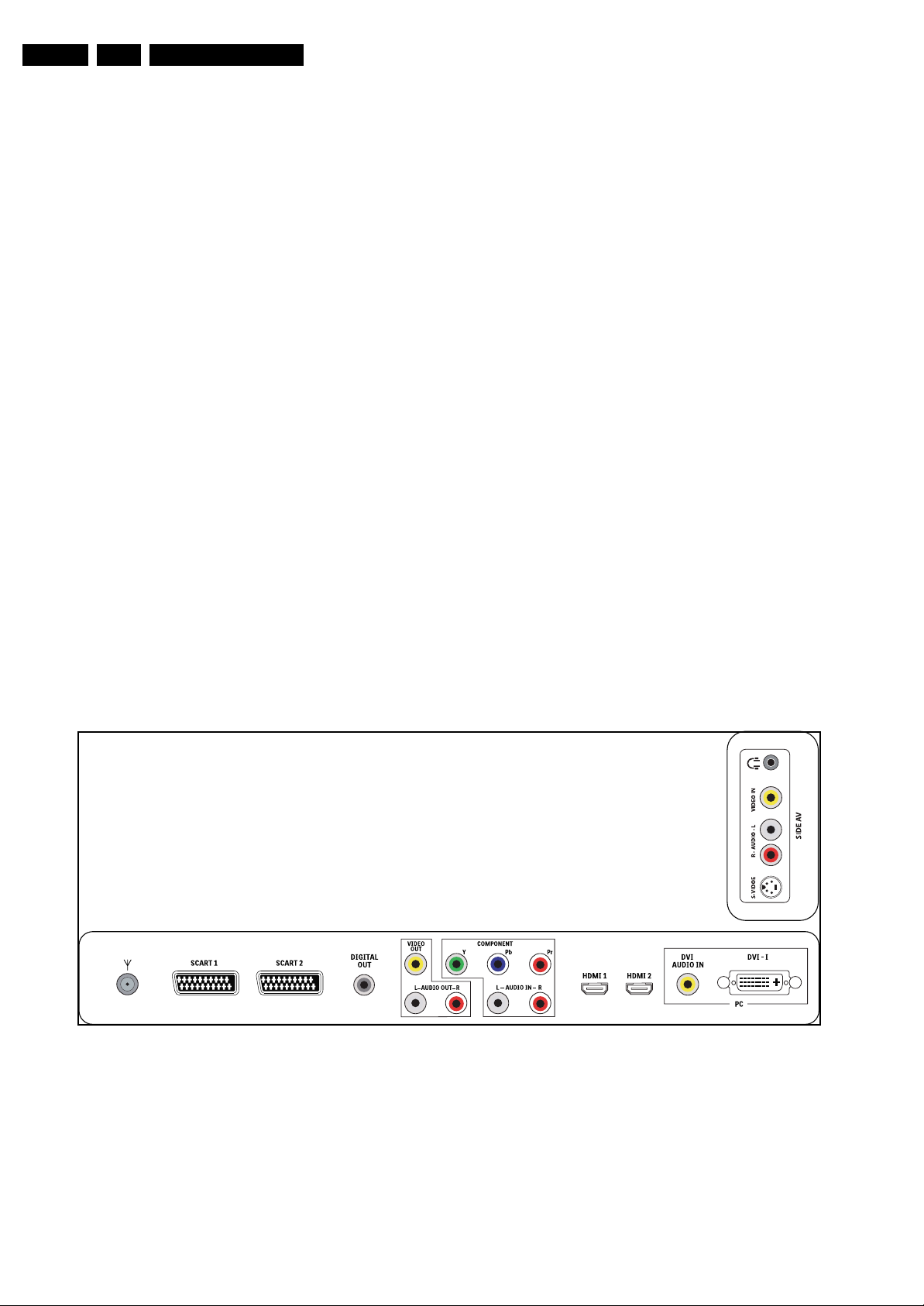
1.2 Connection Overview
Note: The following connector colour abbreviations are used
(acc. to DIN/IEC 757): Bk= Black, Bu= Blue, Gn= Green, Gy=
Grey, Rd= Red, Wh= White, and Ye= Yellow.
Figure 1-1 Connection overview
H_17490_010.eps
291007
1.2.1 Side Connections
Mini Jack: Audio Head phone - Out
Bk - Head phone 32 - 600 ohm / 10 mW ot
Cinch: Video CVBS - In, Audio - In
Ye - Video CVBS 1 V
Wh - Audio L 0.5 V
Rd - Audio R 0.5 V
/ 75 ohm jq
PP
/ 10 kohm jq
RMS
/ 10 kohm jq
RMS
S-Video (Hosiden): Video Y/C - In
1 -Ground Y Gnd H
2 -Ground C Gnd H
3 - Video Y 1 V
4 - Video C 0.3 V
/ 75 ohm j
PP
P / 75 ohm j
PP
Page 3
Technical Specifications, Connections, and Chassis Overview
EN 3TES2.0E LA 1.
1.2.2 Rear Connections
Aerial - In
- - IEC-type Coax, 75 ohm D
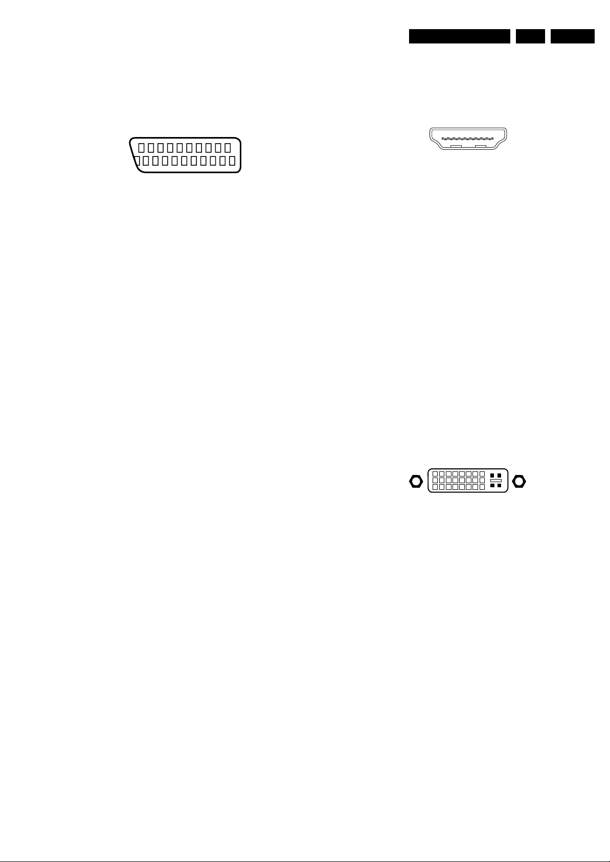
EXT1: AV + RGB
21
20
E_06532_001.eps
2
1
050404
Figure 1-2 SCART connector EXT1
1 - Audio R 0.5 V
2 - Audio R 0.5 V
3 - Audio L 0.5 V
4 - Ground Gnd (audio) H
/ 1 kohm k
RMS
/ 10 kohm j
RMS
/ 1 kohm k
RMS
5 - Ground Gnd H
6 - Audio L 0.5 V
7 - Video Blue 0.7 V
8 - Function Select 0 - 2 V: INT
/ 10 kohm j
RMS
/ 75 ohm j
PP
4.5 - 12 V: EXT 4:3 j
9 - Ground Gnd H
10 - Res. Clock signals
11 - Video Green 0.7 V
12 - Res. Remote control
/ 75 ohm j
PP
13 - Ground Gnd H
14 - Ground Gnd (switch RGB) H
15 - Video Red 0.7 V
16 - Switch RGB j
/ 75 ohm j
PP
17 - Ground Gnd (video) H
18 - Ground Gnd (video out) H
19 - Video out 1 V
20 - Video in 1 V
21 - Shield Gnd H
/ 75 ohm k
PP
/ 75 ohm j
PP
EXT2: AV + S-Video
1 - Audio R 0.5 V
2 - Audio R 0.5 V
3 - Audio L 0.5 V
/ 1 kohm k
RMS
/ 10 kohm j
RMS
/ 1 kohm k
RMS
4 - Ground Gnd (audio) H
5 - Ground Gnd H
6 - Audio L 0.5 V
7 - Video Blue 0.7 V
8 - Function Select 0 - 2 V: INT
/ 10 kohm j
RMS
/ 75 ohm j
PP
4.5 - 12 V: EXT 4:3 j
9 - Ground Gnd H
10 - Res. Clock signals
11 - Video Green 0.7 V
/ 75 ohm j
PP
12 - Res. Remote control
13 - Ground Gnd H
14 - Ground Gnd (switch RGB) H
15 - Video Red 0.7 V
16 - Switch RGB j
/ 75 ohm j
PP
17 - Ground Gnd (video) H
18 - Ground Gnd (video out) H
19 - Video out 1 V
20 - Video in 1 V
/ 75 ohm k
PP
/ 75 ohm j
PP
21 - Shield Gnd H
Cinch: S/PDIF - Out
Bk - Coaxial 0.4 - 0.6V
/ 75 ohm kq
PP
Cinch: Video CVBS - Out, Audio - Out
Ye - Video CVBS 1 V
Wh - Audio L 0.5 V
Rd - Audio R 0.5 V
/ 75 ohm kq
PP
/10 kohm kq
RMS
/ 10 kohm kq
RMS
Cinch: Video YPbPr - In, Audio - In
Gn - Video Y 1 V
/ 75 ohm jq
PP
Bu - Video Pb 0.7 V
Rd - Video Pr 0.7 V
Wh - Audio L 0.5 V
Rd - Audio R 0.5 V
/ 75 ohm jq
PP
/ 75 ohm jq
PP
/ 10 kohm jq
RMS
/ 10 kohm jq
RMS
HDMI: Digital Video, Digital Audio - In
19
18 2
1
E_06532_017.eps
250505
Figure 1-3 HDMI (type A) connector
1 - D2+ Data channel j
2 - Shield Gnd H
3 - D2- Data channel j
4 - D1+ Data channel j
5 - Shield Gnd H
6 - D1- Data channel j
7 - D0+ Data channel j
8 - Shield Gnd H
9 - D0- Data channel j
10 - CLK+ Data channel j
11 - Shield Gnd H
12 - CLK- Data channel j
13 - n.c.
14 - n.c.
15 - DDC_SCL DDC clock j
16 - DDC_SDA DDC data jk
17 - Ground Gnd H
18 - +5V j
19 - HPD Hot Plug Detect j
20 - Ground Gnd H
PC: Mini Jack: PC/DVI Audio - In
Wh - Audio L 0.5 V
Rd - Audio R 0.5 V
/ 10 kohm jq
RMS
/ 10 kohm jq
RMS
PC: DVI-I: Digital/Analogue Video - In
1 8
916
17
C1 C2
C5
24
C3 C4
E_06532_004.eps
050404
Figure 1-4 DVI-I connector
1-D2- j
2-D2+ j
3 - Shield Gnd H
4-D4- j
5-D4+ j
6 - DDC_SCL DDC clock k
7 - DDC_SDA DDC data jk
8 - V-sync 0 - 5 V j
9-D1- j
10 - D1+ j
11 - Shield Gnd H
12 - D3- j
13 - D3+ j
14 - +5V j
15 - Ground Gnd H
16 - HPD Hot Plug Detect j
17 - D0- j
18 - D0+ j
19 - Shield Gnd H
20 - D5- j
21 - D5+ j
22 - Shield Gnd H
23 - CLK+ j
24 - CLK- j
C1 - Video Red 0.7 V
C2 - Video Green 0.7 V
C3 - Video Blue 0.7 V
/ 75 ohm j
PP
/ 75 ohm j
PP
/ 75 ohm j
PP
C4 - H-sync 0 - 5 V j
Page 4
EN 4 TES2.0E LA1.
C5 - Ground Gnd H
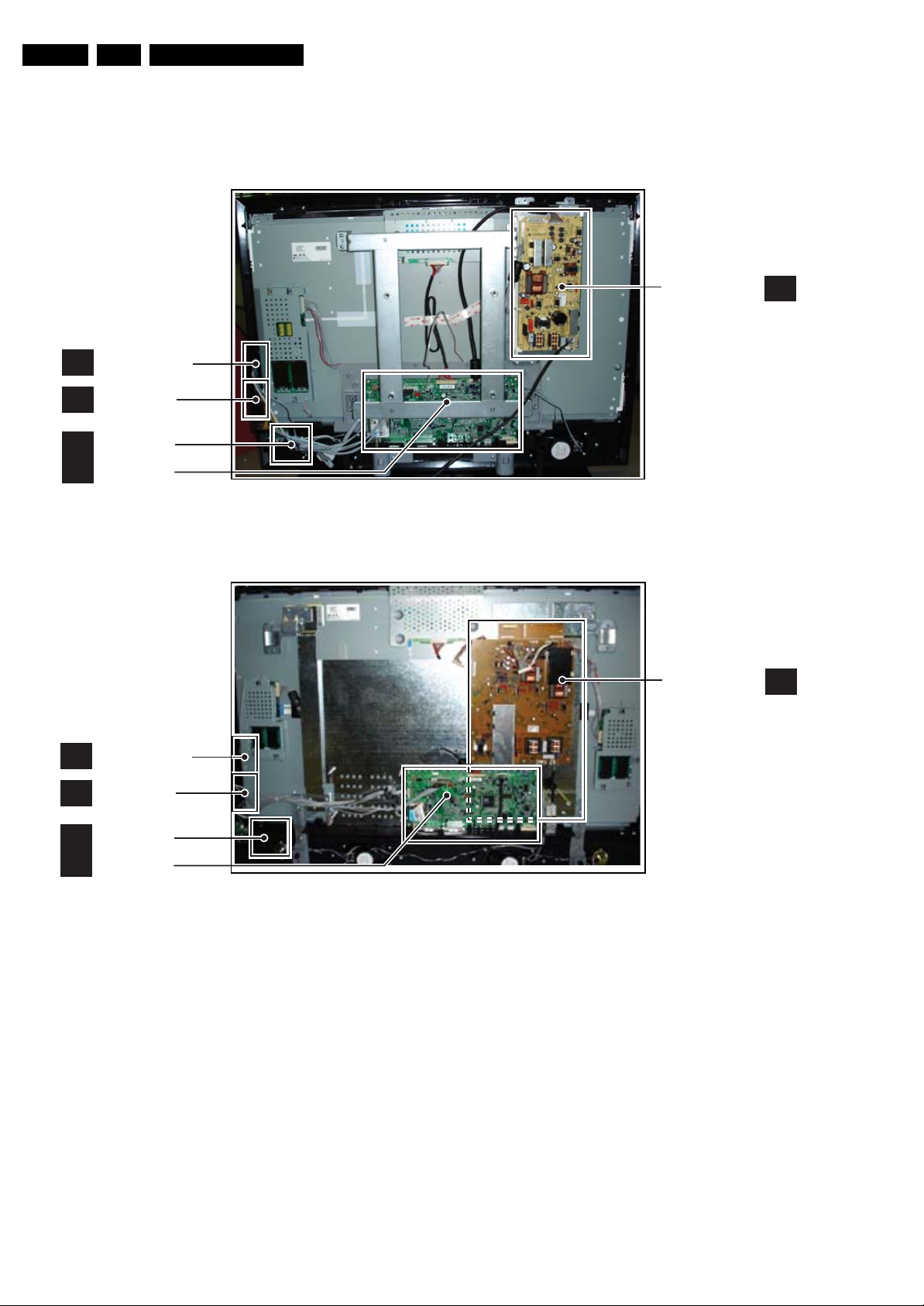
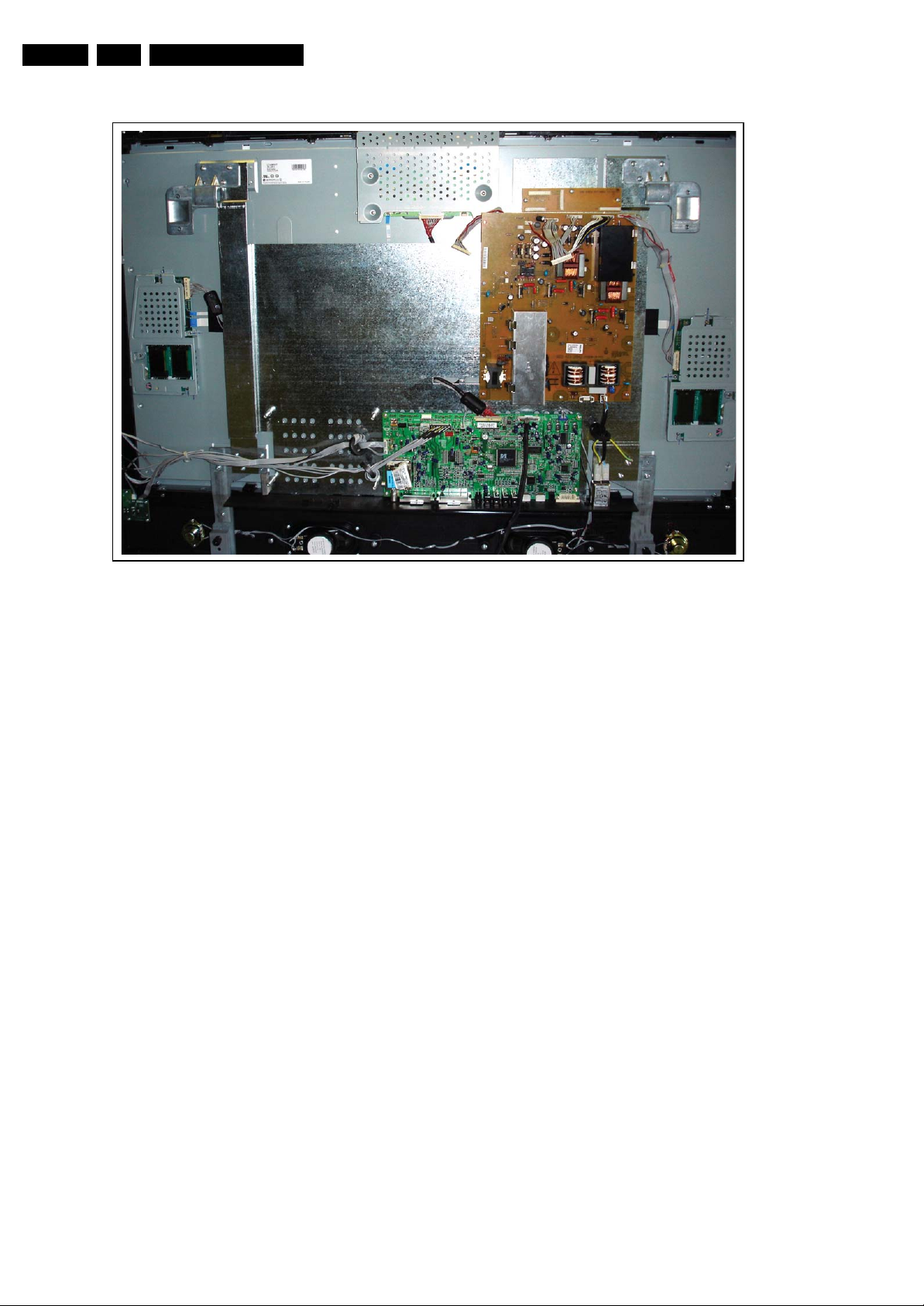
1.3 Chassis Overview
Technical Specifications, Connections, and Chassis Overview
CONTROL BOARD
E
SIDE I/O PANEL
D
LED PANEL
J
MAIN BOARD
B
(incl ext. I/O)
Figure 1-5 PWB locations 32"
H_17490_012.eps
291007
POWER SUPPLY
BOARD
POWER SUPPLY
BOARD
A
A
CONTROL BOARD
E
SIDE I/O PANEL
D
LED PANEL
J
MAIN BOARD
B
(incl ext. I/O)
Figure 1-6 PWB locations 42"
H_17490_014.eps
291007
Page 5

Safety Instructions, Warnings, and Notes
2. Safety Instructions, Warnings, and Notes
EN 5TES2.0E LA 2.
Index of this chapter:
2.1 Safety Instructions
2.2 Warnings
2.3 Notes
2.1 Safety Instructions
Safety regulations require the following during a repair:
• Connect the set to the Mains/AC Power via an isolation
transformer (> 800 VA).
• Replace safety components, indicated by the symbol h,
only by components identical to the original ones. Any
other component substitution (other than original type) may
increase risk of fire or electrical shock hazard.
Safety regulations require that after a repair, the set must be
returned in its original condition. Pay in particular attention to
the following points:
• Route the wire trees correctly and fix them with the
mounted cable clamps.
• Check the insulation of the Mains/AC Power lead for
external damage.
• Check the strain relief of the Mains/AC Power cord for
proper function.
• Check the electrical DC resistance between the Mains/AC
Power plug and the secondary side (only for sets that have
a Mains/AC Power isolated power supply):
1. Unplug the Mains/AC Power cord and connect a wire
between the two pins of the Mains/AC Power plug.
2. Set the Mains/AC Power switch to the “on” position
(keep the Mains/AC Power cord unplugged!).
3. Measure the resistance value between the pins of the
Mains/AC Power plug and the metal shielding of the
tuner or the aerial connection on the set. The reading
should be between 4.5 Mohm and 12 Mohm.
4. Switch “off” the set, and remove the wire between the
two pins of the Mains/AC Power plug.
• Check the cabinet for defects, to prevent touching of any
inner parts by the customer.
2.2 Warnings
• All ICs and many other semiconductors are susceptible to
electrostatic discharges (ESD w). Careless handling
during repair can reduce life drastically. Make sure that,
during repair, you are connected with the same potential as
the mass of the set by a wristband with resistance. Keep
components and tools also at this same potential.
• Be careful during measurements in the high voltage
section.
• Never replace modules or other components while the unit
is switched “on”.
• When you align the set, use plastic rather than metal tools.
This will prevent any short circuits and the danger of a
circuit becoming unstable.
2.3 Notes
2.3.1 General
• Measure the voltages and waveforms with regard to the
chassis (= tuner) ground (H), or hot ground (I), depending
on the tested area of circuitry. The voltages and waveforms
shown in the diagrams are indicative. Measure them in the
Service Default Mode (see chapter 5) with a colour bar
signal and stereo sound (L: 3 kHz, R: 1 kHz unless stated
otherwise) and picture carrier at 475.25 MHz for PAL, or
61.25 MHz for NTSC (channel 3).
• Where necessary, measure the waveforms and voltages
with (D) and without (E) aerial signal. Measure the
voltages in the power supply section both in normal
operation (G) and in stand-by (F). These values are
indicated by means of the appropriate symbols.
• Manufactured under license from Dolby Laboratories.
“Dolby”, “Pro Logic” and the “double-D symbol”, are
trademarks of Dolby Laboratories.
2.3.2 Schematic Notes
• All resistor values are in ohms, and the value multiplier is
often used to indicate the decimal point location (e.g. 2K2
indicates 2.2 kohm).
• Resistor values with no multiplier may be indicated with
either an “E” or an “R” (e.g. 220E or 220R indicates 220
ohm).
• All capacitor values are given in micro-farads (μ= × 10
nano-farads (n= × 10
• Capacitor values may also use the value multiplier as the
decimal point indication (e.g. 2p2 indicates 2.2 pF).
• An “asterisk” (*) indicates component usage varies. Refer
to the diversity tables for the correct values.
• The correct component values are listed in the Spare Parts
List. Therefore, always check this list when there is any
doubt.
2.3.3 BGA (Ball Grid Array) ICs
Introduction
For more information on how to handle BGA devices, visit this
URL: www.atyourservice.ce.philips.com (needs subscription,
not available for all regions). After login, select “Magazine”,
then go to “Repair downloads”. Here you will find Information
on how to deal with BGA-ICs.
BGA Temperature Profiles
For BGA-ICs, you must use the correct temperature-profile,
which is coupled to the 12NC. For an overview of these profiles,
visit the website www.atyourservice.ce.philips.com (needs
subscription, but is not available for all regions)
You will find this and more technical information within the
“Magazine”, chapter “Repair downloads”.
For additional questions please contact your local repair help
desk.
2.3.4 Lead-free Soldering
Due to lead-free technology some rules have to be respected
by the workshop during a repair:
• Use only lead-free soldering tin Philips SAC305 with order
code 0622 149 00106. If lead-free solder paste is required,
please contact the manufacturer of your soldering
equipment. In general, use of solder paste within
workshops should be avoided because paste is not easy to
store and to handle.
• Use only adequate solder tools applicable for lead-free
soldering tin. The solder tool must be able:
– To reach a solder-tip temperature of at least 400°C.
– To stabilize the adjusted temperature at the solder-tip.
– To exchange solder-tips for different applications.
• Adjust your solder tool so that a temperature of around
360°C - 380°C is reached and stabilized at the solder joint.
Heating time of the solder-joint should not exceed ~ 4 sec.
Avoid temperatures above 400°C, otherwise wear-out of
tips will increase drastically and flux-fluid will be destroyed.
To avoid wear-out of tips, switch “off” unused equipment or
reduce heat.
• Mix of lead-free soldering tin/parts with leaded soldering
tin/parts is possible but PHILIPS recommends strongly to
-9
), or pico-farads (p= × 10
-12
-6
),
).
Page 6

EN 6 TES2.0E LA3.
Directions for Use
avoid mixed regimes. If this cannot be avoided, carefully
clear the solder-joint from old tin and re-solder with new tin.
2.3.5 Alternative BOM identification
The third digit in the serial number (example:
AG2B0335000001) indicates the number of the alternative
B.O.M. (Bill Of Materials) that has been used for producing the
specific TV set. In general, it is possible that the same TV
model on the market is produced with e.g. two different types
of displays, coming from two different suppliers. This will then
result in sets which have the same CTN (Commercial Type
Number; e.g. 28PW9515/12) but which have a different B.O.M.
number.
By looking at the third digit of the serial number, one can
identify which B.O.M. is used for the TV set he is working with.
If the third digit of the serial number contains the number “1”
(example: AG1B033500001), then the TV set has been
manufactured according to B.O.M. number 1. If the third digit is
a “2” (example: AG2B0335000001), then the set has been
produced according to B.O.M. no. 2. This is important for
ordering the correct spare parts!
For the third digit, the numbers 1...9 and the characters A...Z
can be used, so in total: 9 plus 26= 35 different B.O.M.s can be
indicated by the third digit of the serial number.
Identification: The bottom line of a type plate gives a 14-digit
serial number. Digits 1 and 2 refer to the production center (e.g.
AG is Bruges), digit 3 refers to the B.O.M. code, digit 4 refers
to the Service version change code, digits 5 and 6 refer to the
production year, and digits 7 and 8 refer to production week (in
example below it is 2006 week 17). The 6 last digits contain the
serial number.
3. Directions for Use
You can download this information from the following websites:
http://www.philips.com/support
http://www.p4c.philips.com
MODEL :
PROD.NO:
2.3.6 Board Level Repair (BLR) or Component Level Repair (CLR)
If a board is defective, consult your repair procedure to decide
if the board has to be exchanged or if it should be repaired on
component level.
If your repair procedure says the board should be exchanged
completely, do not solder on the defective board. Otherwise, it
cannot be returned to the O.E.M. supplier for back charging!
2.3.7 Practical Service Precautions
• It makes sense to avoid exposure to electrical shock.
• Always respect voltages. While some may not be
32PF9968/10
AG 1A0617 000001
Figure 2-1 Serial number (example)
While some sources are expected to have a possible
dangerous impact, others of quite high potential are of
limited current and are sometimes held in less regard.
dangerous in themselves, they can cause unexpected
reactions that are best avoided. Before reaching into a
powered TV set, it is best to test the high voltage insulation.
It is easy to do, and is a good service precaution.
MADE IN BELGIUM
220-240V 50/60Hz
~
VHF+S+H+UHF
BJ3.0E LA
S
E_06532_024.eps
128W
130606
Page 7
4. Mechanical Instructions
Index of this chapter:
4.1 Cable Dressing
4.2 Set Dis-assembly
4.3 Set Re-assembly
4.1 Cable Dressing
Mechanical Instructions
Notes:
• Figures below can deviate slightly from the actual situation,
due to the different set executions.
EN 7TES2.0E LA 4.
Figure 4-1 Cable Dressing 32" sets
H_17490_011.eps
291007
Page 8
EN 8 TES2.0E LA4.
Mechanical Instructions
4.2 Set Dis-assembly
Following figures (“exploded view”) indicate the mechanical
construction of the sets.
Figure 4-2 Cable Dressing 42" sets
H_17490_013.eps
291007
Page 9

Mechanical Instructions
EN 9TES2.0E LA 4.
291007
H_17490_015.eps
Figure 4-3 Exploded View 32" sets
Page 10

EN 10 TES2.0E LA4.
Mechanical Instructions
291007
H_17490_016.eps
Figure 4-4 Exploded View 42" sets
Page 11

4.3 Set Re-assembly
Note:
While re-assembling, make sure that all cables are placed and
connected in their original position. See figures “Cable
dressing”.
Mechanical Instructions
EN 11TES2.0E LA 4.
Page 12
EN 12 TES2.0E LA5.
Service Modes, Error Codes, and Fault Finding
5. Service Modes, Error Codes, and Fault Finding
Index of this chapter:
5.1 Service Mode
5.2 Error Codes
5.3 Fault Finding and Repair Tips
5.1 Service Mode
The Service Mode is activated by pressing ‘1923’ on the
Remote Control, while the set is in the Main User Menu.
The software provides menu flexibility and full control to the
software. Service persons can adjust the TV in all manners. In
the Service Menu (see chapter 8), you find a list of parameters.
All functions of the Service Mode, and the default parameter
settings, are listed in Chapter “Alignments”.
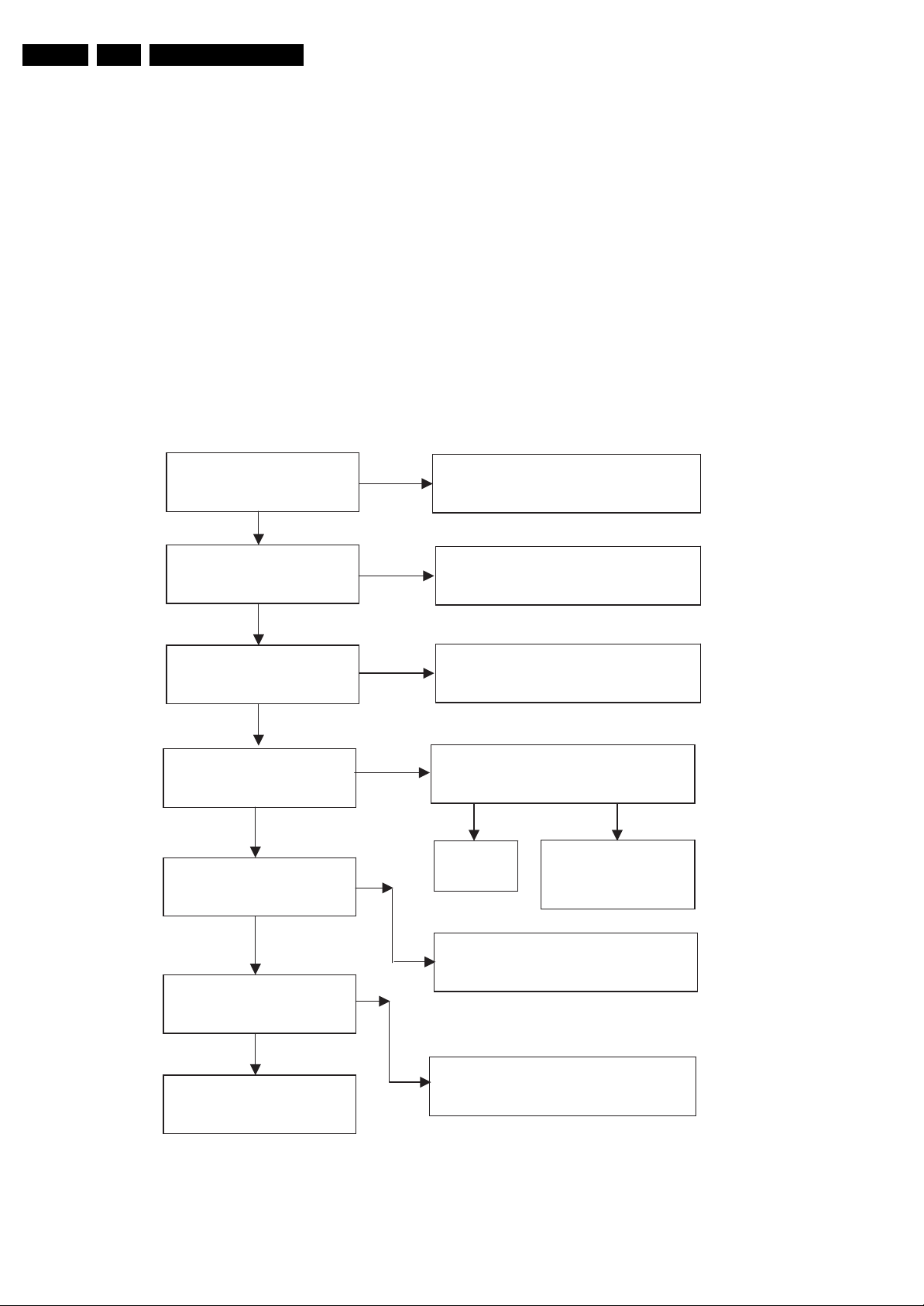
FAULT TRACING DIAGRAM FOR POWER SUPPLY
Check 220 V AC Mains
YES
Check C 020 Voltage
NO
NO
5.2 Error Codes
These sets do not generate Error Codes.
5.3 Fault Finding and Repair Tips
Notes:
• It is assumed that the components are mounted correctly
with correct values and no bad solder joints.
• Before any fault finding actions, check if the correct options
are set.
• The Service Menu (see chapter 8), contains some useful
tests, that generates patterns.
Check AC Power Cable is Plugged
Check X102 Fuse
YES
Check 5VSTBY
YES
Check 5V_OFF
YES
Check 24V,33V,12V
8V
YES
Check 3.3V,2.5V and 1.8V
YES
NO
NO
NO
NO
Check T530 and Peripheral
Components
Check P_CTRL Pin
LOW HIGH
StandBy
Mode
Normal Mode
Check Components
For 5V
Check Related Components for
Defective Outputs
POWER IS OK
Check Related Components
Figure 5-1 Fault finding power supply
H_17490_017.eps
291007
Page 13

Block Diagrams, Test Point Overviews, and Waveforms
6. Block Diagrams, Test Point Overviews, and Waveforms
Block Diagram Main
EN 13TES2.0E LA 6.
H_17490_018.eps
291007
Page 14

Block Diagrams, Test Point Overviews, and Waveforms
Block Diagram ASSOS Chassis
220 V AC
POWER BOARD
EN 14TES2.0E LA 6.
IDTV CHASSIS DIAGRAM
24 V
S300
CN16
CN15
CN17
CN19
*
*
*
*
5V
5V STD
12V
STD BY
Back light On/Off
Back light Dimm
CN7
MAIN BOARD ASSOS
CN20 CN21
CN5
Speaker
CN4
CN18
LVDS
J7
Dyn. Cont.
CN24
24 V
Back light Dimm
LCD
PANEL
Back light On/Off
*
Service
IR
MULTI
BUTTON
CN15-16-17-19 are for optional DVB connections
SIDE
AV
H_17490_019.eps
291007
Page 15

Block Diagrams, Test Point Overviews, and Waveforms
Block Diagram Board Location
EN 15TES2.0E LA 6.
CN12
CN20
CN21
CN15
CN11
CN13
CN17
CN16
CN9 CN8
CN18 (CN22)
CN19
J7
J10
CN7
CN4
CN5
TUNER
SCART1 SCART2
SPDIF
OUT
LINE OUT
COMPONENT INPUT
HDMI1
HDMI2
PC
SOUND
DVI
H_17490_020.eps
291007
Page 16

Circuit Diagrams and PWB Layouts
7. Circuit Diagrams and PWB Layouts
Power Supply Panel
1
POWER SUPPLY PANEL
A A
D
C
B
A
12
S303
POWER
2
HS33
SMPS HEATSINK
1
TP56
2
1
F300
T3.15AL/250V
2
TP57
C308
100nF 275VAC
HS34
SMPS HEATSINK
1
TP58
VR30
V320
3
2
1
23
L800
2X27mH
R300
8.2K
100nF 275VAC
L310
4
23
C357
TP59
1
TP60
2X27mH
J304
TP130
R400
C400
8.2K
10pF
J317
3
TP1
R301
56K
IC30
1
NC
2
PCS
3
RZI
TP2
4
SRC
TP3
4
TP131
100nF 275VAC
R402
56K
J302
ICE1QS01
TP4
C302
330pF
TP61
C337
TP62
IC40
1
NC
2
PCS
TP132
3
RZI
SRC4OFC
ICE1QS01
R403
J316
1M
TP133
C403
330pF
C301
C300
47nF
10pF
C401
100nF
EN 16TES2.0E LA 7.
TP26
D302
MBR20200CT
TP27
T301
BC848B
TP73
TP116
MBR20200CT
TP141
T400
BC848B
F301
TP29
5VSTBY
TP74
TP75
STPS5L40
TP117
R201
1K
TP118
D404
5VOC
D320
5.1V
TP142
76
R308
100R
R309
100R
5A
D305
MBR1045
TP78
D304
BAT85
TP79
R344
47R
TP76
R314
1K
R315
470R
J308
R317
1K
TP77
R326
1K
D200
C210
470uF/35V
R202
470R
D202
TL431
R412
10R
TP119
R413
10R
TP144
R416
1K
R417
470R
D403
TL431
R414
1K
TP143 TP147
R415
1K
TP35
5VMAIN
TP80
J310 J318J306
TP145
TP37
C305
220pF
TP30
C303
220pF
R320
100R
D310
MBR1045
D306
BAT85
R345
47R
C359
100nF
D303
TL431
TP81
TP82
C204
100nF
C207
47pF
TP120
TP121
TP146
C408
100nF
STB
J328 J326
TP34 TP38
C314
C329
100nF
2200uF/25V
TP31TP28
C336
220pF
1000uF/16V
TP32
R310
C330
12K
C343
10uF
TP83TP72
C342
47pF
TP85
R321
33K
STB
R346
3.3K
TP84 TP86
T302
BC848B
R203
1K
L200
J320
20uH 2.5A
C211
470uF/16V
TP122
C208
R200
15nF
2.4K 1%
TP123
R205
33K
TP126
R337
2.4K 1%
C416
1nF 1KV
TP124
C417
1nF 1KV
C414
2200uF/35V
C421
10uF
J323
C418
C419
47pF
15nF
R418
33K
TP148
J325
54
R304
R305
150K
150K
Q300
TP10
BC337
J315
TP7
10uF/25V
C356
C317
100nF
D318
C345
33pF
8
VCC
7
OUT
TP6
6
GND
TP8
J307
5
OFC
R302
1M
3
4
TP5
L311
PFC
1
6
TP63
TP100
C304
22pF
8
VCC
7
OUT
TP134
6
GND
TP135
5
2.4V
TP11
D315
12V
R306
100R
D300
R307
33R
TP9
1N4148
C306
10pF
TP12
C320
1nF/1KV
4
C321
1nF/1KV
23
TP64
R332
R316
150K
150K
TP101 TP111
10uF/25V
C360
C335
100nF
D319
2.4V
TP102
D317
12V
R404
100R
D400
R405
33R
TP137
TP136
1N4148
TP18
R333
TP19
4.7K
TP14
TP15
R339
4.7K
Q302
BC848B
23
1
TP13
TP16
J313
C318
IC36
1nF/1KV
C319
RS406
1nF/1KV
Q301
BC337
TP103
TP104
Q303
BC848B
23
1
C307
10pF
T300
SPP07N60
TP17
1
TP65
TP105
R334
4.7K
R340
TP109
T401
SPP07N60
33nF/630V
J303
R319
D325
1.2M
1N4007
J300
J301
D326
1N4007
R343
1.2M
4.7K
L305
BEAD
L306
BEAD
C411
TP20
R341
270R
TP21
L304
BEAD
L301
BEAD
TP22
TP23
TP66
100uF/400V
VB3
TP107
TP108
R342
270R
TP139 TP140
D321
33V
D322
12V
D308
BYW76
R329
68K 1W
VB
C324
270uF/400V
TP110
7
8
D
VST
GND1GND2GND3VFB
C362
D323
33V
D324
8.2V
D402
BYW76
TP138
R410
68K 1W
C404
8.2nF 400V
C341
33nF 630V
R204
68K 1W
5
VCC
4
C413
680pF 2000V
C322
47uF/50V
IC21
FSD200
C203
100nF
47uF/50V
D301
BYV36C
L302
BEAD
C325
680pF 2000V
L303
BEAD
C328
8.2nF 400V
2.2nF 400VAC
TP112
TP113
C410
L400
BEAD
L401
BEAD
D401
BYV36C
C202
D201
BYV36C
C213
33uF
J319Comment
J305
J311
TP24
J314
TP25
VB2
C361
8.2nF 400V
TP114TP106
TP115
C402
8.2nF 400V
J312
TP67
TP68
TR30
6
5
3
1
SMPS LCD MAIN
IC37
6
5
4
1nF 400VAC
1nF 400VAC
TP69 TP71
2.2nF 400VAC
TR20
4
1
SMPS STANDBY LCD
IC20
6
5
4
TCDT1101G
TR40
3
4
1
6
SMPS LCD BL
IC41
6
5
4
TCDT1101G
6
5
TCDT1101G
R303
4.7M 1/2W
C206
1nF 400VAC
6
5
4
6
5
15
13
16
13
14
12
9
11
10
11
5VOC
1
1
2
2
334
C338
TP70
C339
C340
GND
6
10
1
1
2
2
3
3
11
7
12
8
1
1
2
2
334
4567
1000uF 16V
C344
15nF
J322
STDBY
R347
33K
5VSTBY
TP125
R419
30K 1%
L307
20uH 2.5A
C948
TP87
100nF
C200
47nF
8
12V
R327
2.2K
C334
1000uF/16V
C347
100nF
5VMAIN
C316
100nF
1
FD1 FD2 FD3
J324
C332
1000uF/25V
J309
OPS.
TP41
C312
100nF
HS30
2
POWER HEATSINK
1
C354
C351
1000uF/25V
100nF/50V
L308
10uH 7A
TP36
C315
100nF
TP88
R322
5.6K 1%
TP89
R330
22K 1%
C205
R331
C358
4.7K 1%
47nF
R336
1K 1%
109
HS32
POWER HEATSINK
2
HS35
POWER HEATSINK
1
2
1
2
5VMAIN
5VSTBY
STDBY
TP43
12V
A_DIM
BL_ON/OFF
J330
12V
5VMAIN
TP50
J331
J329
BL_ON/OFF
11
S300
1
2
3
4
5
6
7
8
9
10
11
12
POWER
24V
1
TP53
2
3
4
5
BGND
6
7
TP92
8
9
10
11
TP93
12
13
14
A_DIM
TP95
4
3
2
1
24V
S305
TP55
TP96
TP97
TP98
TP99
CON14
S301
CON4
12
D
S302
1
2
3
4
5
6
7
8
9
10
CON10_W
C
B
5VOC
TP127
D309
1N4148
TP128
R335
24V
2.7K
L402
10uH 7A
C405
100nF
TP129
470uF/35V
J327
C420
C406
100nF
24V
TP149
C409
47nF
R338
3.4K 1%
H_17490_021.eps
8
910
2111
A
161007
Page 17

Circuit Diagrams and PWB Layouts
EN 17TES2.0E LA 7.
Layout Power Supply Panel (Top Side)
Layout Power Supply Panel (Top Side)
H_17490_022.eps
161007
H_17490_023.eps
161007
Page 18

Circuit Diagrams and PWB Layouts
EN 18TES2.0E LA 7.
Main Board: HDMI & DVI-I Input
5
4
3
2
1
HDMI & DVI-I INPUT
CN14
SHELL1
NC1
DATA2DATA2+
DATA2/4_SHLD
DATA4DATA4+
DDC_CLK
DDC_DATA
A_VSYNC
DATA1DATA1+
DATA1/3_SHLD
DATA3-
DATA3+
H_PLUG_DET
DATA0DATA0+
DATA0/5_SHLD
DATA5DATA5+
CLK_SHLD
A_RED
A_GREEN
A_BLUE
A_HSYNC
A_GND1
A_GND2
NC2
SHELL2
DVI_AD_CON
GND
CLK+
CLK-
VSS5
32
1
2
3
4
5
6
7
8
9
10
11
12
13
14
+5V
15
16
17
18
19
20
21
22
23
24
25
26
27
28
29
30
31
B1 B1
D D
C C
33
34
HDMI 1
GND
202122
23
J2
T1T2T3
T4
19
HPDET
18
+5V
17
CEC/GND
16
SDA
15
SCL
14
NC
13
CEC
12
CLK-
11
CLKS
10
CLK+
9
DATA0-
8
DATA0S
7
DATA0+
6
DATA1-
5
DATA1S
4
DATA1+
3
DATA2-
2
DATA2S
1
DATA2+
HDMI_CONN_RA
B B
R561 0R
HDMI2HDMI1
VSS5
HDMI2
GND
202122
23
J3
T1T2T3
T4
19
HPDET
18
+5V
17
CEC/GND
16
SDA
15
SCL
14
NC
13
CEC
12
CLK-
11
CLKS
10
CLK+
9
DATA0-
8
DATA0S
7
DATA0+
6
DATA1-
5
DATA1S
4
DATA1+
3
DATA2-
2
DATA2S
1
A A
DATA2+
HDMI_CONN_RA
VSS5
HDMI1
D11
BAV70
2
1
D2
BAV70
2
1
C24
10uF_2012
R20 1K
D3
BAV70
2
1
C27
10uF_2012
R341K
HDMI2
R466
1K
3
R468
R467
C376
C377
10uF_2012
100nF
3
3
C28
100nF
10K
R475 100
R476 100
R15
47K
C25
100nF
R30
47K
10K
R469 0R
12
R470 0R
12
R471 100
R472 100
R16
47K
R17 0R
R19 0R
C43 22pF(NU)
C44 22pF(NU)
R31
47K
R320R
R33 0R
C47 22pF(NU)
C48 22pF(NU)
U29
6 8
SCL VCC
5
SDA
1
A0
2
A1
3
A2
24C02
DVI_RX2DVI_RX2+
C448 22pF(NU)
C449 22pF(NU)
DVI_DDC_CLK
DVI_DDC_DATA
DVI_RX1DVI_RX1+
DVI_HPD
DVI_RX0DVI_RX0+
DVI_RXC+
DVI_RXC-
HS_MST4
VS_MST4
232_RXD 8
232_TXD 8
U4
6 8
SCL VCC
5
SDA
1
A0
A1
A2
24C02
U5
SCL VCC
SDA
A0
A1
A2
GND
24C02
HDMI_DDC_DATA_2
HDMI_DDC_CLK_2
WP
GND
HDMI1_HPD
HDMI_DDC_DATA_1
HDMI_DDC_CLK_1
WP
HDMI2_HPD
HDMI_RXC-_2
HDMI_RXC+_2
HDMI_RX0-_2
HDMI_RX0+_2
HDMI_RX1-_2
HDMI_RX1+_2
HDMI_RX2-_2
HDMI_RX2+_2
2
3
6 8
5
1
2
3
7
WP
4
GND
7
4
HDMI_RXC-_1
HDMI_RXC+_1
HDMI_RX0-_1
HDMI_RX0+_1
HDMI_RX1-_1
HDMI_RX1+_1
HDMI_RX2-_1
HDMI_RX2+_1
7
4
C29
100nF
C378
100nF
C379
10pF
C380
10pF
C381
10pF
C26
100nF
12
R473
75_1%
12
R474
75_1%
12
R477
75_1%
VGA_B 4
DVI_HPD
MMBT3904
HDMI2_HPD
MMBT3904
HDMI1_HPD
MMBT3904
VGA_R 4
VGA_G 4
Q30
Q31
Q32
J1
PHONE_JACK
PC_L
R1
R2
GND
PC_R
R564 5.1K(NU)
32
1
R565 5.1K(NU)
32
1
R566 5.1K(NU)
32
1
3
L1
4
L2
2
5
1
DVI_RX2+
DVI_RX2DVI_RX1+
DVI_RX1DVI_RX0+
DVI_RX0DVI_RXC+
DVI_RXC-
HDMI_RX2+_2
HDMI_RX2-_2
HDMI_RX1+_2
HDMI_RX1-_2
HDMI_RX0+_2
HDMI_RX0-_2
HDMI_RXC+_2
HDMI_RXC-_2
HDMI_RX2+_1
HDMI_RX2-_1
HDMI_RX1+_1
HDMI_RX1-_1
HDMI_RX0+_1
HDMI_RX0-_1
HDMI_RXC+_1
HDMI_RXC-_1
HPD1
HPD2
HPD3
DVI_DDC_CLK
DVI_DDC_DATA
HDMI_DDC_CLK_2
HDMI_DDC_DATA_2
HDMI_DDC_CLK_1
HDMI_DDC_DATA_1
ED3
BAV99(NU)
R567 15K
R568 15K
R569
0
R570
0
R571
0
2
3
HPD1
HPD2
HPD3
ED4
1
BAV99(NU)
HDMI_MUX
VSS_M3V :
190mA
U3
15
A14
14
B14
12
A13
11
B13
9
A12
8
B12
6
A11
5
B11
77
A24
76
B24
74
A23
73
B23
71
A22
70
B22
68
A21
67
B21
58
A34
57
B34
55
A33
54
B33
52
A32
51
B32
49
A31
48
B31
80
HPD1
62
HPD2
44
HPD3
3
SCL1
2
SDA1
64
SCL2
63
SDA2
46
SCL3
45
SDA3
2
1
3
NC
NC
20161
ED1
BAV99(NU)
1
12
12
NC
NC
41
60
3
R6
220K
R8
220K
7
VCC
2
13
VCC
VSS_M3V
17
27
VCC
GND
4
10
ED2
BAV99(NU)
3
2
1
C5
1nF
C6
1nF
33
43
50
VCC
VCC
VCC
TMDS341A
GND
GND
GND
24
30
VCC
GND
56
VCC
GND
36
69
61
VCC
VCC
GND
GND
37
47
PC/DVI_L_IN 8
PC/DVI_R_IN 8
79
75
VCC
VCC
GND
GND
GND
GND
53
59
66
65
S5VESD5V
U1
AP1117_3.3V-SOT223(NU)
3
VSS_M3V
12
C8
+
100nF
Output
de-emphass.
(VSADJ)
high : 3dB
low : 0dB
HDMI_RX2+ 4
HDMI_RX2- 4
HDMI_RX1+ 4
HDMI_RX1- 4
HDMI_RX0+ 4
HDMI_RX0- 4
HDMI_RXC+ 4
HDMI_RXC- 4
HDMI_DDC_DATA 4
HDMI_DDC_CLK 4
R456 100K
R28 0R(NU)
Q1
1
MMBT3904
VI
C1
100nF(NU)
VS_3V
FB1
600 Ohm 0.5A 2012(NU)
C7
100uF/16V
VSS_M3VA3.3V
FB63
600 Ohm 0.5A 2012
VSS_M3V
R18 4.64K_1%
18
VSADJ
19
PRE
25
Y4
26
Z4
28
Y3
29
Z3
31
Y2
32
Z2
34
Y1
35
Z1
39
SDA_SINK
38
SCL_SINK
40
HPD_SINK
21
S1
22
S2
23
S3
42
OE
GND
GND
78
72
R27
32
0R
2
VO
4
TAB
GND
1
100uF/16V(NU)
C10
C11
C9
10nF
10nF
10nF
R14 0RR13 10K
TMDS MUX OPTION(R18)
TI 4.64K(F grade)
PARADE 4.11K(F grade)
VSS_M3V
R454 47K(NU)
R455 47K(NU)
VSS_M3V
HPD_SINK 4
C3
C12
10nF
VSS_M3V
R21 4.7K(NU)
R22 4.7K(NU)
R23 4.7K(NU)
+
12
C13
10nF
VS_3V
C4
100nF(NU)
C14
10nF
DVI_ SEL 4
HDMI2_SEL 4
HDMI1_SEL 4
C15
10nF
C16
10nF
C17
10nF
C18
10nF
C19
10nF
H_17490_001.eps
5
4
3
2
1
161007
Page 19

Circuit Diagrams and PWB Layouts
EN 19TES2.0E LA 7.
Main Board: DVD & DTT Input
5
E
SD5V
2
3
1
3
2
1
BAV99(NU)
5VD
5VD
ED14
ED9
BAV99
R405
3.6K
R407
4.7K
R414
3.6K
R416
4.7K
ED6
BAV99
2
1
3
1
2
3
3
2
ED11
BAV99(NU)
1
1
R406
R410
MMBT3904
R415
R419
MMBT3904
2
BAV99
1
3
2
1
ED12
BAV99(NU)
3
2
82
82
1
Q25
82
82
1
Q27
ED8
BAV99
ESD5V
ED13
BAV99(NU)
C41
1nF
C42
1nF
AV_OUT 5
2
ED5
BAV99
1
3
B2
DVD & DTT INPUT
J4B UJB-04-13A
5
D D
C C
B B
3
J5A UJB-04-13A
3
J5B UJB-04-13A
3
J5C UJB-04-13A
6
J5D UJB-04-13A
6
J4A UJB-04-13A
3
J4C UJB-04-13A
6
J4D UJB-04-13A
6
2
C35
10pF
5
C40
10pF
1
4
BAV99
C50
+
220uF/16V
2
1
4
C32
10pF
R572
15K
R575
15K
A9V
ED15
M_L_OUT8
LINE_OUT_LA4
AV_OUT_L
AV_OUT_R
12
2
1
3
12
R37
75_1%
R40
75_1%
12
R41
75_1%
12
R45
220K
12
R46
220K
R53 75R
R428 0R ED68
R429 0R(NU)
PIP OPTION.
PIP OPTION.
M_R_OUT8
LINE_OUT_RA4
A A
R4300R
R431 0R(NU)
ED7
3
ED10
BAV99
3
2
1
MMBT3904
32
MMBT3904
32
1
Q24
R412
270
1
Q26
R421
270
4
MST_Y 4
MST_Pb/Cb 4
MST_Pr/Cr 4
DVD_L_IN 8
DVD_R_IN 8
32
R409
270
R411
470
32
R418
270
R420
470
HH1
MTHOLE
R408
470
1
2
C347
10uF_2012
1
2
R417
470
1
2
C350
10uF_2012
1
2
1
2
3
4
5
6
7
8
9
FM1
FM5
C346
10uF_2012
ED61
BAV99
ED63
BAV99
C349
10uF_2012
ED65
BAV99
ED67
BAV99
FM2
FM6
HH2
MTHOLE
FM3
FM7
1
3
1
3
1
3
1
3
FM4
FM8
3
3
3
3
3
HH4
HH3
1
2
3
4
5
6
7
8
9
MTHOLE
FM9
FM10
ED60
BAV99
2
ESD5V
ED62
BAV99
ESD5V
2
ED64
BAV99
2
ESD5V
ED66
BAV99
ESD5V
2
1
2
3
4
5
6
7
8
9
R413
1M
R422
1M
FM11
MTHOLE
FM12
C348
1nF
C351
1nF
1
2
3
4
5
6
7
8
9
HH5
HH6
12
R42 0R
R43 0R
R573
0(NU)
R574
0(NU)
VSS5
R484 470R(NU)
32
Q29
1
KSC1623
C452 10uF_2012
C453 10uF_2012
C454 10uF_2012
C455 10uF_2012
SPDIF_OPT
R482
4.7K
HS_L_OUT 5
AV_OUT_L
HS_R_OUT 5
AV_OUT_R
HDMI_SPDIF_OUT4
D_IR6
SVHS_YS8
SVHS_YD
SVHS_CS8
SVHS_CD
DVB_ SPDIF
R4810R
IR_MUTE4
R486 3.3K
SVHS_CS
C382 56pF
3
BAV99
R35
0R(NU)
R573, R574
Analog Tuner
only option.
1
2
2
2
3
5
6
11
10
12
12
SVHS_YSVHS_YS
SVHS_C
1
DVB_AUD_R4
DVB_AUD_L4
TV_MUTE4
SVHS_YD
SVHS_CD
14
13
R4800R
R483
100R(NU
32
Q28
KSC1623(NU)
R485
0R(NU)
R487
4.7K(NU)
DTT_CVBS4
TS5V330DR (SOIC-16)
U6
S1A
S2A
S1B
S2B
S1C
S2C
S1D
S2D
16
VCC
SW
SW
SW
SW
SW
SW
SW
SW
GND
8
DTT_INTERFACE_OPTION
DTT_DL_RX5
DTT_DL_TX5
C461
C462
22pF
22pF
1 2
IR_DVB
DVB_ON4
DVB_ PIP4
DVB_MENU_OPEN4
TV_MENU_OPEN4
R488 15K
R489 15K
DVB_AUD_R
DVB_AUD_L
DVB_TV_MUTE
DVB_ SPDIF
DTT_CVBS
SVHS_YD
SVHS_CD
R490 15K
R491 15K
FB60 600 Ohm 0.5A 2012
1 2
FB61 600 Ohm 0.5A 2012
1 2
12
C30
100nF
4
DA
7
DB
9
DC
12
DD
1
IN
15
EN
DVBT Download(
1) SPEAKER : BLUE ==> CN4
2) IDTV POWER : RED ==> CN19
3) IR : WHITE ==> CN20
4) IDTV DOWNLOAD : BLACK ==> CN15
R478 0R
R479 0R
1 2
FB67 UPB201209T-500Y-S
FB71 UPB201209T-500Y-S
FB68 UPB201209T-500Y-S
FB69 UPB201209T-500Y-S
C385 22pF
C384 22pF
C383 22pF
5VD
12
FB2
600 Ohm 0.5A 2012
12
C31
10uF/10V(2012)
SVHS_Y 4
SVHS_C 4
SPDIF_OPT
R44 100R
SVHS==>HIGH
DVBT==>LOW
C464
22pF
C465
22pF
C388 22pF
C387 22pF
C386 22pF
1 2
C389 22pF
C463
22pF
1 2
C466
22pF
1
1 2
C471
22pF
1 2
COMP_SEL 4
CN15
1
NC
2
RXD_DVB
3
TXD_DVB
4
GND
JST250-4P
1 2
CN17
1
AUD_R
2
GND
3
AUD_L
4
TV_MUTE
5
SPDIF
6
GND
7
CVBS
8
GND
9
Y
10
GND
11
C
12
GND
FLEX 12Pin
J11
BS-V13040Y
2
)
R593
0R
B2
1
CN16
1
IR_DVB
2
GND
3
DVB_ON
4
NC
5
DVB_MENU
6
TV_MENU
JST200-6P (2mm)
H_17490_002.eps
5
4
3
2
1
011107
Page 20

Circuit Diagrams and PWB Layouts
EN 20TES2.0E LA 7.
Main Board: Scaler MST96889LD
5
SCALER MST96889LD
B3 B3
<< HDMI_INP UT >>
HDMI_DDC_DATA2
HDMI_DDC_CLK2
HDMI_RXC-2
HDMI_RXC+2
HDMI_RX0-2
HDMI_RX0+2
HDMI_RX1-2
HDMI_RX1+2
HDMI_RX2-2
D D
HDMI_RX2+2
VGA_R2
VGA_G2
VGA_B2
HS_MST2
VS_MST2
R73 0R
R74 0R
<< PC_INPUT >>
R100
R101
2.2K
2.2K
R88
47R
R89
47R
R91
47R
R92
470
R94
47R
R96
47R
R97
47R
R98 100R
R99 100R
HDMI_SDA
HDMI_SCL
HDMI_TXCLKHDMI_TXCLK+
HDMI_TX0-
HDMI_TX0+
HDMI_TX1-
HDMI_TX1+
HDMI_TX2-
HDMI_TX2+
C71 47nF
C73 47nF
C75 47nF
C76 1nF
C81 47nF
C82 47nF
C83 47nF
S_RGB
H
VS_RGB
RIN+
GIN+
BIN+
SOG
RIN-
GIN-
BIN-
<< DVD_INP UT >>
R108 47R
C89 47nF
MST_Pr/Cr3
MST_Y3
MST_Pb/Cb3
C C
R113 47R
R116 47R
R117 470
R118 47R
R120 47R
R121 47R
<< SCART_INP UT >>
R125 47R
HS_R_C5
SCART_R_C5
SCART_G5
SCART_B5
FS_FB5
FS_ID5
HS_ID5
HS_FB5
R396 75R
R13175R
R133 75R
R13275R
C101 47nF
R126 47R
C102 47nF
C103 47nF
R127 47R
C104 47nF
R128 47R
R129 47R
C105 47nF
R13047R
C106 47nF
R13447R
C115 47nF
C92 47nF
C93 47nF
C94 1nF
C95 47nF
C96 47nF
C97 47nF
SC_Chroma
SCR+
SCG+
SCB+
SCR-
SCG-
SCB-
FS_FB
FS_ID
HS_ID
HS_FB
PR+
Y+
PB+
SOY
PR-
Y-
PB-
SCART_INPUT
POWER_ON/OFF9
<< VIDEO_INP UT >>
C390 47nF
R170 75R
R169 75R
R493 75R
R172 75R
R171 75R
U10
1
2
3
4 5
PM25LV040
R174 75R
R173 75R
CE#
SO
HOLD#
WP#
VSS SI
R492 47R
R158 47R
R159 47R
R160 47R
R161 47R
R163 47R
R164 47R
R165 47R
R167 47R
R168 47R
VSS3V
8
VDD
7
6
SCK
CAP 02/14
R211 100R
R219 100R
C116 47nF
C117 47nF
C118 47nF
C119 47nF
C120 47nF
C121 47nF
C122 47nF
C123 47nF
C126 47nF
10uF_2012
1 2
B B
DTT_CVBS3
FS_CVBS_Y5
HS_CVBS_Y5
SVHS_Y3
SVHS_C3
AV3_CVBS8
TCVBS8
CVBS_OUT5
SPI_Serial_ Flash
VSS3V
A A
R217 10K
R209 100R
SPI_CZ
SPI_DO
R210 100R
R218 10K(NU)
SPI FLASH 9688 . 0214
CVBS3
FS_CVBS
HS_CVBS
SV_Y0
VCOM2
SV_C0
CVBS1
VCOM1
TUNER_CVBS
VCOM0
CVBS_OUT
Mode Selec tion.
VSS3V
INT/EXT u-COM _OPTION
C127
C128
100nF
SPI_CK
SPI_DI
R204
10K
R213
10K(NU)
EXT_u-COM.
PWM1,PWM2==>LOW
PWM0,PWM3==> HI
R205
10K(NU)
R214
10K
R206
10K(NU)
R215
10K
VDDP_3.3
SW1
3214
C68
10uF/16V
SW
D4
EDS914
132
HDMI_INPUT
PC_INPUT
DVD_INPUT
VIDEO_IN PUT
R143 100R
R146 100R
BLK_ON9
R148 100R
LCD_ON/OFF6
R150 100R
TV_MUTE3
R152 100R
SLEEP7
R154 100R
IR_MUTE3
R155 100R
ODSEL16
R207
R216
10K
PWM3PWM2PWM1PWM0
10K/NC
R156 100R
RPForEXT_Vbr6
R86
10K
SYS_RST
C84 100nF
C87 100nF
C88
100nF
C90
100nF
1 2
1 2
1 2
1 2
1 2
1 2
1 2
1 2
VSS3V
RA9 4.7K
7
RA11 4.7K
7
.
0214
4
R85 100R
C70 20pF
C74 20pF
C91
100nF
FS_CVBS
C100 1000pF
18
2
3456
18
2
3456
SDA18
SCL18
MST_TXD8
MST_RXD8
ADC-IN16
IR6
X1
14.318MHZ
HDMI_TXCLKHDMI_TXCLK+
HDMI_TX0HDMI_TX0+
HDMI_TX1HDMI_TX1+
HDMI_TX2HDMI_TX2+
HDMI_SDA
HDMI_SCL
SOGIN0
TUNER_CVBS
ADC-IN1
HS_RGB
VS_RGB
BIN+
BINSOG
GIN+
GINRIN+
RIN-
SCB-
SCB+
SCG-
SCG+
SCR-
SCR+
FS_ID
FS_FB
HS_FB
PB+
PBSOY
Y+
YPR+
PR-
SC_Chroma
FS_CVBS
SV_C0
SV_Y0
VCOM2
CVBS3
HS_CVBS
CVBS1
VCOM1
VCOM0
CVBS_OUT
SDA1
SCL1
HS_ID
R87
1M
1
RXCKN
2
RXCKP
4
RX0N
5
RX0P
7
RX1N
8
RX1P
10
RX2N
11
RX2P
14
DDCD_DA
15
DDCD_CK
18
RMID
19
VCLAMP
20
REFP
21
REFM
16
HSYNC1
17
VSYNC1
22
BIN1P
23
BIN1M
24
SOGIN1
25
GIN1P
26
GIN1M
27
RIN1P
28
RIN1M
29
BIN0M
30
BIN0P
31
GIN0M
32
GIN0P
33
SOGIN0
34
RIN0M
35
RIN0P
38
HSYNC0
39
VSYNC0
40
VSYNC2
41
BIN2P
42
BIN2M
43
SOGIN2
44
GIN2P
45
GIN2M
46
RIN2P
47
RIN2M
48
C1
49
Y1
50
C0
51
Y0
52
VCOM2
53
CVBS3
54
CVBS2
55
CVBS1
56
VCOM1
57
CVBS0
58
VCOM0
59
CVBSOUT
151
AD0
152
AD1
153
AD2
154
AD3
155
AD4
156
AD5
157
AD6
158
AD7
83
NC
84
NC
88
NC
89
NC
90
NC
91
NC
92
NC
93
NC
94
NC
95
NC
96
NC
R175 22R
R176 22R
R18122R
R183 22R
R186 100R
R188 100R
R189 100R
R190 100R
SPK_LA7
SPK_RA7
AVDD_DVI_3.3
AVDD_ADC_3.3 VDDP_3.3
R93390R_1%
6
254
255
13
12
253
36
XIN
REXT
XOUT
AVDD-DVI
AVDD_ DVI
HWRESET
AVDD_ADC
SAR0
SAR1
SAR2
SAR3
DDCR_DA
DDCR_CK
DDCA_DA
DDCA_CK
168
169
170
171
174
175
176
177
97
180
162
VDDP
VDDP
IRIN
172
179
C354 4.7uF_2012
C357 4.7uF_2012
AVDD_AU_3.3
252
196
209
223
237
VDDP
VDDP
VDDP
VDDP
VDDP
PWM2
PWM3
PWM0
PWM1
3
192
193
173
PWM0
PWM2
PWM1
PWM3
R191 10K(NU)
R192 10K(NU)
R193 10K(NU)
R194 10K
VDDP
GND
R72
22K
R82
22K
70
AVDD_AU
GND
GND
9
37
AVDD_MPLL_3.3
194
256
AVDD_ MP LL
AVDD_ MP LL
GND
GND
GND
98
6066131
R71 100R
C67
15nF
R78 100R
C69
15nF
VDDC_18/12
AVDD_MEMPLL_3.3
VDDM_2.5
99
195
106
117
242
182
146
112
132
VDDC
VDDC
VDDC
VDDC
VDDC
VDDM
VDDM
VDDM
U7
MST9688 LD
TP9
GND
GND
GND
GND
GND
GND
GND
GND
GND
210
164
111
103
181
224
243
145
163
SPI_CK
HDMI1_SEL2
HDMI2_SEL2
DVI_SEL2
Dimming_PWM
Dimming_PWM 9
AVDD_ SIF_3.3
144
133
63
VDDM
VDDM
AVDD_ SIF
AVDD_MEMPLL
SCK
SDI
CSZ
SDO
165
166
167
SPI_DI
SPI_DO
SPI_CZ
VSS3V
R195 4.7K
RA14 4.7K
RA15 4.7K
7
7
AUOUT S
225
R177 100R(NU)
858687
84
AUOUT L
AUOUT R
AUOUTR 2
GPIOE3
GPIOE2
GPIOE1
226
227
R179 100R
R178 100R
3
R432100R(NU)
R433 100R(NU)
R434100R(NU)
R435100R(NU)
TP33
TP32
TP34
TP35
79
808182
83
AUR3
AUMON O
AUOUTL3
AUOUT L2
AUOUTR 3
DIGO0
GPIOE0
183
184
228
R180100R
DIGO1
DIGO0
18
2
3456
18
2
3456
TP36
AUL3
DIGO1
185
DIGO2
AUR2
DIGO2
186
DIGO3
AUL2
DIGO3
187
DIGO4
AUCOM
DIGO4
AUR1
DIGO5
188
DIGO5
DIGO6
72737475767778
AUL1
AUR0
DIGO6
DIGO7
189
190
DIGO7
C358
R436
22K
15nF
AUVREFAUVREF
AUVRADP
AUVRADNAUVRADN
AUL0
SIF1P
SIF1M
AUVREF
AUVRAN P
AUVRAD N
IVSYNC/TX1
IHSYNC/RX1
DIGO8
WRZ
RDZ
ALE
INT
191
159
160
161
178
R187 100R
R196 100R
R197 100R
R198 100R
R199 100R
R200 100R
R201 100R
R202 100R
R203 100R
R208
R437
C359
22K
15nF
DVB_AUD_R 3
DVB_AUD_L 3
R_M
SP 8
L_MSP 8
SIFP 8
SIFM 8
62646567716869
61
SIF0P
SIF0M
251
DI15
250
DI14
249
DI13
248
DI12
247
DI11
246
DI10
245
DI9
244
DI8
241
DI7
240
DI6
239
DI5
238
DI4
236
DI3
235
DI2
234
DI1
233
DI0
232
231
230
IDE/TX0
229
ICLK/RX0
222
LB0M
221
LB0P
220
LB1M
219
LB1P
218
LB2M
217
LB2P
216
LBCKM
215
LBCKP
214
LB3M
213
LB3P
212
LB4M
211
LB4P
208
LA0M
207
LA0P
206
LA1M
205
LA1P
204
LA2M
203
LA2P
202
LACKM
201
LACKP
200
LA3M
199
LA3P
198
LA4M
197
LA4P
121
MDATA 0
120
MDATA 1
119
MDATA 2
118
MDATA 3
116
MDATA 4
115
MDATA 5
114
MDATA 6
113
MDATA 7
110
MDATA 8
109
MDATA 9
108
MDATA 1 0
107
MDATA 1 1
105
MDATA 1 2
104
MDATA 1 3
102
MDATA 1 4
101
MDATA 1 5
135
WEZ
134
CASZ
130
RASZ
129
BADR0
128
BADR1
127
MCLK
126
MCLKZ
125
MCLKF
124
MVREF
123
DQM
122
DQS0
100
DQS1
150
MADR11
149
MADR10
148
MADR9
147
MADR8
143
MADR7
142
MADR6
141
MADR5
140
MADR4
139
MADR3
138
MADR2
137
MADR1
136
MADR0
VSS3V
6
7
RA13
4.7K
1 823
4 5
R182100R
R184100R
R185100R
1 2
1 2
1 2
1 2
1 2
1 2
100R
1 2
R438
C360
R439
22K
22K
15nF
C72 100nF
AUCOM
C77
10uF_2012
R109 100R
R111 100R
R114 0R(NU)
R115 0R(NU)
RA16 22
1 8
2
3
4 5
RA17 22
1 8
2
3
4 5
RA18 22
1 8
2
3
4 5
RA1 22
1 8
2
3
4 5
RA2 22
1 8
2
3
4 5
RA3 22
1 8
2
3
4 5
RA4 100
7
RA5 100
7
RA6 100
1 8
2
3
4 5
RA7 100
1 8
2
3
4 5
RA19 33
1 8
2
3
4 5
RA20 33
1 8
2
3
4 5
RA21 33
1 8
2
3
4 5
R600 4.7K
R601 4.7K(NU)
DVB_MENU_OPEN 3
SRS_SDA3 7
AUDIO_MUTE 7
SRS_SCL3 7
DVB_ON 3
COMP_S
EL 3
HPD_SINK 2
TV_MENU_OPEN 3
LED_R 6
C355 4.7uF_2012
C356 4.7uF_2012
C361
15nF
C78
100nF
TP20
TP21
TP22
TP23
TP24
TP25
TP26
TP27
TP28
TP29
7
6
7
6
7
6
7
6
7
6
7
6
3456
2
18
3456
2
18
7
6
7
6
7
6
7
6
7
6
DVB_PIP 3
5VD_1 9
ACD 9
C79
1uF
AUSD
AUSCK
AUWS
AUMUTE
AUMCK
MDATA 0
MDATA 1
MDATA 2
MDATA 3
MDATA 4
MDATA 5
MDATA 6
MDATA 7
MDATA 8
MDATA 9
MDATA 1 0
MDATA 1 1
MDATA 1 2
MDATA 1 3
MDATA 1 4
MDATA 1 5
WE_DDR
CAS_DDR
RAS_DDR
SBA0
SBA1
MCLK+
MCLKCKE_DDR
MVREF_1
DQM_DDR
DQS0_DDR
DQS
1_DDR
AR11
AR10
AR9
AR8
AR7
AR6
AR5
AR4
AR3
AR2
AR1
AR0
MVREF_1
VSS3V S5V
LG_SEL_DCR 6
TV_OUT_RA 5
TV_OUT_LA 5
LINE_OUT_RA 3
LINE_OUT_LA 3
R90 6.5M (NU)
C80
4.7uF_2012
R95 0_2012
AUSD
AUSCK
AUWS
AUMUTE
AUMCK
HDMI_SPDIF_OUT 3
TXO0- 6
TXO0+ 6
TXO1- 6
TXO1+ 6
TXO2- 6
TXO2+ 6
TXOC- 6
TXOC+ 6
TXO3-6
TXO3+6
TXO4- 6
TXO4+ 6
TXE0- 6
TXE0+ 6
TXE1- 6
TXE1+ 6
TXE2- 6
TXE2+ 6
TXEC- 6
TXEC+ 6
TXE3-6
TXE3+6
TXE4- 6
TXE4+ 6
C124
1000pF
2
VSS5
CN23
1
VSS
2
SCL
3
SDA
4
GND
SMW250-04/NC
VSS3V
SCL18
SDA18
R106 4.7K
R107 4.7K
PANEL_SYNC 6
RLY_ON 9
<< DDR_MEMORY_BLOCK >>
+2.5V_DMC +2.5V_DMQ
U9
DDR_128Mb_TSOP66
1
MDATA 8
MDATA 9
MDATA 1 0
MDATA 1 1
MDATA 1 3
MDATA 1 4
MDATA 1 5
DQS1_DDR
R135 100R
DQM_DDR
R137 100R
WE_DDR
R590 0R
CAS_DDR
R591 0R
RAS_DDR
R592 0R
R145 0R
SBA0
SBA1
AR10
AR0
AR1
AR2
AR3 AR4
MVDD_2.5
R162
1K
C125
R166
1K
100nF
AUMCK
AUMCK
AUSCK
AUSCK
AUWS
AUWS
AUSD
AUSD
AUMUTE
AUMUTE
A3.3V
R328 10K(NU)
R331 10K(NU)
R332 10K
BOM .
PCS : L .
SFOR1 : L .
SFOR0 : L .
DEEM : H .
MVDD
2
DQ0
3
VDDQ
4
DQ1
5
DQ2
6
VSSQ
7
DQ3
8
DQ4
9
VDDQ
10
DQ5
11
DQ6
12
VSSQ
13 54
DQ7 DQ8
14
NC
15
VDDQ
16 51
LDQS UDQS
17
NC
18
MVDD
19
NC
20 47
LDM UDM
21
WE
22
CAS
23
RAS
24
CS
25
NC
26
BA0
27
BA1
28
A10/AP
29
A0
30
A1
31
A2
32 35
A3 A4
33
MVDD
2M X 16bit X 4BK
HYNIX HY5DU281622ET-5-20 0MHz 8x16-2.5V
EtronTech EM6A9160TS-5G-2 00MHz 8x16-2.5V
MIRA P2S28D40DCTP-G5-200 MHz 8x16X2-2.5V
NANYA NT5DS8M16FS-5T-200 MHz 8x16X2-2.5V
U14
R311 47
6
R315 47
R316 47
R319 47
R323 47
R324 0R
R3350R
SYSCLK
1
BCK
2
WS
3
DATA_IN
8
MUTE
10
PCS
7
SFOR1
11
SFOR0
9
DEEM
R3370R(NU)
R3360R
NON_PIP_TV-OUT
VSS
DQ15
VSSQ
DQ14
DQ13
VDDQ
DQ12
DQ11
VSSQ
DQ10
DQ9
VDDQ
NC
VSSQ
NC
VREF
VSS
CLK
CLK
CKE
NC
A12
A11
A9
A8
A7
A6
A5
VSS
15
VSSA
UDA1334BTS
R576
4.7K
I2C address at A0.
Main EEP ROM
66
65
64
63
62
61
60
59
58
57
56
55
53
52
R136 100R
50
49
48
MCLK-
46
MCLK+
45
44
43
256M
42
41
40
39
38
37
36
34
22R(NU)
A3.3V
4
13
VDD
VDDA
I2C address at A1.
HDCP KEY
VSS3V
TP30
TP31
U8
1
A0
VCC
2
A1
WP
3
A2
SCL
4 5
GND SDA
24C64
MDATA 7
MDATA 6
MDATA 5
MDATA 4
MDATA 3MDATA 1 2
MDATA 2
MDATA 1
MDATA 0
DQS0_DDR
MVREF
R138 100R
R140 150R_1%
AR11
AR9
AR8
AR7
AR6
AR5
R157
5
VSSD
14
VOUT_L
16
VOUT_R
12
Vref
U31
1
A0
2
A1
3
A2
4 5
GND SDA
VSS3V VSS3V
C85
100nF
8
7
6
DQM_DDR
CKE_DDR
C188
C189
10uF_2012
100nF
C197 10uF_2012
C201 10uF_2012
C212
100nF
24C08
R103
4.7K
R110 0R
R112 0R
C209
10uF_2012
VCC
WP
SCL
R104
4.7K
C86
100nF
C190
100nF
VSS3V VSS3V
C458
100nF
8
7
6
R309 100R
R320 100R
R325
220K
R577
4.7K
R579 0R
R5800R
SCL1
SDA1
1 2
R102 0R
1 2
R105 0R
MVREF
C107
100nF
R312
220K
1
R578
4.7K
SCL1 8
SDA1 8
C108
C109
100nF
100nF
C196
10nF
C206
10nF
C98
1000pF
+2.5V_DMQ+2.5V_DMC
C110
100nF
SCL1
SDA1
MVDD_2.5
C99
100nF
C111
100nF
TV_OUT_L 8
TV_OUT_R 8
SCL1 8
SDA1 8
+2.5V_DMQ+2.5V_DMCMVDD_2.5
R119
1K
R122
1K
C112
C113
100nF
100nF
C114
100nF
H_17490_003.eps
5
4
3
2
1
011107
Page 21

Circuit Diagrams and PWB Layouts
EN 21TES2.0E LA 7.
Main Board: SCART Input
5
B4 B4
D D
C C
5VD ESD5V
FB3
600 Ohm 0.5A 2012
HS_CVBS_Y4
HS_FB4
HS_ID4
HS_L_IN8
HS_R_IN8
C133
NU
R239
1K
ED26
BAV99
ESD5V
C131
100nF
1 2
C134
10pF
1 2
12
C137
1nF
1 2
2
ED27
3
BAV99
D6
2.4V_ZENER
R238
220K
2
3
1
2
1 2
C141
1nF
R235
75
1
ED28
3
BAV99(NU)
1 2
12
R242
220K
1
12
SCART INPUT
ED24
BAV99(NU)
2
3
1
2
1
ED29
3
BAV99(NU)
DTT_DL_TX3
DTT_DL_RX3
R236 5.6K
1 2
1 2
R581 15K
1 2
R582 15K
2
3
1
ED30
3
BAV99(NU)
HS_L_IN_CON_S
HS_R_IN_CON_S
4
ED25
BAV99(NU)
2
1
HS_CVBS_Y_CON
SCRT2
20
18
16
14
12
10
UPJ-R1-029
3
ED33
ESD5V
ED31
BAV99
21
19
17
15
13
11
8
6
4
2
9
7
5
3
1
24
25
ED32
BAV99
BAV99
2
2
2
1
3
3
C136
220uF/16V
+
C138
1nF
1
1
3
12
R240
1M
A9V
C142
1nF
2
1
ED34
3
BAV99
1 2
R229 75R
R243
1M
SC_OUT
MONITOR-OUT
HS_R_C 4
HS_L_OUT 3
HS_R_OUT 3
2
C132
47uF/25V
+
1 2
12
R223
22K
12
SC_OUT
R227
22K
C140
100nF
R224 100
1 2
C135
+
47uF/16V
12
+
C139
10uF/16V
12
5VD
1
3 2
MMBT3906
12
R244
75R
R241
470
Q9
R226 22K
1 2
R228 100
1 2
R231 22K
1 2
12
32
MMBT3904
1
A9VA9VA9V
32
Q7
1
32
Q8
1
MMBT3904
R233
0
1 2
R237
100
1 2
1
Q10
MMBT3904
R230
0
1 2
R234
100
1 2
CVBS_OUT 4
MONITOR-OUT
AV_O UT 3
12
R245
75R
ED35
ED37
BAV99
2
3
1
C147
1nF
1
ED40
BAV99(NU)
D8
2.4V_ZENER
R252
220K
2
ED41
BAV99(NU)
1 2
R254
220K
1
ED42
BAV99(NU)
3
12
2
1
3
R248
75
1 2
12
C149
1nF
ESD5V
2
ED39
BAV99
3
B B
FS_CVBS_Y4
FS_ID4
FS_L_IN8
FS_R_IN8
A A
FS_CVBS_Y
FS_FB4
C143
C144
NU
10pF
1 2
1 2
FS_L_IN_CON
FS_R_IN_CON
12
R250
1K
ED38
BAV99(NU)
3
2
1
3
R249 5.6K
1 2
1 2
R583 15K
1 2
R584 15K
ED43
BAV99(NU)
FS_CVBS_Y_CON
FS_L_IN_CON_S
FS_R_IN_CON_S
BAV99(NU)
3
1
3
SCRT1
UPJ-R1-029
ED44
BAV99
20
18
16
14
12
10
8
6
4
2
2
1
2
2
1
ED45
BAV99
3
21
19
17
15
13
11
9
7
5
3
1
24
25
1
3
C146
1nF
ED46
BAV99
R251
1M
2
1
3
C148
1nF
ED47
BAV99
2
220uF/16V
R253
1M
1
ED48
BAV99
3
C145
12
+
2
1
2
ED36
BAV99
2
3
1
2
1
3
A9V
2
ED49
BAV99
3
R440 470
R441 470
R442 470(NU)
R443 470(NU)
NTSC OPTION
BOM OPTION
21
5
13
J8A
2
20
J8C
8
2
J9B
5
6
UJB0617D_RCA Triple_top(NT) (NU)
FS_CVBS_Y_CON
UJB0617D_RCA Triple_top(NT) (NU)
FS_R_IN_CON_S
UJB0617D_RCA Triple_top(NT) (NU)
1
FS_TVOUT 8
SCART_R_C 4
SCART_G 4
SCART_B 4
FS_L_OUT 8
FS_R_OUT 8
TV_OUT_LA 4
TV_OUT_RA 4
UJB0617D_RCA Triple_top(NT) (NU)
UJB0617D_RCA Triple_top(NT) (NU)
UJB0617D_RCA Triple_top(NT) (NU)
J8B
13
J9A
21
5
5
6
2
20
J9C
8
2
FS_L_IN_CON_S
HS_CVBS_Y_CON
HS_R_IN_CON_SHS_L_IN_CON_S
H_17490_004.eps
5
4
3
2
1
311007
Page 22

Circuit Diagrams and PWB Layouts
EN 22TES2.0E LA 7.
Main Board: LVDS Output
5
4
3
2
1
LVDS OUTPUT
B5 B5
DUAL_LVDS_OPTION
D D
JTP63
1
JTP64
TXE0-4
TXE0+4
TXE1-4
TXE1+4
TXE2-4
TXE2+4
TXEC-4
TXEC+4
TXE3-4
TXE3+4
TXE4-4
TXE4+4
TXO0-4
TXO0+4
TXO1-4
TXO1+4
TXO2-4
TXO2+4
TXOC-4
TXOC+4
TXO3-4
TXO3+4
TXO4-4
TXO4+4
TXE0TXE0+
TXE1TXE1+
TXE2TXE2+
TXECTXEC+
TXE3-
TXE3+
TXE4TXE4+
TXO0TXO0+
TXO1TXO1+
TXO2TXO2+
TXOCTXOC+
TXO3-
TXO3+
TXO4TXO4+
INTERNAL SINGLE
LV DS_OUT
5V/12V_MOD
ODSEL14
INTERNAL DUAL LVDS_OUT
TP18
1
TP19
1
C C
FSCLK+, FSCLKdifferentail
routing
pair
JTP65
JTP66
JTP67
JTP68
JTP69
JTP70
JTP71
JTP72
R444 100(NU)
TXO0TXO0+
TXO1TXO1+
TXO2TXO2+
TXOCTXOC+
TXO3-
TXO3+
TXE0TXE0+
TXE1TXE1+
TXE2TXE2+
TXECTXEC+
TXE3-
TXE3+
JTP73
JTP74
JTP75
JTP76
JTP77
JTP78
JTP79
JTP80
JTP82
JTP83
1
1
1
1
1
1
1
1
1
1
1
1
1
1
1
1
1
1
1
J10
30
32
29
31
28
27
26
25
24
23
22
21
20
19
18
17
16
15
14
13
12
11
10
9
8
7
6
5
4
3
2
1
12507WR-30A01(NU)
CN24
Vbr_Out
GND
JST250-2P
PANEL_SYNC4
Vbr_Out
2
1
VSS3V
12
R553
1K(NU)
12
R558
0R
SINGLE_LVDS_OPTION
R551 0R(NU)
LG_SEL_DCR4
RPForEXT_Vbr4
ODSEL14
RPForEXT_Vbr4
TXE4TXE4+
5V/12V_MOD
JTP32
JTP28
JTP29
JTP30
JTP31
1 2
R550 0R(NU)
1 2
R552 0R(NU)
1 2
R603 0R(NU)
TXE0TXE0+
TXE1TXE1+
TXE2TXE2+
TXECTXEC+
TXE3-
1 2
1 2
1 2
1 2
R604 0R(NU)
TXE3+
R554 0R
R555 0R
R556 0R(NU)
R557 0R(NU)
1
1
R605 0R
1
1
1
R602 0R(NU)
R611 0R(NU)
J7
30
32
29
31
28
27
26
25
24
23
22
21
20
19
18
17
16
15
14
13
12
11
10
9
8
7
6
5
4
3
2
1
12507WR-30A01
TXE4TXE4+
JTP40
JTP41
1
1
IR&KEY_-PAD(PROFILO_KEY&IR)
1) SPEAKER : BLUE ==> CN4
VSS5
B B
A A
CN20
5V_ST-B Y
GND
LED_ERD
JST250-4P
CN21
GND
KEY
JST250-2P
1
2
IR
3
4
C468
22pF
1 2
R599 1.2K
1 2
C469
100nF
1 2
UPB201209T-500Y-S
C470
100nF
1 2
FB70
1 2
C467
100nF
1
2
2) IDTV POWER : RED ==> CN19
3) IR : WHITE ==> CN20
4) IDTV DOWNLOAD : BLACK ==> CN15
12
100uF/16V
1 2
R495 0R
1 2
R496 0R
LED_R_IN
1.8V_ZENER
C392
C391
+
D13
VSS5
100nF
1 2
1 2
R497
560
1 2
VSS3V
R269
IR 4
D_IR 3
150R
1 2
32
1
MMBT3904
R594
0R
R498 0R
R499
330
R270 1K
1 2
Q13
1 2
LED_R 4
12
ADC-IN1 4
C393
100nF
1 2
PANEL POWER OPTION
- 12V : LG
- 5V : SS/CMO
PNLON
- High : ON
- Low :
LCD_ON/OFF4
LCD_PANEL PWR CONTROL
5VD12VD
JP1
1
5V
2
Panel
3
12V
HEADER_3X1
C150
R265
100nF
OFF
R266 100R
CMO 32" Control Pin Descriptions
RPF: Display Rotation (Low -> Normal, High -> 180 Degrees )
*Overdrive Lookup table
ODSEL1 : Low, ODSEL2 : Low -> Optimized for 60Hz frame rate
ODSEL1 : High, ODSEL2 : Low -> Optimized for 50Hz frame rate
1
32
MMBT3904
Q12
3.3K
1
2
7
UPB201209T-500Y-S
IRF7314
Q11A
8
FB7
12V 5V
12
+
C151
220uF/16V
5V/12V_MOD
C152
100nF
LG32" A6K6
ACD : DCR
ON/OFF
5
4
3
2
1
H_17490_005.eps
311007
Page 23

Circuit Diagrams and PWB Layouts
EN 23TES2.0E LA 7.
Main Board: Audio Amplifier & MUX
5
B6 B6
D D
AUDIO AMPLIFIER & MUX
LC FILTER
FB8
1 2
0_2012
FB9
1 2
0_2012
FB10
1 2
0_2012
FB13
1 2
0_2012
FB14
1 2
0_2012
FB16
1 2
0_2012
FB17
1 2
0_2012
FB18
1 2
0_2012
FB4
1 2
0_2012
FB19
1 2
0_2012
FB64
UPB201209T-500Y-S
C171,C174
12V_AMP 12VAM
L12
22uH(NU)
L1
SHP0735P(NU)
C166
100nF
C167,C168,C169,C170
12
+
C164
100uF/16V
AUDIO_MUTE4
4 Ohm: L =>10uH C1 => 0.47uF C2 : 1.2nF.
8 Ohm: L => 22uH C1 => 0.22uF C2 : 1.2nF.
VSS3V
5VD_AMP12V_AMP
R298
12K(NU)
R299
C C
1 2
12K(NU)
1 2
R300
12K(NU)
1 2
R307
3.6K(NU)
1 2
12V_AMP
1
4
5VD
FB15 600 Ohm 0.5A 2012
R292 1K
R297
10K(NU)
1 2
Q23
MMBT3906(NU)
3 2
C163
10uF/16V
1
+
C180
1uF/50V(NU)
R301 0R(NU)
1 2
SLEEP4
5VD_AMP
12
+
5VD_AMP
R290
100K
3
Q15
KSC1623Y
2
R306 1K
C165
100nF
SPK-RA_IN
SPK-LA_IN
1
+
C184
1uF/50V
3
12VAM 12VAM
FB11 UPB201209T-500Y-S
C157
470uF/16V
R2890R
R288 0R
12VAM
R302
100K
3
Q17
KSC1623Y
2
C175 1uF
C176 1uF
C172 1uF
C173 1uF
R291 0R
48
49
21
22
24
25
26
PA SS SILK .
SOUND AMP
1) SPEAKER : BLUE ==> CN4
2) IDTV POWER : RED ==> CN19
3) IR : WHITE ==> CN20
4) IDTV DOWNLOAD : BLACK ==> CN15
C159
C158
1uF
0.1uF
10
5
INR
4
VREFR
INL
VREFL
6
MUTEN
PROTN
SLEEPN
CKIO
XO
XI
VSS
VSS
TAP
13
8
9
53
11
PVDDPR
PVDDPR
VSS
VSS
VSS
18
19
16
17
PVDDMR
PVDDMR
VSS
VSS
34
35
R503 2.26K/F
VSS
40
R504 15. 8K/F
.
36
U30
YDA143 (D-3M)
VSS
VSS
AVSS
44
45
3
2
R506 17. 8K/F
R505 3 .09K/F
37
PVDDML
PVDDML
VSSBGR
PVSSR
PVSSL
14
39
R507 4.8 7K/F
42
43
PVDDPL
PVDDPL
DVSS
23
50
PVDDREG
NC
7
20
R508 22.6K/F
2
FB12 UPB201209T-500Y-S
C160
1uF
OUTPL
OUTML
OUTMR
OUTPR
MODE0
MODE1
MODE2
GAIN0
GAIN1
REFA
DVDD
HP
HPOR
HPOL
NC
NC
NC
46
33
C162
C161
470uF/16V
0.1uF
41
38
15
12
28
29
30
31
32
51
27
47
1
52
C396 100nF/K
R502 5.76K/F
C397 100nF/K
R512 11.5K/F
L8SHP0735P(10uH)
L2 22uH(NU)
L9 SHP0735P(10uH)
L3 22uH(NU)
L10 SHP0735P(10uH)
L4 22uH(NU)
L11 SHP0735P(10uH)
L5 22uH(NU)
C177
C178
1uF
0.1uF
C394 330uF/16V
C395 330uF/16V
R500
1K
C167
C168
1.2nF
1.2nF
C171
0.47uF
C174
0.47uF
FB23 600 Ohm 0.5A 2012
C179
220uF/16V
R295 100K
HP_MUTE 8
HP_R_OUT 8
HP_L_OUT 8
R501
1K
R509
1.5K/F
C169
1.2nF
5VD_AMP
1
5VD_AMP
C170
1.2nF
5VD_AMP
R510
1.5K/F
CN4
1
L+
2
L-
3
R-
4
R+
JST250-4P
R294
1K(NU)
R293
0R
R463
1K
R464
0R(NU)
R511
2.2K/F
RHP
PH2R
C440 2200pF/K
C443 0.01uF/K
LHPA
PH3R
C444 100nF/K
LHPB
PH1L
C398 100nF/K
R513 5.76K/F
C405 100nF/K
R518 11.5K/F
49
LHP
VSA2
VDA2
VREF
VREFB
CENTERO
BUFC
RCENSUMO
RCENSUMI
RMINRLO
RSPAC E I
FSPAC E I
FMINRLO2
FMINRLO
FSUMLRO
FSUMI
VCC
A0
RSTB
SDA
PH2L
PH3L
GND
SCL
32
C441 4700pF/K
C445 470pF/K
100nF
C416
47uF/16V
48
47
46
45
44
43
42
41
40
39
38
37
36
35
34
33
R545
100R
C408
AVCC 33
C409
100uF/16V
C422 100nF/K
C431
100nF/K
R546
100R
R514
73.2K/F
C406
4700pF/K
49.9K/F
C417
10nF/K
C426 10nF/K
DVCC 33
R534
10K
R544
0R(NU)
R522
C429
100nF
R515
34.8K/F
C410
4700pF/K
R525
2M/F
DVCC33
100uF/16V
C430
R516
73.2K/F
C407
4700pF/K
C418
10nF/K
C432
0.47uF/K
C436
0.015uF/K
SRS_SDA3 4
SRS_SCL3 4
R523
49.9K/F
C437 0.22uF/K
R517
34.8K/F
C411
4700pF/K
R526
2M/F
R532
28.7K/F
R535
6.34K/F
R533
19.1K/F
C438
4700pF/K
C399 100nF/K
R397
100R
VCC
OUT2
NON_IN2
C187
100nF
IN2
A9V
12
+
C336
100uF/16V
8
7
6
5
12
+
C366
100uF/16V
C337
100nF
C339
100pF
C341
220pF
A3.3V DVCC33 AVC C33
FB58 600 Ohm 0.5A 2012
FB59 600 Ohm 0.5A 2012
C451
10uF_2012(NU)
R399
470R
R400
1K
C342
10uF_2012
1 2
R596
0R(NU)
C412
100uF/16V
R560
0R
RA_IN
12
+
C414
100nF
C415
100nF
RA_IN
LA_INSPK-RA_IN
R606 0R/2012
R528 0R
R5300R
R5310R
C428 10uF/16V
C433 10uF/16V
SPK-LA_BP
SPK-RA_BP
C425 10uF_2012
C427 10uF_2012
R524 10.5K/F
C419 100nF/K
R527 10.5K/F
C420 100nF/K
C421 10uF_2012
C423 10uF_2012
R529 0R(NU)
C424 10uF_2012
AVCC33
SPK_LA4
SPK_RA4
R597
0R(NU)
R598
0R(NU)
C434
100uF/16V
R519 31.6K/F
C435
100nF
R607 0R/2012
R608 0R/2012
1
2
3
4
5
6
7
8
9
10
11
12
13
14
15
16
12VD
FB26 600 Ohm 0.5A 2012
B B
SPK-LA_BP
SPK-LA_IN
R559
0R
LA_IN
A A
12
+
C185
100uF/16V
R609 0R(NU)
R610 0R(NU)
C450
10uF_2012(NU)
R595
0R(NU)
R403
1K
C343
10uF_2012
1 2
R398
470R
C186
100nF
SPK-LA_IN
SPK-RA_INSPK-RA_BP
C338
100pF
C340
220pF
R401
47K
C345
10uF_2012
1 2
U12
KIA7809AF
1
INPUT
R402
47K
C344
47K
OUTPUT
TAP
234
1
2
3
4
GND
12V_AMP
U27 TL062
OUT1
IN1
NON_IN1
GND
R404 47K
C403 100nF/K
R520 42.2K/F
R521 63.4K/F
646362616059585756555453525150
CB3
CB1
CB2
CB1B
CB2B
CB3B
FLEFTI
FRIGHTI
CENTERIN
R5370R
R538 0R(NU)
MIXOUT
U11
AP8206-LQ-L
RLEFTI
RRIGHTI
RCENTERI
SUBIN
FOUT
CLPB
CLP
COMPC2
COMPC
MULTIN6
BASSOUT
PUNCHIN
RVOLI
RMAXO
LMAXO
LVO LI
OUTPUTR
OUTPUTL
VDA1
VSA1
171819202122232425262728293031
R5360R
RHPA
SPIN
RHPB
PH1R
C439 100nF/K
C404 100nF/K
C402 100nF/K
C400 100nF/K
C401 100nF/K
H_17490_006.eps
5
4
3
2
1
311007
Page 24

Circuit Diagrams and PWB Layouts
EN 24TES2.0E LA 7.
Main Board: Tuner & AV
5
4
3
2
1
TUNER & AV
B7 B7
ED70
ED69
BAV99
BAV99
2
1
2
C456
10pF(NU)
R318
0R
R322
0R
R327
0R
R330
0R
R334
0R
R339
0R
1
3
2
1
3
L_MSP4
R_MSP4
FS_L_OUT 5
FS_R_OUT 5
M_L_OUT 3
M_R_OUT 3
2
3
SDA_5
SCL_5
3
1
ED72
BAV99
C457
10pF(NU)
CN18
HEADPH_L
8
HEADPH_SENSE
7
HEADPH_R
6
S_AV_IN
5
GND
4
AV_AUD_L
3
GND
2
AV_AUD_R
1
JST250-08P
CN22
12
SVHS_Y
11
GND
10
SVHS_C
9
GND
8
HEADPH_L
7
HEADPH_SENSE
6
HEADPH_R
5
S_AV_IN
4
GND
3
AV_AUD_L
2
GND
1
AV_AUD_R
JST250-12P
12VD
FB27 600 Ohm 0.5A 2012
D D
SCL_5
SDA_5
C C
C218
100uF/16V
R344
4.7K
12
+
C220
100nF
VSS5
12
12
R345
4.7K
C222
100nF
100nF
AZ78D05
1
INPUT
FB28
600 Ohm 0.5A 2012
2
5
C223
1 4
U15
OUTPUT
GND
TAP
234
U16
2A1ABE2
BE1 GND
SN74CBTD3306PWR
VTT5
C221
100nF
ESD5V
AV3_CVBS4
38
1BVCC
6
2B
7
SCL1 4
SDA1 4
AV3_L
AV3_R
C238
12
C237
R370
1nF
220K
1nF
R365
220K
2
12
ED50
BAV99(NU)
2
1
3
1
ED55
BAV99(NU)
3
ED51
BAV99(NU)
2
2
3
1
3
1
ED56
BAV99(NU)
C447
10pF(NU)
2
ED54
BAV99
2
3
1
BAV99
3
1
ED59
SVHS_YS3
SVHS_CS3
SIDE_B`D OPTION
ESD5V
ED71
BAV99
HP_L_OUT7
HP_MUTE7
HP_R_OUT7
RS-232_PORT_option
U17
R350
1K(NU)
R352
0R
1
1
A33V
A9V
A9V
FB29
600 Ohm 0.5A 2012
12
+
C226
100uF/50V
C229
22pF
Q18
MMBT3904
2 3
R360 75R
R362
100
Q19
MMBT3904
2 3
R367 75R
R369
100
C227
100nF
R354 0R
R355 0R
C228 100nF
C230 100nF
TCVBS 4
FS_TVOUT 5
SIFP 4
SIFM 4
R346
10K
MS
T_RXD4
MST_TXD4
AUDIO_INPUT_MUX
AV3_L
AV3_R
TV_OUT_L4
TV_OUT_R4
FS_L_IN5
FS_R_IN5
HS_L_IN5
HS_R_IN5
DVD_L_IN3
DVD_R_IN3
PC/DVI_L_IN2
PC/DVI_R_IN2
R308 1K
R310 1K
R313 1K
R314 1K
R317 1K
R321 1K
R329 1K
R333 1K
R338 1K
R341 1K
R343 1K
C191 4.7uF_2012
C194 4.7uF_2012
C195 4.7uF_2012
C198 4.7uF_2012
C199 4.7uF_2012
C202 4.7uF_2012
C204 4.7uF_2012R326 1K
C207 4.7uF_2012
C210 4.7uF_2012
C213 4.7uF_2012
C215 4.7uF_2012
C216 4.7uF_2012
C219
R347
10K
TEA6422(SO28)
R1 ADDR
5
L2
R2
6
L3
R3
9
L4
R4
L5
R5
L6
R6
U13
ROUT1
ROUT2
ROUT3
GND
1
+
100nF
R348 0R
R349 0R
VsL1
NC0
NC1
NC2
NC3
LOUT1
LOUT2
LOUT3
SDA
SCL
CAP
2
12
C217
22uF/16V
VSS3V
25 26
24
23
20
10
19
11
18
VSS5
SMW250-4P(NU)
1
S5V
2
GND
3
RXD
4
TXD
CN5
232_RXD 2
232_TXD 2
A9V
C193
C192
34
7
8
22
21
12
13
14
15
16
17
28
27
10uF_2012
100nF
AL-CAP --> CHIP TYPE CHA NGE
2005-03-30
C200
4.7uF_2012
C203
4.7uF_2012
C205
4.7uF_2012
C208
4.7uF_2012
C211
4.7uF_2012
C214
4.7uF_2012
R340 100R
R342 100R
1
NC
2
NC
3
NC
4
NC
5
IF_OUT
6
NC
7
NC
8
RF_AGC
AS
SCL
SDA
MB
SIF_OUT
SHIELD
SHIELD
AUDIO
AFT
VIDEO_OUT
SHIELD
SHIELD
21
TV
B B
181920
AS
9
SCL
10
SDA
11
B+
12
SIF
13
TU
14
15
AFT
16
V_OUT
17
C459
10pF(NU)
TCPW3001PC29A(H)_SAMSUNG
A A
IF
AGC
C460
10pF(NU)
TP12
A9V
+
C367
100uF/16V
TP13
R351 100R
R353 100R
L13
0R_2012
C23247uF/16V
C368
100nF
R356
47K(NU)
C231
100nF(NU)
+
VTT5
C224
+
220uF/16V
SCL_5
SDA_5
R357
47K(NU)
TP14
R358
22K
R359 100
1 2
R361
22K
R364
22K
R366 100
1 2
R368
22K
C225
100nF
H_17490_007.eps
5
4
3
2
1
311007
Page 25

Circuit Diagrams and PWB Layouts
EN 25TES2.0E LA 7.
Main Board: Power
B8 B8
D D
C C
B B
POWER
5
LCD_MAIN_POWER BLOCK
CN7
SMW250-12P
VSS3V S5V
FB66
UPB201209T-500Y-S(NU)
S5V S5V
U23
AP1117_3.3V-SOT223
3
VI
C282
100nF
1
12
BLK_ON
11
LBR
10
+12V
9
+12V
8
GND
7
GND
6
5Vst
5
+5V
4
+5V
3
GND
2
GND
1
PWR-ON
FB65
UPB201209T-500Y-S
12
+
C375
100uF/16V
Thu.26.Dec
Paulo1: R588(NU), R589(0R)
Paulo adv: R588(100),
R589(100K)
2
VO
4
TAB
GND
C283
100uF/16V
FB54
UPB201209T-500Y-S
FB57
UPB201209T-500Y-S
12VSC
5VSC
FB42 UPB201209T-500Y-S
FB38 UPB201209T-500Y-S
D12 ??(NU)
R587 0R[DO201AD]
U20
AMS1086-1.8V_TO252
3
VI
C269
100nF
R589
100K(NU)
3.3AVDD VSS3V
12
+
C284
100nF
VDDP_3.3VSS3V
C308
C307
100nF
10uF_2012
VDDC_18/12VD_18/12
C322
C321
100nF
10uF_2012
4
R3810R
R3820R
FB35 UPB201209T-500Y-S
S5V/3V
VO
TAP
GND
1
R588
100(NU)
C294
100nF
C309
C310
100nF
100nF
C323
C324
100nF
100nF
5VD
C259 100nF
C257 220uF/25V
12
+
2
4
C266
100uF/16V
U24
AP1117_3.3V-SOT223
3
VI
GND
1
C312
C311
100nF
100nF
C325
C326
100nF
100nF
DIMMING_PANEL
VSS5
BLK
VSS5
C256 100uF/16V
C258 100nF
12
+
FB45
UPB201209T-500Y-S
VD_18/12
+
C270
100nF
2
VO
4
TAB
C295
100uF/16V
C313
C314
100nF
100nF
C249 100nF
+
C315
100nF
12VD
C250 220uF/25V
12
+
S5V
12
C296
100nF
3
(FSP199-4M02)
12V_AMP12VSC
FB32 UPB201209T-500Y-S
R371 0R(NU) C247
R372 0R(NU)
VSS5
C260
100nF
FB46 600 Ohm 0.5A 2012
FB48 600 Ohm 0.5A 2012
FB50 600 Ohm 0.5A 2012
FB51 600 Ohm 0.5A 2012
FB53 600 Ohm 0.5A 2012
FB56 600 Ohm 0.5A 2012
R373
4.7K(NU)
32
Q20
1
MMBT3904(NU)
C291
10uF_2012
C318
10uF_2012
VS_ON
C267
10uF_2012
C280
10uF_2012
C297
10uF_2012
C304
10uF_2012
C319
100nF
C246
100nF
PWR_ON
R374 0R
R375 0R(NU)
12
C261
+
22uF/16V(NU)
AVDD_AU_3.33.3AVDD
C268
100nF
AVDD_ADC_3.3
C281
100nF
AVDD_DVI_3.3
C293
C292
100nF
100nF
AVDD_SIF_3.3
C298
100nF
AVDD_MEMPLL_3.3
C305
100nF
AVDD_MPLL_3.3
C320
100nF
12
C245
+
220uF/25V
MAIN POWER
CN8
1
D6V
2
RTN
3
D3.3V
4
D3.3V
5
RTN
6
RTN
7
D12V
8
DS-ON
9
RTN
10
STB-5V
11
THER-DE
SMW250-11P(NU)
POWER_ON/OFF 4
12VD A33V
4.7mH(RFB1010-472 or DS1608C-475)
2 1
+
C274
C277
33uF/25V
100nF
R385
3.3K
3
4
Q11B
5
6
R563
10K
IRF7314
BLK
L6
5VD
C306
100nF
32
TP10
1
2
3
4 5
R3861K
1
Q21
MMBT3904
U22
DRIVE
NC
NC
VIN GND
BA6161F-SOP8(LG)
R562
200R(NU)
2
SAMSUNG PDP POWER
D6V
UPB201209T-500Y-S(NU)
12
C242
0.1uF(NU)
PWR_ON
12
C251
100nF(NU)
D9
RB160L=60(LG)
8
FB
7
NC
6
NC
BLK_ON 4
FB31
2 1
2 1
UPB201209T-500Y-S(NU)
5VD
12
12
+
C243
C244
100uF/16V(NU)
100nF(NU)
UPB201209T-500Y-S(NU)
12
VSS5
C248
R378 1.2K
+
C271
4.7uF/50V
C301
100nF
100nF(NU)
+
4.7uF/50V
U25
AP1117_3.3V-SOT223
3
VI
GND
1
FB36
5VD A3.3V
FB34
2 1
600 Ohm 0.5A 2012
C272
VO
TAB
A3.3V
FB47
R379
100K(2012)
2
4
100uF/16V
C302
VT
C278
100nF
12
+
1
SUB POWER
CN9
1
A6V
2
RTN
3
A12V
4
RTN
5
12VAM
6
12VAM
7
RTN-A
8
RTN-A
9
VT
10
RTN
SMW250-10P(NU)
S5V
C275
C279
1uF
OP : 0.3mA
ST : 0.1mA
under
100nF
MVDD_2.5 VDDM_2.5
600 Ohm 0.5A 2012
DTT_MODULE_PWR
5VD
FB52 UPB201209T-500Y-S
12VD
C303
100nF
FB55 UPB201209T-500Y-S(NU)
FB49
C285
10uF_2012
12
+
100uF/16V
12
+
100uF/16V(NU)
DTT_POWER.
SILK
1) SPEAKER : BLUE ==> CN4
2) IDTV POWER : RED ==> CN19
3) IR : WHITE ==> CN20
4) IDTV DOWNLOAD : BLACK ==> CN15
A6V
2 1
UPB201209T-500Y-S(NU)
12
C240
100nF(NU)
2 1
UPB201209T-500Y-S(NU)
12
100nF(NU)
2 1
UPB201209T-500Y-S(NU)
12
C252
100nF(NU)
2 1
UPB201209T-500Y-S(NU)
12
C255
100nF(NU)
U21
AP1117-2.5V_SOT223
3
VI
GND
1
C286
100nF
C299
C316
TAP
C287
100nF
DTT_5V
DTT_12V
FB30
FB33
FB37
FB40
VO
C288
100nF
C300
100nF
C317
100nF(NU)
2
4
100uF/16V
C289
100nF
12
C241
100nF(NU)
12VD
12V_AMP
VT
C273
C290
100nF
DTT_5V
12
+
C239
100uF/16V(NU)
MVDD_2.5
+
CN19
1
+5V_DVB
2
GND
3
GND
4
+12V_DVB
JST250-4P
C276
100nF
D5
EDS914
2
1
1 2
R222 0(NU)
A3.3V
R212
10K
1 2
2 3
Q6
MMBT3904
1
1 2
R221 10K
TP11
1
Dimming_PWM 4
H_17490_008.eps
161007
12VSC
C330
0.1uF(NU)
4
C327
1uF(NU)
5VSC
VSS5
VS_ON
C328
0.1uF(NU)
VSS5
ACD 4
5VD_1 4
2 3
CN11
1
5VSC
2
5VSC
3
5VSC
4
GND
5
GND
6
GND
7
12VSC
8
12VSC
9
GND
10
GND
11
NC
12
NC
SMW250-12P(NU)
CN13
1
ACD1
2
RLY_ON1
3
5VST
4
GND
5
VS_ON1
A A
5
5VD1
NC
SMW250-7P(NU)
6
7
C329
1uF(NU)
R388 22(NU)
R389 22(NU)
FB62 UPB201209T-500Y-S(NU)
R390 22(NU)
R391 22(NU)
LG_PDP_POWER_OPTION
CN12
1
R387
4.7K(NU)
1
Q22
MMBT3904(NU)
R392 1K(NU)
RLY_ON 4
24V&30V
24V&30V
SMW250-4P(NU)
3
GND
GND
2
3
4
24V_or_30V
24V_or_30V
C332
0.1uF(NU)
Input Current Max
5VSC : 4.5A
12VSC : 1A
Input Current Max
5VST_BY : 1A
C333
1nF(NU)
+
C331
220uF/50V(NU)
U26
AP1501-12(NU)
TAO
IN
OUT
GND
FEEDBACK
12345
L7
47uH,3A(NU)
D10
SS34(NU)
S/W
Input Current Max
9VSC : 2A
Input Current Max
24V : 1.25A
30V : 1A
2
6
12V_AMP
C334
1uF(NU)
C335
0.1uF(NU)
DIMMING_PANEL
+
10uF/16V
3
1 2
R220 47K
C130
C129
100nF
1
Page 26

Circuit Diagrams and PWB Layouts
Layout Main Board (Top Side)
EN 26TES2.0E LA 7.
H_17490_009.eps
161007
Page 27

Circuit Diagrams and PWB Layouts
EN 27TES2.0E LA 7.
Side I/O Panel
1
3
SIDE I/O PANEL
D D
C
B
S102
V
S104
L
S105
R
1
2
1
2
1
2
AGND
S100
HEADPHONE 7P
L107
BEAD
L110
BEAD
C109
1nF
AGND AGND AGND
L111
BEAD
C110
1nF
AGND
AGND
AGND
AGND
C111
10pF
C113
1nF
C114
1nF
1
2
L
4
R
5
8
7
3
AGND
R102
15K
R103
15K
AGND
C100
220nF
C115
1nF
C116
1nF
AGND
L100
22uH
L101
22uH
C101
220nF
AV_CVBS
AV_L
AGND
C102
100nF
AV_R
AGND
C103
100nF
AGND
R100
4.7R
C104
10nF
AGND
R101
4.7R
C105
10nF
AGND
AGND
AGND
Keyboard & Control Panel
42
KEYBOARD & CONTROL PANEL
E E
S002
To infra pcb
S103
12
11
10
9
8
7
6
5
4
3
2
1
CON5
C
B
S001
To main pcb
2
1
C002
100nF
R002
2.2K 1/6W
R003
330R 1/6W
R004
3.3K 1/6W
R005
6.8K 1/6W
R006
560R 1/6W
R007
1K 1/6W
2
C001
1
100nF
SW02
MENU
SW03
SOURCE
SW04
V(-)
SW05
V(+)
SW06
P(-)
GND
H_17490_025.eps
SW07
P(+)
291007
1
23
S106
5
6
A
AGND
S_VHS
4
1
R104
75R
AGND AGND
R105
75R
AGND AGND
C100
47pF
C101
47pF
A
H_17490_024.eps
2
3
161007
4
Page 28

IR & LED Panel
Circuit Diagrams and PWB Layouts
EN 28TES2.0E LA 7.
J J
IR & LED PANEL
IR01
IR
IR
VCC2GND
S001
1
R001
3
1
33R 1/4W
2
C001
3
INFRA RED
4
GND
R003
100uF
470R
Personal Notes:
S002
2
1
To mbutton pcb
C002
100nF
R004
15K 1/6W
SW01
STBY
LED1
LED
H_17490_026.eps
161007
E_06532_012.eps
131004
Page 29

8. Alignments
Alignments
EN 29TES2.0E LA 8.
Index of this chapter:
8.1 Options
8.2 General Alignment Conditions
8.3 Hardware Alignments
8.4 Software Alignments
8.1 Options
8.1.1 Introduction
Options are used to control the presence/absence of certain
features and hardware.
How to Change an Option
Different from other Philips TV sets, the options are not
represented as bits and bytes, but with clear text.
The option settings are a part of the Service Menu. The method
of entering the Service Menu and the structure of the Service
Menu are described in “Software Alignments” below.
8.2 General Alignment Conditions
Perform all electrical adjustments under the following
conditions:
• AC voltage and frequency: 230 V / 50 Hz.
• Connect the set to the mains voltage via an isolation
transformer with a low internal resistance.
• Allow the set to warm up for approximately 20 minutes.
• Measure the voltages and waveforms in relation to chassis
ground (with the exception of the voltages on the primary
side of the power supply). Never use the cooling fins /
plates as ground.
• Test probe: Ri > 10 Mohm; Ci < 2.5 pF.
• Use an isolated trimmer / screwdriver to perform the
alignments.
8.3 Hardware Alignments
Table 8-1 Service Menu
Service Menu Submenu Sublevel Parameters / Remarks
Auto Inspect
Auto Tune Menu
Input Source SCART1
SCART2
SCART_2SV
AV
IDTV
COMPONENT
PC
DVI
HDMI1
HDMI2
TV
ADC ADJ R Off 129 (default)
Color
Temperature
DCR EN On/Off (350 steps)
SRS Punch Level 20 (default) (63 steps)
Welcome Reactive On/Off
Test Pattern On/Off
Power Mode Every Stand-by
OEM Options Panel Type
Version
G Off 139 (default)
B Off 143 (default)
R Gain 95 (default)
G Gain 97 (default)
B Gain 105 (default)
R 50 (default) (100 steps)
G 50 (default)( 100 steps)
B 50 (default) (100 steps)
Every Switch-on
Latest Status
IDTV Enable/Disable
S-Video Enable/Disable
R/C Type R C5302/
RC4901
Preset D efault
PH32
PH42
There are no hardware alignments present in the sets.
8.4 Software Alignments
8.4.1 Service Menu
The Service Menu enables a large number of settings. You can
activate and deactivate options, or change parameters that
influence the quality of the displayed image. Activate the
Service Menu as follows:
• Press the “Menu” button on the remote control: the screen
will display the Customer Menu.
• Press “1923” on the remote control: the screen will now
display the top level of the Service Menu:
– General Setup
– Video Setup
– Audio Setup
–Scaler Setup
– Options Setup
– Display Setup
–More
Every item in the service menu top level gives you access to a
sublevel, that contains several items. Navigate with the cursor
buttons on the remote control, increase a value with “>”,
decrease with “<“:
Page 30

EN 30 TES2.0E LA9.
Circuit Descriptions, Abbreviation List, and IC Data Sheets
9. Circuit Descriptions, Abbreviation List, and IC Data Sheets
Index of this chapter:
9.1 Introduction
9.2 Block Diagrams
9.3 Abbreviation List
9.4 IC Data Sheets
9.1 Introduction
The “TES2.0E LA” chassis is an LCD TV chassis, only
marketed in Turkey, that is used for TV sets with a 32 inch and
a 42 inch diameter, and an aspect ratio of 16 : 9.
9.2 Block Diagrams
For Block Diagrams refer to chapter 6.
9.3 Abbreviation List
2CS 2 Carrier Sound. Analog stereo sound
system used, e.g., in Germany.
4.43 NTSC 4.43; Sound carrier is on 5.5
MHz.
A/V Audio / Video. Video is CVBS.
ADE Scaler chip manufacturer.
AFC Automatic Frequency Control.
AGC Automatic Gain Control: algorithm that
controls the video input of the feature
box.
AM Amplitude Modulation.
B/G Monochrome TV system. Sound
carrier = 5.5 MHz. Also system H
(Belgium) is included.
BCL Beam Current Limitation.
Black Stretch The lowest value of the video signal is
measured during the scanning time.
The black stretch shifts this level to the
nominal black level within limits.
BLR Board Level Repair.
BTSC Broadcast Television Systems
Committee. Multiplex FM stereo sound
system. Originating from USA and
used, e.g., in LATAM and AP-NTSC
countries.
CC Closed Caption.
CLR Component Level Repair.
ComPair Computer aided rePair.
CRT Cathode Ray Tube or picture tube.
CVBS Composite Video Blanking and
Synchronization.
CVI Component Video Input.
D/K Monochrome TV system. Sound
carrier = 6.5 MHz.
EEPROM Electrically Erasable and
Programmable Read Only Memory.
EW East West, related to horizontal
deflection of the set.
EXT External (source), entering the set via
SCART or Cinch.
FM Frequency Modulation.
I Monochrome TV system. Sound
carrier = 6.0 MHz.
I2C Integrated IC bus.
I.F. Intermediate Frequency.
LED Light Emitting Diode.
L/L' Monochrome TV system, Sound
carrier=6.5MHz (France), L' is Band I,
L is all bands except for Band I.
LS Loudspeaker.
M/N Monochrome TV system. Sound.
carrier = 4.5 MHz.
MCU Main Control Unit.
NC Not Connected.
NICAM Near Instantaneous Compounded
Audio Multiplexing. This is a digital
sound system, mainly used in Europe.
NTSC National Television Standard
Committee. Colour system mainly
used in North America and Japan.
Colour carrier NTSC M/N = 3.579545
MHz, NTSC 4.43 = 4.433619 MHz
(this is a VCR norm, it is not
transmitted off-air).
NVM Non Volatile Memory: IC containing
TV related data e.g. alignments.
OC Open Circuit.
OSD On Screen Display.
PAL Phase Alternate Line. Colour system
used mainly in Western Europe (PAL
= 4.43361875 MHz) and South
America. (PAL M = 3.57561175 MHz;
PAL N = 3.58205625 MHz).
PB Play Back. Some colour systems
cannot be received on air. The sound
carrier is on a different frequency.
However via External (PB) the sound
is offered in base-band, so via Ext. the
picture and sound are O.K.
PCB Printed Circuit board.
PFC Power Factor Correction.
PLL Phase Locked Loop. Used for e.g.
FST tuning systems. The customer
can give directly the desired
frequency.
QSS Quasi Split Sound. Sound IF
application used for stereo sound.
RAM Random Access Memory.
RC Remote Control handset.
RC5 Remote Control code standard.
RGB Red, Green, and Blue video signals.
ROM Read Only Memory.
S/C Short Circuit.
Scart Peri television interconnection 42-pin
or 21-pin euro connector.
SCL Serial Clock.
SECAM Colour system used e.g. in France.
Colour carriers: F0R = 4.40625 MHz;
F0B = 4.25000 MHz.
SIF Sound Intermediate Frequency.
SRGB A Standard RGB (Red Green Blue)
colour space, created by Hewlett-
Packard and MicroSoft.
TBF To Be Fixed.
Tint By the user selectable white tones for
different colour temperatures.
TR Turkey.
TXT Teletext.
uP Microprocessor.
XTAL Quartz crystal.
YC Luminance (Y) and Chrominance (C)
signal.
Page 31

Circuit Descriptions, Abbreviation List, and IC Data Sheets
9.4 IC Data Sheets
This section shows the internal block diagrams and pin layouts
of ICs that are drawn as “black boxes” in the electrical diagrams
(with the exception of “memory” and “logic” ICs).
9.4.1 3-to-1 DVI/HDMI Switch, TMDS341A (U3)
EN 31TES2.0E LA 9.
BLOCK DIAGRAM TMDS341A
VCC (3.3 V)
A24
B24
V
CC
R
A23
B23
V
CC
R
A22
B22
V
CC
R
A21
B21
VCC (3.3 V)
A34
B34
V
CC
A33
B33
V
CC
A32
B32
V
CC
A31
B31
HPD1
HPD2
HPD3
SCL1
SDA1
SCL2
SDA2
SCL3
SDA3
R
Rx w/
EQ
Rx w/
EQ
Rx w/
EQ
Rx w/
EQ
R
R
R
R
Rx w/
EQ
INT
INT
INT
INT
INT
Rx w/
EQ
INT
Rx w/
EQ
INT
Rx w/
EQ
INT
A11
B11
A12
B12
R
EQ
Rx w/
INT
A13
B13
R
Rx w/
EQ
INT
A14
B14
R
EQ
Rx w/
EQ
Rx w/
INT
V
CC
R
(3.3 V)
INT
PRE
VSADJ
Y4
3−to−1 MUX
Control Logic
TMDS
Drive
TMDS
Drive
TMDS
Drive
TMDS
Drive
Z4
Y3
Z3
Y2
Z2
Y1
Z1
OE
S1
S2
S3
HPD_SINK
SCL_SINK
SDA_SINK
PIN CONFIGURATION
3
L3
C
E
C
V
NC
O
HPD3
SDA
SC
GND
40
39
38
37
36
35
34
33
32
31
30
29
28
27
26
25
24
23
22
21
4
C
E
1
14
C
NC
B
R
A
V
P
GND
VSADJ
HPD2
SDA2
SCL2
HPD1
C
3
4
4
3
3
C
C
A
B
A3
GND
N
V
V
CC
GND
GND
B21
A21
V
CC
B22
A22
GND
B23
A23
V
CC
B24
A24
GND
V
CC
59 58 57 56 55 0515254506 53 4948 47464544 4342 41
61
62
63
64
65
66
67
68
69
70
71
72
73
74
75
76
77
78
79
80
2345 6789101112131 141516 171819 20
1
1
1
ND
NC
A1
B1
CL1
DA
G
S
S
C
3
32
3
C
B31
A31
B32
A
GND
B
V
2
CC
B1
V
C
2
C
13
1
V
A
B13
A
GND
Figure 9-1 Internal block diagram and pin configuration
HPD_SINK
SDA_SINK
SCL_SINK
GND
GND
Z1
Y1
V
CC
Z2
Y2
GND
Z3
Y3
V
CC
Z4
Y4
GND
S3
S2
S1
H_17490_027.eps
291007
Page 32

EN 32 TES2.0E LA9.
9.4.2 Quad SPDT Wide-bandwidth Video Switch, TS5V330DR (U6)
Circuit Descriptions, Abbreviation List, and IC Data Sheets
PIN CONFIGURATION TS5V330
D, DBQ, OR PW PACKAGE
IN
S1
A
S2
A
D
A
S1
B
S2
B
D
B
GND
S1
2
A
S2
3
A
D
4
A
S1
5
B
S2
6
B
D
7
B
(TOP VIEW)
1
16
V
2
15
EN
3
14
S1
4
13
S2
5
12
D
6
11
S1
7
10
S2
8
9
D
RGY PACKAGE
(TOP VIEW)
CC
IN
116
89
V
C
D
GND
CC
D
D
D
C
C
C
15
EN
14
S2
D
13
S2
D
12
D
D
11
S1
C
10
S2
C
H_17490_028.eps
291007
Figure 9-2 Internal block diagram and pin configuration
Page 33

Circuit Descriptions, Abbreviation List, and IC Data Sheets
L
9.4.3 SXGA LCD TV Controller with Video Decoder and 8-bit Dual LVDS Transmitter, MST9WxxLD (U7)
PIN CONFIGURATION MST9W55
P
0
A
V
GND
VDDP
LVA0M
L
LVA1M
LVA1P
211
207
206
205
DDM
V
204
208
5
7
3
114
11
11
116
11
[7]
A[5]
TA
T
TA[4]
A
DA
MDATA[6]
MDA
MD
M
210
209
0
11
112
111
GND
TA[8]
A
MD
RXCKN
RXCKP
GND
RX0N
RX0P
AVDD_DVI
RX1N
RX1P
GND
RX2N
RX2P
AVDD_DVI
REXT
DDCD_DA
DDCD_CK
HSYNC1
VSYNC1
RMID
VCLAMP
REFP
REFM
BIN1P
BIN1M
SOGIN1
GIN1P
GIN1M
RIN1P
RIN1M
BIN0M
BIN0P
GIN0M
GIN0P
SOGIN0
RIN0M
RIN0P
AVDD_ADC
GND
HSYNC0
VSYNC0
VSYNC2
BIN2P
BIN2M
SOGIN2
GIN2P
GIN2M
RIN2P
RIN2M
VCOM2
CVBS3
CVBS2
CVBS1
VCOM1
CVBS0
VCOM0
CVBSOUT
GND
SIF0M
SIF0P
AVDD_SIF
SIF1P
CKM
LVB1M
220
101102
MDATA[15]
B
LVB1P
LVB2M
LVB2P
LVBCKP
LVB3M
LVB3PNCNC
LV
17
216
219
215
218
214
2
213
212
103
105
107
104
106108109
GND
A[13]
T
MDATA[14]
MDA
A[9]
T
VDDM
TA[10]
A
DA
M
MDATA[12]
MDATA[11]
MD
XIN
XOUT
HWRESET
5
3
5
5
2
254
2
Pin 1
66676869
P
N
GND
VRADN
U
AUVRA
A
DI[15]
VDDP
DI[14]
0
1
5
25
2
252
0
71
7
EF
_AU
VR
AUL0
D
U
A
VD
A
AVDD_MPLL
256
1
2
3
4
5
6
7
8
9
10
11
12
13
14
15
16
17
18
19
20
21
22
23
24
25
26
27
28
29
30
31
32
33
34
35
36
37
38
39
40
41
42
43
44
45
46
47
48
C1
49
Y1
50
C0
51
Y0
52
53
54
55
56
57
58
59
60
61
62
63
64
65
1M
SIF
DI[9]
DI[10]
DI[13]
DI[12]
DI[11]
DI[8]
GNDVDDC
247
4
7
1
R
AU
245
246
5
7
76
AUL2
AUCOM
43
244
2
777881
L3
AU
AUR2
48
249
2
73
72
1
L
AU
AUR0
DI[4]
DI[6]
DI[5]
DI[7]
240
239
242
238
241
0
3
9
8
7
82
8
NC
BPSL
BPSR
AUR3
AUMONO
VDDP
237
84
C
N
DI[0]
IVSYNCIHSYNC
DI[3]
DI[2]
DI[1]
234
235
233
236
232
87
85
899192
86
88
L
S
T
NC
NC
U
OUT
O
U
UOUTR
A
AU
A
IDE
30
231
2
90
NCNCNC
GPIOE[1]
GPIOE[2]
ICLK
GPIOE[0]
229
227
228
226
MS T9W55L
XXXXXXXXXXX
XXXXX
94
93
95
NC
NC
NC
LVB0P
GPIOE[3]
GND
VDDP
LVB0M
221
224
222
225
223
96
97
98
99
100
DC
NC
D
GND
VDDP
V
QS[1]
D
EN 33TES2.0E LA 9.
P
2
A
V
LVA2M
M
D
D
V
LVA3P
L
LVACKM
LVACKP
LVA3M
203
202
201200
199
118
119120
122
121
A[3]
TA[0]
T
A
MDATA[2]
MDATA[1]
MD
MDA
NC
198
123
QM
D
QS[0]
D
VDD_MPLL
NC
VDDP
VDDC
A
94
1
197
196
195
125
12412612
127
KF
L
VREF
MCLK
MC
MCLKZ
M
PWM3
193
8
ADR[1]
B
192
PWM2
191
DIGO[8]
190
DIGO[7]
189
DIGO[6]
188
DIGO[5]
187
DIGO[4]
186
DIGO[3]
DIGO[2]
185
184
DIGO[1]
183
DIGO[0]
182
VDDC
181
GND
180
VDDP
179
IRIN
178
INT
177
DDCA_CK
176
DDCA_DA
175
DDCR_CK
174
DDCR_DA
173
PWM1
172
PWM0
171
SAR3
170
SAR2
169
SAR1
168
SAR0
167
SDO
166
CSZ
165
SDI
164
SCK
163
GND
162
VDDP
161
ALE
160
RDZ
159
WRZ
158
AD[7]
157
AD[6]
156
AD[5]
155
AD[4]
154
AD[3]
153
AD[2]
152
AD[1]
151
AD[0]
150
MADR[11]
149
MADR[10]
148
MADR[9]
147
MADR[8]
146
VDDC
145
GND
144
VDDM
143
MADR[7]
142
MADR[6]
141
MADR[5]
140
MADR[4]
139
MADR[3]
138
MADR[2]
137
MADR[1]
136
MADR[0]
135
WEZ
134
CASZ
133
AVDD_MEMPL
132
VDDM
131
GND
130
RASZ
129
BADR[0]
Figure 9-3 Internal block diagram and pin configuration
H_17490_029.eps
291007
Page 34

EN 34 TES2.0E LA9.
Circuit Descriptions, Abbreviation List, and IC Data Sheets
9.4.4 SRS TruSurround XT Audio Enhancement Processor, AP8206 (U11)
PIN CONFIGURATION AP8206
CB1
CB2
CB3B
CB2B
61
62
605958
AP8206-LQ-L
20
21
19
FOUT
CLPB
CLP
COMPC2
COMPC
MULTIN
BASSOUT
PUNCHIN
RVOLI
RMAXO 10
LMAXO 11
LVOLI 12
OUTPUTR 13
OUTPUTL 14
VDA1 15
VSA1 16
CB1B
63
64
1
2
3
4
5
6
7
8
9
18
17
A
P
CB3
MIXOUT
RH
RHPBRHP
575655
54 LHPA27PH3R
53 LHPB
52 LHP
51 VDA2
50 VSA2
49 VREF
VREFB
48
CENTERO
47
BUFC
46
RCENSUMO
45
RCENSUMI
44
RMINRLO
43
RSPACEI
42
FSPACEI
41
FMINRLO2
40
FMINRLO39
FSUMLRO38
FSUMI37
VCC36
A035
RSTB34
4
2
26PH2R
25
23
22
28PH1L
29PH2L
30PH3L
31GND
32SCL
SDA33
RHP
RHPB
RHPA
MIXOUT
CB3
CB3B
CB2
CB2B
CB1
CB1B
N
I
SP
PH1R
FLEFTI
2
2
A
A
S
V
VD
0
51
5
52LHP
53LHPB
54LHPA
55
56
57
58
59
60
61
62
63
64
2
1
RLEFTI
FRIGHTI
CENTERIN
REF
V
VREFB
CENTERO
7
9
484
4
4
5
3
SUBIN
RRIGHTI
RCENTERI
O
UMI
S
CEI42
A
EN
P
S
C
BUFC
6
4
RCENSUM
454443
R
R
RMINRLO
AP8206-QF-L
6
789
10
I
E
L0240
C
NR
SPA
MI
F
F
41
11
FSUMI37
FMINRLO39
FSUMLRO38
15
14
13
STB34
DA33
A035
VCC36
16
S
R
32 SCL
31 GND
30 PH3L
29 PH2L
28
27
26
25
24
23
22
21
20
PH1L
PH3R
PH2R
PH1R
SPIN
SUBIN
RCENTERI
RRIGHTI
RLEFTI
T
U
CLP
O
CLPB
F
N
N
I
OUT
LTI
S
U
OMPC
C
COMPC2
NCH
S
M
U
A
P
B
OLI
RV
XO
A
M
R
O
OLI 12
V
L
LMAX
OUTPUTR
UTL
P
T
OU
SA1
V
VDA1
N19
TI 18
I
H
R
EFTI 17
G
I
L
F
NTE
FR
E
C
Figure 9-4 Internal block diagram and pin configuration
H_17490_030.eps
291007
Page 35

Circuit Descriptions, Abbreviation List, and IC Data Sheets
9.4.5 Bus-controlled Audio Matrix, TEA6422 (U13)
BLOCK DIAGRAM TEA6422
RIGHT INPUTS
GAIN = 0 dB
RIGHT
OUTPUTS
EN 35TES2.0E LA 9.
V
S
C
GND
SUPPLY
LEFT INPUTS
PIN CONFIGURATION
GND
CAPACITANCE
LOUT1
ROUT1
LOUT2
1
2
3
V
S
4
L1
5
L2
6
L3
L4
L5
L6
SDIP24
7
8
9
10
11
12
SDA
BUS DECODER
GAIN = 0 dB
V
NC
NC
1
2
3
S
4
L1
5
L2
6
L3
7
8
9
L4
10
L5
L6
11
12
13
GND
24
SDA
23
SCL
22
ADDR
21
R1
20
R2
19
R3
18
R4
17
R5
16
R6
15
ROUT3
14
LOUT3
13
ROUT2
CAPACITANCE
LOUT1
ROUT1
14
SO28
SCL
ADDR
LEFT
OUTPUTS
28
27
26
25
24
23
22
21
20
19
18
17
16
15
SDA
SCL
ADDR
R1
R2
R3
NC
NC
R4
R5
R6
ROUT3
LOUT3
ROUT2LOUT2
Figure 9-5 Internal block diagram and pin configuration
H_17490_031.eps
291007
Page 36

EN 36 TES2.0E LA9.
Circuit Descriptions, Abbreviation List, and IC Data Sheets
9.4.6 Low-power Audio DAC, UDA1334BTS (U14)
PIN CONFIGURATION UDA1334BTS
BCK
WS
DATAI
V
DDD
V
SSD
Figure 9-6 Internal block diagram and pin configuration
9.4.7 Dual FET Bus Switch with Level Shifting, SN74CBTD3306 (U16)
1
2
3
4
UDA1334BTS
5
6
7
8
16
VOUTR
15
V
SSA
VOUTL
14
V
13
DDA
V
12
ref(DAC)
11
SFOR0SYSCLK
10
PCSSFOR1
DEEMMUTE
9
H_17490_032.eps
291007
BLOCK DIAGRAM SN74CBTD3306
1A
1OE
2OE
2
1
5
7
3
1B
6
B2A2
PIN CONFIGURATION
D OR PW PACKAGE
(TOP VIEW)
1OE
GND
1A
1B
1
2
3
4
Figure 9-7 Internal block diagram and pin configuration
V
8
CC
2OE
7
2B
6
2A
5
H_17490_033.eps
291007
Page 37

Circuit Descriptions, Abbreviation List, and IC Data Sheets
9.4.8 Switching Regulator for Electronic Tuning, BA6161x (U22)
BLOCK DIAGRAM BA6161x
PIN CONFIGURATION
EN 37TES2.0E LA 9.
Figure 9-8 Internal block diagram and pin configuration
9.4.9 PWM Buck DC/DC Converter, AP1501 (U26)
PIN CONFIGURATION AP1501
( Top View )
Metal Tab GND
TO263-5L
( Top View )
TO220-5L
5 SD
4 FB
3 Gnd
2 Output
1 V
IN
5 SD
4 FB
3 Gnd
2 Output
1 V
IN
H_17490_034.eps
291007
H_17490_035.eps
Figure 9-9 Internal block diagram and pin configuration
291007
Page 38

EN 38 TES2.0E LA9.
9.4.10 Audio Power Amplifier, YDA143 (U30)
BLOCK DIAGRAM YDA143
Circuit Descriptions, Abbreviation List, and IC Data Sheets
PIN CONFIGURATION
Figure 9-10 Internal block diagram and pin configuration
H_17490_036.eps
291007
Page 39

Spare Parts List
10. Spare Parts List
Table 10-1 32PFL2302/62 Table 10-2 42PFL2302/62
EN 39TES2.0E LA 10.
TELRA CODE DESCRIPTION
005415025680 BACK COVER LABEL.POLYE.82X263PH FTV
013466066241 LOGO PHILIPS PIMLI 52X10.5MM
065001045130 USER MANUELTV UYARI LCD/PLAS/RPT
065001046301 USER MANUELEK SYF.LCD/PLAS/RPT
065001056950 USER MANUAL EASY26/32 PHILIPS TRK/ING
065001066980 USER MANUELPHILIPS 32PFL2302/62
065011004232 Guarantee card PHILIPS
065011004620 Guarantee card PHI.WORLDWIDECMB
065236013280 COVER LABEL PHILIPS 32PFL2302/62
066010041860 Carton Box PHILIPS 32PFL2302/62
066022750760 PE BAG.202128'4/3PRINTED NEW
399593000060 BATTERY 1.5V AAA GREENLINE
631020001781 R/C TM4901 (ID)
966032000100 STRAPHOR 32' HERMES
005455002640 SCART PAN.32LCD W3 SYH PC+ABS
905110320910 BACK COVER 32' HERMES SYH PC+ABS
905113009080 HOLDER AV 32 HERMES SYH PC+ABS
841010032746 COMPLETE 32 HERMES MULT/IR WC RED
841110915219 COMPLETE CABLE POW.240+10MM SOC EU
005101008590 PAINTED FRAME.32 SOLA/HER PHL GB
905102320950 PAINTED COVER 32' HERMES 1 GB PC+ABS
005002102610 SUPPORT 32 HERMES PHILIPS
005004021820 HOLDER LG 32ER/SOL/ATH/HER 1/2
005004101840 HOLDER PAN. UP/DOWN LG 32ISIS 3STR
005004102850 MAIN HOLDER 32ER/SOL/AT/HER 1/2PC
005010022410 HOLDER SPEAK.42'SOLARIS MONITO
013000008570 HOLDER UP 32 HE-AT-SO-ER PH
013000008580 HOLDER DOWN 32 HE-AT-SO-ER PH
013000008590 WALL MOUNT MATERIAL 32 HE-AR-SO-ER PH
002025111441 CABLE 12PX2SKT 50CM HA D.ISL
002025011331 CABLE 12P*2SKT WSH PLRT 40CMMN
871000920149 COMPLETE FEET 32 HERMES GBL PC+ABS
610206610281 SPEAKER 4R 15W 11X40X58X126MM
002041010580 CABLE 4P*1SK 30+80CM BLUE MINI
905207000450 PAINTED MULT.BUT 37HERMES/ATHEN GL
841010032130 COMPLETE LCD SIDE AV32ATH/HER SVHS
005400021680 PAINTED BUTTON STANDBY 37HRMS G.BL
070722110141 LCD 32'LG LC320W01-SLA1 SFT
002029530621 CABLE 30P*2SK50CM26323742LG37A
002740020440 CABLE 13P*3SKT(14+14+2P) 80CM
005010022990 HOLDER PHILIPS POWER BRD YNMZ
013000006610 HOLDER POWER PHILIPS 32 LCD
399900000611 PWR BRD 32/37 PLCD300PT3
899000032406 ASSOS 32PH SPI PWR LG
399000005861 BRD MAIN W3 PH32 LCD ID/DVD/WR
TELRA CODE DESCRIPTION
005415025680 BACK COVER LABEL.POLYE.82X263PH FTV
013466066231 LOGO PHILIPS PIMLI 62X12.5MM
065001045130 USER MANUELTV UYARI LCD/PLAS/RPT
065001046301 USER MANUELEK SYF.LCD/PLAS/RPT
065001056950 USER MANUAL EASY26/32 PHILIPS TRK/ING
065001066980 USER MANUELPHILIPS 32PFL2302/62
065011004232 Guarantee card PHILIPS
065011004620 Guarantee card PHI.WORLDWIDECMB
065236013290 COVER LABEL PHILIPS 42PFL2302/62
066010041871 Carton Box PHILIPS 42PFL2302/62
066010100040 BOX 42'PLASMA WALL MOUNT
066020680950 PE BAG140X100CM PRINTED
399593000060 BATTERY 1.5V AAA GREENLINE
631020001781 R/C TM4901 (ID)
966050000050 STRAPHOR 42' HERMES
005113007620 HOLDER AV+4LU 37-42ATH-HER SYH
005410021620 WALL MOUNT WHEEL 37'ATH/HERM/PLS SY
005455002590 SCART PAN.AVS/ASS 42LCD SOL PC
013926020730 WALL MOUNT MATERIAL 42' PLASMA
905110420270 BACK COVER 42'HERMES SYH PC+ABS
002528554081 CABLE POW MOLD.LP-33 190CGRSFT
005415010970 HOLDER HOP.(158X57) 37 HERMES
841160050100 COMPLETE P300 LCD POW. ADAPTOR
871000920150 COMPLETE FEET 42 HERMES GBL PC+ABS
905102420100 PAINTED COVER 42' HERMES 1 GB PC+ABS
005400021680 PAINTED BUTTON STANDBY 37HRMS G.BL
905415122100 FRAME 42' LCD HERMES H.GLOSS
005002102490 SUPPORT 42 LCD HERMES
005004022080 HOLDER LGV5 ALT 42 ATH/HER
005415010970 HOLDER HOP.(158X57) 37 HERMES
013000006480 FOOT RIGHT LG/AUO 42 LCD HERMES
013000006490 FOOT LEFT LG/AUO 42 LCD HERMES
013000007890 WALL MUONT MATERIAL RIGT AUO 42LCD HERM
013000007900 WALL MUONT MATERIAL LEFT AUO 42LCD HERM
002025111441 CABLE 12PX2SKT 50CM HA D.ISL
002025011341 CABLE 12P*2SKT WSH PLRT 70CMMN
8410100D3719 COMPLETE 37/42 INF+KYB HERM W3 RED
610206610241 TWEETER 16R 5W 1.5'
610206610281 SPEAKER 4R 15W 11X40X58X126MM
002041010580 CABLE 4P*1SK 30+80CM BLUE MINI
002740020450 CABLE 13P*4SKT(14+9+8+4P) 10CM
002132000230 CABLE 13P(14P)*2SKT 8CM 2MM
905207000450 PAINTED MULT.BUT 37HERMES/ATHEN GL
841010032407 COMPLETE SIDE 26-32ISIS3ST SVHS-F
002020511580 CABLE PWR 2P*1SKT (2TRM) 25CM
002025010921 CABLE 10P*2SKT(12+12) 40CM 2MM
002029530621 CABLE 30P*2SK50CM26323742LG37A
070105241291 LCD 42 LG LC420WX7 SLA1 SFTY
399000003461 FILTER NOISE IEC-C13
002740020440 CABLE 13P*3SKT(14+14+2P) 80CM
399900000631 PWR BRD 42' XWT PLCD300P3
399000005871 BRD MAIN W3 PH42 LCD ID/DVD/WR
Page 40

EN 40 TES2.0E LA11.
11. Revision List
11.1 Manual xxxx xxx xxxxx.0
• First release.
11.2 Manual xxxx xxx xxxxx.1
• Chapter 10: Spare part list added.
Revision List
 Loading...