

Page 1

INTEGRATED CIRCUITS
DATA SH EET
TEF6894H
Car radio integrated signal
processor
Product specification 2003 Oct 21
Page 2

Philips Semiconductors Product specification
Car radio integrated signal processor TEF6894H
CONTENTS
1 FEATURES
1.1 General
1.2 I2C-bus
1.3 Stereo decoder
1.4 Noise blanking
1.5 Weak signal processing
1.6 Tone/volume part
2 GENERAL DESCRIPTION
3 ORDERING INFORMATION
4 QUICK REFERENCE DATA
5 BLOCK DIAGRAM
6 PINNING
7 FUNCTIONAL DESCRIPTION
7.1 Stereo decoder
7.2 FM and AM noise blanker
7.3 High cut control and de-emphasis
7.4 Noise detector
7.4.1 FM noise detector
7.4.2 AM noise detector
7.5 Multipath/weak signal processing
7.6 Tone/volume control
7.6.1 Input selector
7.6.2 Loudness
7.6.3 Volume/balance
7.6.4 Treble
7.6.5 Bass
7.6.6 Fader/mute
7.6.7 Beep generator and NAV input with output
mixer
8 LIMITING VALUES
9 THERMAL CHARACTERISTICS
10 CHARACTERISTICS
11 I2C-BUS PROTOCOL
11.1 Read mode
11.1.1 Data byte 1; STATUS
11.1.2 Data byte 2; LEVEL
11.1.3 Data byte 3; USN and WAM
11.2 Write mode
11.2.1 Subaddress 2H; RDSCLK
11.2.2 Subaddress 4H; CONTROL
11.2.3 Subaddress 5H; CSALIGN
11.2.4 Subaddress 6H; MULTIPATH
11.2.5 Subaddress 7H; SNC
11.2.6 Subaddress 8H; HIGHCUT
11.2.7 Subaddress 9H; SOFTMUTE
11.2.8 Subaddress AH; RADIO
11.2.9 Subaddress BH; INPUT and ASI
11.2.10 Subaddress CH; LOUDNESS
11.2.11 Subaddress DH; VOLUME
11.2.12 Subaddress EH; TREBLE
11.2.13 Subaddress FH; BASS
11.2.14 Subaddress 10H; FADER
11.2.15 Subaddress 11H; BALANCE
11.2.16 Subaddress 12H; MIX
11.2.17 Subaddress 13H; BEEP
11.2.18 Subaddress 1FH; AUTOGATE
12 TEST AND APPLICATION INFORMATION
13 PACKAGE OUTLINE
14 SOLDERING
14.1 Introduction to soldering surface mount
packages
14.2 Reflow soldering
14.3 Wave soldering
14.4 Manual soldering
14.5 Suitability of surface mount IC packages for
wave and reflow soldering methods
15 DATA SHEET STATUS
16 DEFINITIONS
17 DISCLAIMERS
18 PURCHASE OF PHILIPS I2C COMPONENTS
2003 Oct 21 2
Page 3

Philips Semiconductors Product specification
Car radio integrated signal processor TEF6894H
1 FEATURES
1.1 General
• High integration
• No external components except couplingcapacitors for
signal inputs and outputs
• QFP44 package with small Printed-Circuit Board (PCB)
footprint.
2
1.2 I
C-bus
• Fast mode 400 kHz I2C-bus, interfaces to logic levels
ranging from 2.5 to 5 V
• Gated I2C-bus loop through to tuner IC
– Eases PCB layout (crosstalk)
– Allows mix of 400 kHz and 100 kHz busses
– Low bus load reduces crosstalk
– Buffered I/O circuit
– Supply voltage shift between both buses allowed.
• Shortgate function offers easy control with automatic
gating of a single transmission; suited for TEA684x
• Autogate function offers transparent microcontroller
control with automatic on/off gating (programmable
address).
1.3 Stereo decoder
1.5 Weak signal processing
• FM weak signal processing with detectors for RF level,
Ultrasonic Noise (USN) and Wideband AM (WAM)
information
• AM weak signal processing with detectors for level
information
• AM processing with soft mute and High Cut Control
(HCC)
• FM processing with soft mute, stereo blend and HCC
• Setting of the sensitivity of the detectors and start and
slope of the control functions via I
2
C-bus
• Weather band de-emphasis
• Level, USN and WAM read-out via I2C-bus (signal
quality detectors)
• Full support of tuner AF update functions with TEA684x
tuner ICs, FM audio processing holds the detectors for
the FM weak signal processing in their present state
during RDS updating.
• FMstereodecoderwithhighimmunitytobirdynoiseand
excellent pilot cancellation
• Integrated IF roll-off correction controlled via I2C-bus
• De-emphasis selectable between 75 and 50 µs via
I2C-bus.
1.4 Noise blanking
• New fully integrated AM noise blanker with excellent
performance
• Fully integrated FM noise blanker with superior
performance.
2003 Oct 21 3
Page 4

Philips Semiconductors Product specification
Car radio integrated signal processor TEF6894H
1.6 Tone/volume part
• Input selector for four inputs:
– Two external stereo inputs (CD and TAPE)
– One mono input (PHONE)
– One internal stereo input (AM or FM).
• Integrated tone control and audio filters without external
components
• Volume control from +20 to −79 dB in 1 dB steps;
programmable 20 dB loudness control included
• Programmable loudness control with bass boost or as
bass and treble boost
• Treble control from −14 to +14 dB in 2 dB steps
• Bass control from −14 to +14 dB in 2 dB steps with
selectable characteristics
• Good undistorted performance for any step size,
including mute
• Audio Step Interpolation (ASI) availablefor the following
audio controls:
– Mute
– Loudness
– Volume/balance
– Bass
– Fader.
• ASI also realizes Alternative Frequency (AF) mute for
inaudible RDS update
• Integrated beep generator
• Navigation (NAV) input
• Output mixer circuit for beep or NAV signal at output
stages.
2 GENERAL DESCRIPTION
The TEF6894H is a monolithic BiMOS integrated circuit
comprising the stereo decoder function, weak signal
processing and ignition noise blanking facility for AM and
FM combined with input selector and tone/volume control
forAM and FM car radio applications. The deviceoperates
with a supply voltage of 8 to 9 V.
3 ORDERING INFORMATION
TYPE
NUMBER
TEF6894H QFP44 plastic quad flat package; 44 leads (lead length 1.3 mm);
2003 Oct 21 4
NAME DESCRIPTION VERSION
body 10 × 10 × 1.75 mm
PACKAGE
SOT307-2
Page 5

Philips Semiconductors Product specification
Car radio integrated signal processor TEF6894H
4 QUICK REFERENCE DATA
SYMBOL PARAMETER CONDITIONS MIN. TYP. MAX. UNIT
V
CC
I
CC
Stereo decoder path
α
cs
S/N signal-to-noise ratio f
THD total harmonic distortion FM mode; f
Tone/volume control
V
i(max)(rms)
V
i(NAV)(max)(rms)
THD total harmonic distortion TAPE and CD inputs;
G
vol
G
step(vol)
G
loudness
G
treble
G
step(treble)
G
bass
G
step(bass)
supply voltage 8.0 8.5 9.0 V
supply current normal mode − 24 − mA
standby − 15 − mA
channel separation f
maximum input voltage level at
THD = 0.1%; G
= 1 kHz 40 −− dB
FMMPX
=20Hzto15kHz 75 −− dB
FMMPX
= 1 kHz −−0.3 %
FMMPX
= −6dB 2 −− V
vol
pins TAPEL, TAPER, CDL, CDR,
CDCM, PHONE and PHCM
(RMS value)
maximum input voltage level at
THD = 1%; f
= 1 kHz 0.3 −− V
NAV
pin NAV (RMSvalue)
− 0.01 0.1 %
f
= 20 Hz to 20 kHz;
audio
Vi= 1 V (RMS)
volume/balance gain control maximum setting − 20 − dB
minimum setting −−59 − dB
step resolution gain (volume) − 1 − dB
loudness gain control f
loudness(low)
= 50 Hz; high boost on
maximum setting; 1 kHz tone − 0 − dB
minimum setting; 1 kHz tone −−20 − dB
treble gain control maximum setting − 14 − dB
minimum setting −−14 − dB
step resolution gain (treble) − 2 − dB
bass gain control maximum setting; symmetrical boost − 14 − dB
minimum setting; asymmetrical cut −−14 − dB
step resolution gain (bass) − 2 − dB
2003 Oct 21 5
Page 6
This text is here in white to force landscape pages to be rotated correctly when browsing through the pdf in the Acrobat reader.This text is here in
_white to force landscape pages to be rotated correctly when browsing through the pdf in the Acrobat reader.This text is here inThis text is here in
white to force landscape pages to be rotated correctly when browsing through the pdf in the Acrobat reader. white to force landscape pages to be ...
2003 Oct 21 6
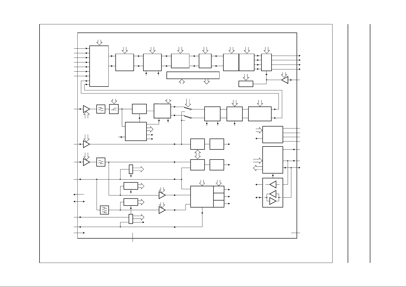
5 BLOCK DIAGRAM
Philips Semiconductors Product specification
Car radio integrated signal processor TEF6894H
CDL
CDR
CDCM
TAPEL
TAPER
PHONE
PHCM
FMMPX
AM
MPXRDS
LEVEL
SCLG
SDAG
AFSAMP
AFHOLD
FREF
input select
22
+
20
+
21
−
24
+
level
sclg
sdag
f
INPUT
+
SELECT
+
−
+
+
MPX
USN
WAM
ref
23
25
26
5
7
6
1
3
4
10
9
11
0 to −20 dB
low f: 50/100 Hz
high boost
LOUDNESS
asi
19 kHz
REFERENCE
f
ref
TEF6894H
DETECT
DETECT
vol: +20 to −59 dB
bal: L/R, 0 to −79 dB
mute
VOLUME/
BALANCE/
MUTE
asi
38 kHz
level
usn
wam
afus
afumute
afu-
mute
STEREO
DECODER
stereo
57 kHz
I
ref
amfm-
softmute
PILOT
CANCEL
PILOT/
PLL
reset/hold
8, 12, 13, 14, 15, 19, 31, 33
34, 35, 36, 37, 38, 39, 40
i.c.
+14 to −14 dB
f: 8 to 15 kHz
TREBLE
AUDIO STEP INTERPOLATION (asi)
asi time asi active
stereo adjustroll-off correction fm/am
fmsnc
nb sensitivity
usn
sensitivity
wam
sensitivity
+14 to −14 dB
f: 60 to 120 Hz
shelve/band-pass
NOISE
DETECT
NOISE
DETECT
detection timings
and control
MULTIPATH/
WEAK SIGNAL
DETECTION
AND LOGIC
hold
BASS
asi
BLANKER
amnb
NOISE
PULSE
TIMER
PULSE
TIMER
fmnb
SNC
HCC
SM
front/rear
0 to −59 dB
FRONT/
REAR
FADER
f: 1.5 to 15 kHz/wide
amfmhcc
snc start, slope
hcc start, slope
sm start, slope
LF, RF,
LR, RR
MUTE
asi asi
BEEP
HIGH
CUT
amnb
fmnb
fmsnc
amfm-
hcc
amfm-
softmute
mute:
level/off
pitch
50/75 µs
DE-EMPHASIS
standby
V
ref
sclg
sdag
mix:
LF, RF,
LR, RR
MIX
SUPPLY
2
I
C-BUS
INTERFACE
read
write
autogate
on/off
addr
27
28
29
30
32
16
17
18
41
44
43
42
MHC422
LFOUT
RFOUT
LROUT
RROUT
NAV
V
CC
AGND
CREF
DGND
ADDR
SCL
SDA
2
GND
handbook, full pagewidth
Fig.1 Block diagram.
Page 7

Philips Semiconductors Product specification
Car radio integrated signal processor TEF6894H
6 PINNING
SYMBOL PIN DESCRIPTION
LEVEL 1 level detector input
GND 2 ground
SCLG 3 gated I
SDAG 4 gated I
FMMPX 5 FM-MPX input for audio processing
MPXRDS 6 FM-MPX input for weak signal processing and noise blanker
AM 7 AM audio input
i.c. 8 internally connected
AFHOLD 9 FM weak signal processing hold input
AFSAMP 10 trigger signal input for quality measurement
FREF 11 reference frequency input 75.4 kHz
i.c. 12 internally connected
i.c. 13 internally connected
i.c. 14 internally connected
i.c. 15 internally connected
V
CC
16 supply voltage
AGND 17 analog ground
CREF 18 reference voltage capacitor
i.c. 19 internally connected
CDR 20 CD right input
CDCM 21 CD common input
CDL 22 CD left input
TAPER 23 tape right input
TAPEL 24 tape left input
PHONE 25 phone input
PHCM 26 phone common input
LFOUT 27 left front output
RFOUT 28 right front output
LROUT 29 left rear output
RROUT 30 right rear output
i.c. 31 internally connected
NAV 32 audio input for navigation voice signal
i.c. 33 internally connected
i.c. 34 internally connected
i.c. 35 internally connected
i.c. 36 internally connected
i.c. 37 internally connected
i.c. 38 internally connected
i.c. 39 internally connected
i.c. 40 internally connected
2
C-bus clock port
2
C-bus data port
2003 Oct 21 7
Page 8
Philips Semiconductors Product specification
Car radio integrated signal processor TEF6894H
SYMBOL PIN DESCRIPTION
DGND 41 digital ground
SDA 42 I
SCL 43 I
ADDR 44 address select input
handbook, full pagewidth
2
C-bus data input or output
2
C-bus clock input
ADDR
SCL
SDA
44
43
42
DGND
41
i.c.
40
i.c.
39
i.c.
38
i.c.
37
i.c.
36
i.c.
35
i.c.
34
1
LEVEL
2
GND
3
SCLG
4
SDAG
AM
i.c.
FREF
5
14
i.c.
TEF6894H
15
i.c.
6
7
8
9
10
11
12
13
i.c.
i.c.
FMMPX
MPXRDS
AFHOLD
AFSAMP
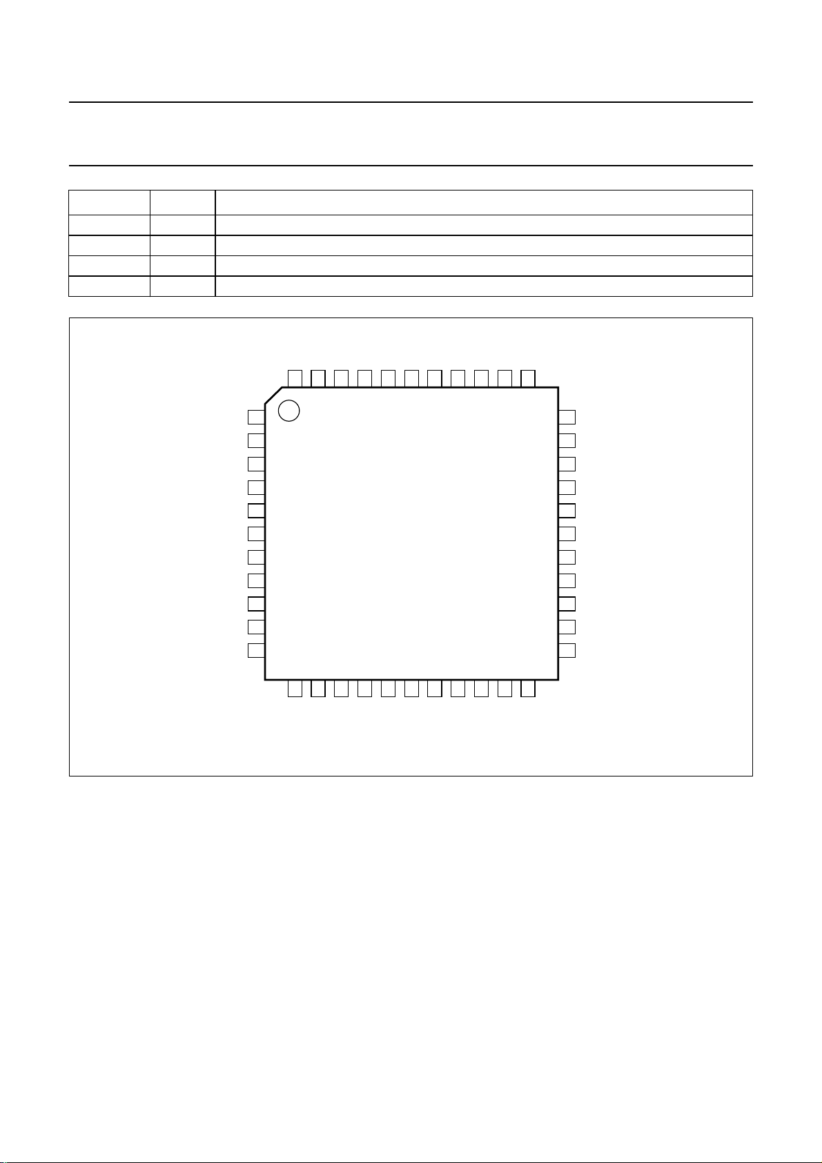
Fig.2 Pin configuration.
7 FUNCTIONAL DESCRIPTION
7.1 Stereo decoder
The FMMPX input is the input for the MPX signal from the
tuner. The input gain can be selected in three settings to
match the input to the RF front-end circuit. A fourth setting
is used for weather band mode, which may require a gain
of 23.5 dB.
A low-pass filter provides the necessary signal delay for
FM noise blanking and suppression of high frequency
interferences into the stereo decoder input. The output
signalofthisfilterisfedtotheroll-offcorrectioncircuit.This
circuit compensates the frequency response caused by
the low-pass characteristic of the tuner circuit with its
IF filters. The roll-off correction circuit is adjustable in four
33
i.c.
32
NAV
31
i.c.
30
RROUT
29
LROUT
28
RFOUT
27
LFOUT
26
PHCM
25
PHONE
24
TAPEL
23
TAPER
16
17
18
19
20
21
22
MHC421
CC
V
AGND
CREF
i.c.
CDR
CDCM
CDL
settings to compensate different frequency responses of
the tuner part.
The MPX signal is decoded in the stereo decoder part.
A PLL is used for the regeneration of the 38 kHz
subcarrier. The fully integrated oscillator is adjusted by a
digitalauxiliaryPLLintothecapturerangeofthemain PLL.
The auxiliary PLL needs an external reference frequency
(75.4 kHz) which is provided by the tuner ICs of the NICE
family(TEA684x). The required 19 and 38 kHz signals are
generated by division of the oscillator output signal in a
logic circuit. The 19 kHz quadrature phase signal is fed to
the 19 kHz phase detector, where it is compared with the
incoming pilot tone. The DC output signal of the phase
detector controls the oscillator (PLL).
2003 Oct 21 8
Page 9

Philips Semiconductors Product specification
Car radio integrated signal processor TEF6894H
The pilot detector is driven by an internally generated
in-phase 19 kHz signal. Its pilot dependent voltage
activates the stereo indicator bit and sets the stereo
decoder to stereo mode. The same voltage is used to
controlthe amplitude of an anti-phase internally generated
19 kHz signal. In the pilot canceller, the pilot tone is
compensated by this anti-phase 19 kHz signal.
The signal is then decoded in the decoder part. The side
signal is demodulated and combined with the main signal
to the left and right audio channels. A fine adjustment of
the roll-off compensation is done by adjusting the gain of
the L-R signal in 16 steps. A smooth mono to stereo
takeover is achieved by controlling the efficiency of the
matrix by the FMSNC signal from the weak signal
processing block.
7.2 FM and AM noise blanker
The FM/AM switch selects the output signal of the stereo
decoder (FM mode) or the signal from the AM input for the
noise blanker block. In FM mode the noise blanker
operates as a sample and hold circuit, while in AM mode it
mutes the audio signal during the interference pulse. The
blanking pulse which triggers the noise blanker is
generated in the noise detector block.
7.3 High cut control and de-emphasis
The High Cut Control (HCC) part is a low-pass filter circuit
with eight different static roll-off response curves. The
cut-offfrequenciesofthesefiltercurvescanbeselectedby
I2C-bus to match different application requirements. The
HCC circuit also provides a dynamic control of the filter
response. This function is controlled by the AMFMHCC
signal from the weak signal processing.
The signal passes the de-emphasis block with two
de-emphasisvalues(50and75 µs), which can be selected
via I2C-bus, and is fed to the input selector.
7.4 Noise detector
7.4.1 FM NOISE DETECTOR Thetrigger signal for the FMnoise detector is derived from
the MPXRDS input signal and the LEVEL signal. In the
MPXRDS path a four pole high-pass filter (100 kHz)
separates the noise spikes from the wanted MPX signal.
Another detector circuit triggers on noise spikes on the
level voltage. The signals of both detectors are combined
to achieve a reliable trigger signal for the noise blanker.
AGC circuits in the detector part control the gain
depending on the average noise in the signals to prevent
false triggering. The sensitivity of the triggering from the
MPXRDS signal can be adjusted in four steps, the
triggering from the LEVEL signal in three steps.
7.4.2 AM NOISE DETECTOR The trigger pulse for the AM noise blanker is derived from
the AM audio signal. The noise spikes are detected by a
slew rate detector, which detects excessive slew rates
which do not occur in normal audio signals. The sensitivity
of the AM noise blanker can be adjusted in four steps.
7.5 Multipath/weak signal processing
The multipath (MPH)/weak signal processing block
detectsqualitydegradationsintheincomingFMsignaland
controls the processing of the audio signal accordingly.
There are three different quality criteria:
• The average value of the level voltage
• The AM components on the level voltage
[Wideband AM (WAM)]
• The high frequency components in the MPX signal
[Ultrasonic Noise (USN)].
The level voltage is converted to a digital value by an 8-bit
analog-to-digital converter. A digital filter circuit (WAM
filter) derives the wideband AM components from the level
signal.ThehighfrequencycomponentsintheMPXsignals
are measured with an analog-to-digital converter (USN
ADC) at the output of the 100 kHz high-pass filter in the
MPXRDS path.
The values of these three signals are externally available
via the I2C-bus.
In the weak signal processing block the three digital
signals are combined in a specific way and used for the
generation of control signals for soft mute, stereo blend
(stereo noise control, FMSNC) and high cut control
(AMFMHCC).
The sensitivities of the detector circuits (WAM and USN)
are adjustable via the I2C-bus.
Alsothestartvaluesandtheslopesofthecontrolfunctions
soft mute, stereo blend and high cut control can be set via
the I2C-bus.
Soft mute, stereo blend and HCC are set on hold during
the AF updating (quality check of alternative frequency) to
avoid an influence of the tuning procedure on the weak
signal processing conditions.
In AM mode the soft mute and high cut control are
available too, the weak signal block is controlled by the
average value of the level voltage.
2003 Oct 21 9
Page 10

Philips Semiconductors Product specification
Car radio integrated signal processor TEF6894H
7.6 Tone/volume control
The tone/volume control part consists of the following
stages:
• Input selector
• Loudness control
• Volume/balance control with muting
• Treble control
• Bass control
• Fader and output mute
• Beep generator
• NAV input
• Output mixer.
The settings of all stages are controlled via the I2C-bus.
The stages input selector, loudness, volume/balance,
bass, and fader/output mute include the Audio Step
Interpolation (ASI) function. This minimizes pops by
smoothing the transitions in the audio signal during the
switching of the controls. The transition time of the ASI
function is programmable by I2C-bus in four steps.
7.6.1 INPUT SELECTOR
7.6.4 TREBLE
The signal is then fed to the treble control stage. The
control range is between +14 and −14 dB in steps of 2 dB.
Figure 20 shows the control characteristic. Four different
filter frequencies can be selected.
7.6.5 BASS
The characteristic of the bass attenuation curves can be
set to shelve or band-pass. Four different frequencies can
be selected as centre frequency of the band-pass curve.
Figures 21 and 22show the bass curves with a band-pass
filter frequency of 60 Hz. The control range is between
+14 and −14 dB in steps of 2 dB.
7.6.6 FADER/MUTE
The four fader/mute blocks are located at the end of the
tone/volume chain. The control range of these attenuators
is 0 to −59 dB. The step size is:
• 1 dB between 0 and −15 dB
• 2.5 dB between −15 and −45 dB
• 3 dB between −45 and −51 dB
• 4 dB between −51 and −59 dB.
The input selector selects one of four input sources:
• Two external stereo inputs (CD and TAPE)
• One external mono input (PHONE)
• One internal stereo input (AM/FM).
7.6.2 LOUDNESS The output of the input selector is fed into the loudness
circuit. Four different loudness curves can be selected via
the I2C-bus. The control range is between 0 and −20 dB
with a step size of 1 dB; see Figs 16 to 19.
7.6.3 VOLUME/BALANCE Thevolume/balance control is used for volumesetting and
also for balance adjustment. The control range of the
volume/balance control is between +20 and −59 dB in
steps of 1 dB.
Thecombination of loudness and volume/balance realizes
an overall control range of +20 to −79 dB.
7.6.7 BEEP GENERATOR AND NAVINPUT WITH OUTPUT
MIXER
The output mixer circuit can add anadditional audio signal
to any of the four outputs together with the main signal or
instead of the main signal.
The additional signal can be generated internally by the
beep generator with four different audio frequencies or
applied to the NAV input, for instance a navigation voice
signal.
2003 Oct 21 10
Page 11

Philips Semiconductors Product specification
Car radio integrated signal processor TEF6894H
8 LIMITING VALUES
In accordance with the Absolute Maximum Rating System (IEC 60134).
SYMBOL PARAMETER CONDITIONS MIN. MAX. UNIT
V
CC
V
i
T
stg
T
amb
V
esd
Notes
1. Machine model (R = 0 Ω, C = 200 pF).
2. Human body model (R = 1.5 kΩ, C = 100 pF).
9 THERMAL CHARACTERISTICS
supply voltage −0.3 +10 V
input voltage for any pin −0.3 VCC+ 0.3 V
storage temperature −65 +150 °C
ambient temperature −40 +85 °C
electrostatic discharge voltage note 1 −200 +200 V
note 2 −2000 +2000 V
SYMBOL PARAMETER CONDITIONS VALUE UNIT
R
th(j-a)
thermal resistance from junction to ambient in free air 61 K/W
10 CHARACTERISTICS
FM part: f
V
= 967 mV (RMS) (100% AM). Treble: 10 kHz filter frequency. Bass: 60 Hz filter frequency. Loudness: 50 Hz filter
AM
frequency; treble loudness on. V
FMMPX
= 1 kHz at V
= 767 mV (RMS); pilot off (100% FM). AM part: fAM= 1 kHz at
FMMPX
= 8.5 V; T
CC
=25°C; see Fig.23; unless otherwise specified.
amb
SYMBOL PARAMETER CONDITIONS MIN. TYP. MAX. UNIT
V
CC
I
CC
supply voltage 8.0 8.5 9.0 V
supply current normal mode − 24 − mA
standby − 15 − mA
Logic pins
V
IH
HIGH-level input voltage pins SDA, SCL, ADDR and SDAG 1.75 − 5.5 V
pins AFHOLD and AFSAMP 1.75 − 5.5 V
V
IL
LOW-level input voltage pins SDA, SCL, ADDR and SDAG −0.2 − +1.0 V
pins AFHOLD and AFSAMP −0.2 − +1.0 V
V
OL
LOW-level output voltage pin SCLG; IOL= 3 mA; note 1 −− 0.4 V
pin SDA; I
=3mA −− 0.4 V
OL
Stereo decoder and AM path
V
o(FM)(rms)
FM mono output voltage
(RMS value) on
f
= 1 kHz; 91% FM modulation
FMMPX
without pilot (V
FMMPX
750 950 1200 mV
= 698 mV)
pins LFOUT and RFOUT
V
o(AM)(rms)
AM output voltage
(RMS value) on
fAM= 1 kHz; VAM= 870 mV;
90% AM modulation
800 1080 1360 mV
pins LFOUT and RFOUT
2003 Oct 21 11
Page 12

Philips Semiconductors Product specification
Car radio integrated signal processor TEF6894H
SYMBOL PARAMETER CONDITIONS MIN. TYP. MAX. UNIT
G
i
α
cs
g
c(L-R)
g
f(L-R)
S/N signal-to-noise ratio f
THD total harmonic distortion FM mode
V
o(bal)
α
19
α subcarrier suppression modulation off; referenced to 1 kHz
PSRR power supply ripple
input gain on
pins FMMPX, MPXRDS
and AM
see Table 36
ING[1:0] = 00; all inputs − 0 − dB
ING[1:0] = 01; all inputs − 3 − dB
ING[1:0] = 10; all inputs − 6 − dB
ING[1:0] = 11; FMMPX − 23.5 − dB
ING[1:0] = 11; MPXRDS and AM − 0 − dB
channel separation f
roll-off correction for
coarse adjustment of
separation
see Table 20; measure 1 kHz level
for L − R modulation; compare to
1 kHz level for L + R modulation
= 1 kHz 40 −−dB
FMMPX
CSR[1:0] = 00 − 0 − dB
CSR[1:0] = 01 − 0.4 − dB
CSR[1:0] = 10 − 0.8 − dB
CSR[1:0] = 11 − 1.2 − dB
stereo adjust for fine
adjustment of separation
see Table 21; measure 1 kHz level
for L − R modulation; compare to
1 kHz level for L + R modulation
CSA[3:0] = 0000 − 0 − dB
CSA[3:0] = 0001 − 0.2 − dB
: − : − dB
CSA[3:0] = 1110 − 2.8 − dB
CSA[3:0] = 1111 − 3.0 − dB
= 20 Hz to 15 kHz;
FMMPX
75 −−dB
referenced to 1 kHz at 91% FM
modulation; DEMP = 1
(τ
=50µs)
de-em
f
V
V
= 1 kHz −− 0.3 %
FMMPX
= 50%; L; pilot on −− 0.3 %
FMMPX
= 50%; R; pilot on −− 0.3 %
FMMPX
mono channel balance FM mode −1 − +1 dB
V
oL
--------- V
oR
pilot signal suppression 9% pilot; f
= 19 kHz; referenced
pilot
40 50 − dB
to 1 kHz at 91% FM modulation;
DEMP = 1 (τ
de-em
=50µs)
at 91% FM modulation
= 38 kHz 35 50 − dB
f
sc
f
= 57 kHz 40 −−dB
sc
= 76 kHz 50 60 − dB
f
sc
rejection
FM mode; f
V
CC(AC)=Vripple
= 100 Hz;
ripple
= 100 mV (RMS)
24 −−dB
2003 Oct 21 12
Page 13

Philips Semiconductors Product specification
Car radio integrated signal processor TEF6894H
SYMBOL PARAMETER CONDITIONS MIN. TYP. MAX. UNIT
∆V
out
f
cut-off(de-em)
m
i(pilot)(rms)
hys
pilot
V
ref(min)
f
ref
Noise blanker
frequency response FM mode
f
FMMPX
f
FMMPX
cut-off frequency of
de-emphasis filter
−3 dB point; see Fig.15
DEMP = 1 (τ
DEMP = 0 (τ
pilot threshold modulation
forautomatic switching by
pilot input voltage
(RMS value)
stereo
on − 4.0 5.5 %
off 1.3 2.7 − %
hysteresis of pilot
threshold voltage
minimum reference input
voltage
reference frequency for
stereo PLL
=20Hz −0.5 − +0.5 dB
= 15 kHz −0.5 − +0.5 dB
=50µs) − 3.18 − kHz
de-em
=75µs) − 2.12 − kHz
de-em
− 2 − dB
−− 30 mV
75361 75368 75375 Hz
FM PART
t
sup(min)
V
MPXRDS(M)
V
LEVEL(M)
AM
PART
t
sup(min)
M
AM
minimum suppression
time
noise blanker sensitivity
at MPXRDS input
(peak value of noise
pulses)
see Table 37; t
repetition frequency f = 300 Hz
NBS[1:0] = 00 − 90 − mV
NBS[1:0] = 01 − 150 − mV
NBS[1:0] = 10 − 210 − mV
NBS[1:0] = 11 − 270 − mV
noise blanker sensitivity
at LEVEL input
(peak value of noise
pulses)
see Table 40; t
repetition frequency f = 300 Hz
NBL[1:0] = 00 − 9 − mV
NBL[1:0] = 01 − 18 − mV
NBL[1:0] = 10 − 28 − mV
minimum suppression
time
noise blanker sensitivity see Table 37; f
NBS[1:0] = 00 − 110 − %
NBS[1:0] = 01 − 140 − %
NBS[1:0] = 10 − 175 − %
NBS[1:0] = 11 − 220 − %
pulse
pulse
audio
− 15 −µs
=10µs;
=10µs;
− 200 −µs
= 2 kHz
2003 Oct 21 13
Page 14

Philips Semiconductors Product specification
Car radio integrated signal processor TEF6894H
SYMBOL PARAMETER CONDITIONS MIN. TYP. MAX. UNIT
Weak signal processing
DETECTORS
V
eq(USN)
V
eq(WAM)
t
LEVEL(attack)
t
LEVEL(decay)
USNsensitivityequivalent
level voltage
WAM sensitivity
equivalent level voltage
level detector attack time
(soft mute and HCC)
level detector decay time
(soft mute and HCC)
see Fig.5; f
V
MPXRDS
MPXRDS
= 250 mV (RMS);
= 150 kHz;
HCMP = 1; note 2
USS[1:0] = 00 − 2.5 − V
USS[1:0] = 01 − 2 − V
USS[1:0] = 10 − 1.5 − V
USS[1:0] = 11 − 0.5 − V
see Fig.6; V
= 200 mV (p-p) at
LEVEL
f = 21 kHz on the level voltage;
HCMP = 1; note 2
WAS[1:0] = 00 − 2.5 − V
WAS[1:0] = 01 − 2 − V
WAS[1:0] = 10 − 1.5 − V
WAS[1:0] = 11 − 0.5 − V
see Table 24; LETF = 0; SEAR = 0
LET[1:0] = 00 − 3 − s
LET[1:0] = 01 − 3 − s
LET[1:0] = 10 − 1.5 − s
LET[1:0] = 11 − 0.5 − s
see Table 24; LETF = 1; SEAR = 0
LET[1:0] = 00 − 0.5 − s
LET[1:0] = 01 − 0.17 − s
LET[1:0] = 10 − 0.06 − s
LET[1:0] = 11 − 0.06 − s
search mode; SEAR = 1 − 60 − ms
see Table 24; LETF = 0; SEAR = 0
LET[1:0] = 00 − 3 − s
LET[1:0] = 01 − 6 − s
LET[1:0] = 10 − 1.5 − s
LET[1:0] = 11 − 1.5 − s
see Table 24; LETF = 1; SEAR = 0
LET[1:0] = 00 − 0.5 − s
LET[1:0] = 01 − 0.5 − s
LET[1:0] = 10 − 0.17 − s
LET[1:0] = 11 − 0.06 − s
search mode; SEAR = 1 − 60 − ms
2003 Oct 21 14
Page 15

Philips Semiconductors Product specification
Car radio integrated signal processor TEF6894H
SYMBOL PARAMETER CONDITIONS MIN. TYP. MAX. UNIT
t
MPH(attack)
t
MPH(decay)
t
USN(attack)
t
USN(decay)
∆USS USN detector
t
WAM(attack)
t
WAM(decay)
t
peak(USN)(attack)
t
peak(USN)(decay)
t
peak(WAM)(attack)
t
peak(WAM)(decay)
multipath detector attack
time (SNC)
multipath detector decay
time (SNC)
USN detector attack time
(soft mute and SNC)
USN detector decay time
(soft mute and SNC)
desensitization
WAMdetector attack time
(SNC)
WAMdetector decay time
(SNC)
peak detector for USN
attack time for read-out
via I2C-bus
peak detector for USN
decay time for read-out
via I2C-bus
peak detector for WAM
attack time for read-out
via I2C-bus
peak detector for WAM
decay time for read-out
via I2C-bus
see Table 25; SEAR = 0
MPT[1:0] = 00 − 0.5 − s
MPT[1:0] = 01 − 0.5 − s
MPT[1:0] = 10 − 0.5 − s
MPT[1:0] = 11 − 0.25 − s
search mode; SEAR = 1 − 60 − ms
see Table 25; SEAR = 0
MPT[1:0] = 00 − 12 − s
MPT[1:0] = 01 − 24 − s
MPT[1:0] = 10 − 6 − s
MPT[1:0] = 11 − 6 − s
search mode; SEAR = 1 − 60 − ms
− 1 − ms
− 1 − ms
USN sensitivity setting (USS) versus
levelvoltage (USN sensitivity setting
is automatically reduced as level
voltage decreases)
V
1.25V>V
1.125 V > V
1.0V>V
> 1.25 V −− 3−
LEVEL
> 1.125 V −− 2−
LEVEL
> 1.0 V −− 1−
LEVEL
LEVEL
−− 0−
− 1 − ms
− 1 − ms
− 1 − ms
− 10 − ms
− 1 − ms
− 10 − ms
2003 Oct 21 15
Page 16

Philips Semiconductors Product specification
Car radio integrated signal processor TEF6894H
SYMBOL PARAMETER CONDITIONS MIN. TYP. MAX. UNIT
CONTROL FUNCTIONS
V
start(mute)
C
mute
α
mute(max)
V
start(SNC)
C
SNC
soft mute start voltage see Fig.12; voltage at pin LEVEL
that causes α
mute
= 3 dB;
MSL[1:0] = 11
MST[2:0] = 000 − 0.75 − V
MST[2:0] = 001 − 0.88 − V
MST[2:0] = 010 − 1 − V
MST[2:0] = 011 − 1.12 − V
MST[2:0] = 100 − 1.25 − V
MST[2:0] = 101 − 1.5 − V
MST[2:0] = 110 − 1.75 − V
MST[2:0] = 111 − 2 − V
soft mute slope see Fig.13; slope of soft mute
C
mute
=
α
∆
mute
-----------------
∆
V
eq
attenuation with respect to level
voltage; MST[2:0] = 000
MSL[1:0] = 00 − 8 − dB/V
MSL[1:0] = 01 − 16 − dB/V
MSL[1:0] = 10 − 24 − dB/V
MSL[1:0] = 11 − 32 − dB/V
maximum soft mute
attenuation by USN
see Fig.14; f
V
MPXRDS
= 0.6 V (RMS);
MPXRDS
= 150 kHz;
USS[1:0] = 11
UMD[1:0] = 00 − 3 − dB
UMD[1:0] = 01 − 6 − dB
UMD[1:0] = 10 − 9 − dB
UMD[1:0] = 11 − 12 − dB
SNC stereo blend start
voltage
see Fig.7; voltage at pin LEVEL that
causes channel separation = 10 dB;
SSL[1:0] = 10
SST[3:0] = 0000 − 1.5 − V
: − : − V
SST[3:0] = 1000 − 2.0 − V
: − : − V
SST[3:0] = 1111 − 2.45 − V
SNC slope see Fig.8; slope of channel
C
SNC
=
αcs∆
------------ -
∆
V
eq
separation between
30 dB and 10 dB with respect to
level voltage; SST[3:0] = 1010
SSL[1:0] = 00 − 38 − dB/V
SSL[1:0] = 01 − 51 − dB/V
SSL[1:0] = 10 − 63 − dB/V
SSL[1:0] = 11 − 72 − dB/V
2003 Oct 21 16
Page 17

Philips Semiconductors Product specification
Car radio integrated signal processor TEF6894H
SYMBOL PARAMETER CONDITIONS MIN. TYP. MAX. UNIT
V
start(HCC)
C
HCC
α
HCC(max)
f
cut-off
Analog-to-digital converters for I
HCC start voltage see Fig.9; f
pin LEVEL that causes α
HSL[1:0] = 10
HST[2:0] = 000 − 1.17 − V
HST[2:0] = 001 − 1.42 − V
HST[2:0] = 010 − 1.67 − V
HST[2:0] = 011 − 1.92 − V
HST[2:0] = 100 − 2.17 − V
HST[2:0] = 101 − 2.67 − V
HST[2:0] = 110 − 3.17 − V
HST[2:0] = 111 − 3.67 − V
HCC slope see Fig.10; f
C
HCC
=
α
∆
HCC
-----------------
∆
V
eq
HST[2:0] = 010
HSL[1:0] = 00 − 9 − dB/V
HSL[1:0] = 01 − 11 − dB/V
HSL[1:0] = 10 − 14 − dB/V
HSL[1:0] = 11 − 18 − dB/V
maximum HCC
attenuation
see Fig.10; f
HCSF = 1 − 10 − dB
HCSF = 0 − 14 − dB
cut-off frequency of fixed
HCC
see Table 31; −3 dB point (first order
filter)
HCF[2:0] = 000 − 1.5 − kHz
HCF[2:0] = 001 − 2.2 − kHz
HCF[2:0] = 010 − 3.3 − kHz
HCF[2:0] = 011 − 4.7 − kHz
HCF[2:0] = 100 − 6.8 − kHz
HCF[2:0] = 101 − 10 − kHz
HCF[2:0] = 110 − wide −−
HCF[2:0] = 111 − unlimited −−
2
C-bus
= 10 kHz; voltage at
audio
= 10 kHz;
audio
=10kHz
audio
HCC
= 3 dB;
LEVEL ANALOG-TO-DIGITAL CONVERTER (8-BIT); see Fig.4
V
LEVEL(min)
lower voltage limit of
conversion range
V
LEVEL(max)
upper voltage limit of
conversion range
∆V
LEVEL
bit resolution voltage − 15.7 − mV
2003 Oct 21 17
− 0.25 − V
− 4.25 − V
Page 18

Philips Semiconductors Product specification
Car radio integrated signal processor TEF6894H
SYMBOL PARAMETER CONDITIONS MIN. TYP. MAX. UNIT
ULTRASONIC NOISE ANALOG-TO-DIGITAL CONVERTER (4-BIT); see Fig.5
V
USN(min)(rms)
conversion range lower
voltage limit (RMS value)
V
USN(max)(rms)
conversion range upper
voltage limit (RMS value)
∆V
USN(rms)
bit resolution voltage
(RMS value)
WIDEBAND AM ANALOG-TO-DIGITAL CONVERTER (4-BIT); see Fig.6
V
WAM(min)(p-p)
lower voltage limit of
conversion range
(peak-to-peak value)
V
WAM(max)(p-p)
upper voltage limit of
conversion range
(peak-to-peak value)
∆V
WAM(p-p)
bit resolution voltage
(peak-to-peak value)
Tone/volume control
Z
i
input impedance at pins
TAPEL, TAPER, CDL and
CDR
input impedance at
pin PHONE
Z
o
output impedance at
pins LFOUT, RFOUT,
LROUT and RROUT
G
s(main)
signal gain from main
source input to LFOUT,
RFOUT, LROUT and
RROUT outputs
G
s(NAV)
signal gain from NAV
input to LFOUT, RFOUT,
LROUT and RROUT
outputs
V
i(max)(rms)
maximum input voltage
level at pins TAPEL,
TAPER, CDL, CDR and
PHONE (RMS value)
V
i(NAV)(max)(rms)
maximum input voltage
level at pin NAV
(RMS value)
V
o(max)(rms)
maximum output voltage
(RMS value)
f
f
= 150 kHz − 0 − V
FMMPX
= 150 kHz − 0.75 − V
FMMPX
− 50 − mV
f
=21kHz − 0 − mV
LEVEL
f
=21kHz − 800 − mV
LEVEL
− 53.3 − mV
80 −−kΩ
50 −−kΩ
−− 100 Ω
−1 − +1 dB
−1.5 0 +1.5 dB
THD = 0.1%; G
= −6dB 2 −−V
vol
THD = 1% 0.3 −−V
THD = 0.1%; G
worst case load: R
=+6dB 2 −−V
vol
=2kΩ,
L
2 −−V
CL= 10 nF, THD = 1%
2003 Oct 21 18
Page 19

Philips Semiconductors Product specification
Car radio integrated signal processor TEF6894H
SYMBOL PARAMETER CONDITIONS MIN. TYP. MAX. UNIT
f
max
CMRR common mode rejection
α
cs
α
S
THD total harmonic distortion TAPE and CD inputs
V
noise(rms)
∆G
step
frequency response
(pins TAPER, TAPEL,
CDR and CDL)
ratio
channel separation f
input isolation of one
selected source to any
other input
noise voltage
(RMS value)
step error (all controls)
between all adjoining
steps, all outputs
upper −0.5 dB point; referenced
20 −−kHz
to 1 kHz
f
= 20 Hz to 20 kHz on CD and
audio
PHONE inputs
G
=0dB 40 −−dB
vol
= −15 dB 55 −−dB
G
vol
= 20 Hz to 20 kHz 60 80 − dB
audio
f
= 1 kHz 90 105 − dB
audio
= 20 Hz to 10 kHz 75 90 − dB
f
audio
f
= 20 kHz 70 −−dB
audio
f
= 20 Hz to 10 kHz;
audio
− 0.01 0.1 %
Vi= 1 V (RMS)
= 1 kHz; Vi= 2 V (RMS);
f
audio
G
=0dB
vol
f
= 20 Hz to 10 kHz;
audio
Vi= 2 V (RMS); G
= 25 Hz;Vi= 500 mV (RMS);
f
audio
G
= +8 dB; G
bass
f
= 4 kHz;Vi= 500 mV (RMS);
audio
G
= +8 dB; G
treble
NAV input; f
audio
= −10 dB
vol
=0dB
vol
=0dB
vol
= 1 kHz;
− 0.02 0.1 %
− 0.02 0.2 %
− 0.05 0.2 %
− 0.01 0.2 %
−− 1%
Vo= 300 mV (RMS)
CCIR-ARM weighted and 20 kHz
‘brick wall’ without input signal and
shorted AF inputs
G
=0dB − 12 20 µV
vol
= +6 dB; G
G
bass
G
=0dB
vol
G
= 20 dB; TAPE input (stereo) − 71 100 µV
vol
G
= 20 dB; CD input
vol
treble
=+6dB;
− 24 35 µV
− 100 140 µV
(quasi-differential)
G
= −10 dB − 10 18 µV
vol
G
= −40 dB; G
vol
loudness
= −20 dB − 9.5 13.5 µV
outputs muted − 512µV
using ‘A-weighting’ filter and
20 kHz ‘brick wall’; G
G
loudness
= −10 dB
= −10 dB;
vol
− 6.8 10 µV
NAV input − 16 40 µV
G = +20 to −36 dB −− 0.5 dB
G=−36 to −59 dB −− 1.0 dB
2003 Oct 21 19
Page 20

Philips Semiconductors Product specification
Car radio integrated signal processor TEF6894H
SYMBOL PARAMETER CONDITIONS MIN. TYP. MAX. UNIT
TC
ASI
V
offset(max)
PSRR power supply ripple
α
ct
t
turn-on
LOUDNESS
f
loudness(low)
f
loudness(high)
G
loudness
V
OLUME
G
vol
G
step(vol)
ASI time constant
(switching time from any
setting to any other
setting)
see Table 42
AST[1:0] = 00 − 1 − ms
AST[1:0] = 01 − 3 − ms
AST[1:0] = 10 − 10 − ms
AST[1:0] = 11 − 30 − ms
maximum DC offset between any two settings
(non-consecutive) on any one audio
control or any one dynamic weak
signal processing control
= 200 mV (RMS)
rejection
crosstalk between bus
V
CC(AC)=Vripple
f
= 20 to 100 Hz 35 46 − dB
ripple
f
= 1 kHz 50 75 − dB
ripple
f
= 1 to 20 kHz 50 65 − dB
ripple
f
= 100 kHz; note 3 − 110 − dB
clk
inputs and signal outputs
turn-on time from V
CC
applied to 66% final DC
voltage at outputs
loudness low boost
frequency without
influence of coupling
capacitors
loudness filter response
without influence of
coupling capacitors
loudness gain control f
amplitude decrease = −3dB
LLF = 0 − 50 − Hz
LLF = 1 − 100 − Hz
amplitude decrease = −1 dB;
frequency referred to 100 kHz;
high boost on
loudness(low)
= 50 Hz; high boost on;
see Fig.16
maximum setting; 1 kHz tone − 0 − dB
minimum setting; 1 kHz tone −−20 − dB
minimum setting; 50 Hz tone −−3 −dB
minimum setting; 10 kHz tone −−16 − dB
minimum setting; 100 kHz tone −−15 − dB
step size; 1 kHz tone − 1 − dB
volume/balance gain
control
see Table 48
maximum setting − 20 − dB
minimum setting −−59 − dB
mute attenuation; 20 Hz to 20 kHz
input
step resolution gain
see Table 48 − 1 − dB
(volume)
− 7 − mV
− 100 − ms
− 10 − kHz
−−80 −70 dB
2003 Oct 21 20
Page 21

Philips Semiconductors Product specification
Car radio integrated signal processor TEF6894H
SYMBOL PARAMETER CONDITIONS MIN. TYP. MAX. UNIT
∆G
set
∆G
track
TREBLE
f
cut-off(treble)
G
treble
G
step(treble)
BASS
f
c(bass)
Q
bass
EQ
bow
G
bass
G
step(bass)
FADER
G
fader
gain set error G
gain tracking error
between left and right
treble control filter cut-off
frequency
= +20 to −36 dB −1 0 +1 dB
vol
G
= −36 to −59 dB −3 0 +3 dB
vol
G
= +20 to −36 dB − 01dB
vol
G
= −36 to −59 dB − 03dB
vol
see Table 52; −3 dB frequency
referenced to 100 kHz
TRF[1:0] = 00 − 8 − kHz
TRF[1:0] = 01 − 10 − kHz
TRF[1:0] = 10 − 12 − kHz
TRF[1:0] = 11 − 15 − kHz
treble gain control see Table 51
maximum setting − 14 − dB
minimum setting −−14 − dB
step resolution gain
see Table 51 − 2 − dB
(treble)
bass control filter centre
frequency
see Table 56
BAF[1:0] = 00 − 60 − Hz
BAF[1:0] = 01 − 80 − Hz
BAF[1:0] = 10 − 100 − Hz
BAF[1:0] = 11 − 120 − Hz
bass filter quality factor G
equalizer bowing f
= +12 dB − 1.0 −−
bass
= 1 kHz; Vi= 500 mV (RMS);
audio
G
= +12 dB; f
bass
G
= +12 dB;
treble
f
cut-off(treble)
bass gain control see Table 55
maximum setting; symmetrical
boost
minimum setting; asymmetrical cut −−14 − dB
minimum setting; symmetrical cut −−14 − dB
step resolution gain
see Table 55 − 2 − dB
(bass)
fader gain control see Table 59
maximum setting − 0 − dB
minimum setting −−59 − dB
mute attenuation; 20 Hz to 20 kHz
input
= 60 Hz;
c(bass)
= 10 kHz; see Fig.3
− 1.8 − dB
− 14 − dB
−−80 −66 dB
2003 Oct 21 21
Page 22

Philips Semiconductors Product specification
Car radio integrated signal processor TEF6894H
SYMBOL PARAMETER CONDITIONS MIN. TYP. MAX. UNIT
G
step(fader)
α
mute
BEEP
f
beep
V
beep(rms)
THD
beep
Power-on reset (all registers in default setting, outputs muted, standby mode)
V
th(POR)
step resolution gain
(fader)
see Table 59
G
=0to−15 dB − 1 − dB
fader
G
= −15 to −45 dB − 2.5 − dB
fader
G
= −45 to −51 dB − 3 − dB
fader
G
= −51 to −59 dB − 4 − dB
fader
audio mute volume control: mute and output
muted (bits MULF, MURF, MULR
and MURR)
beep generator frequency see Table 68
BEF[1:0] = 00 − 500 − Hz
BEF[1:0] = 01 − 1 − kHz
BEF[1:0] = 10 − 2 − kHz
BEF[1:0] = 11 − 3 − kHz
beep generator audio
level (RMS value)
see Table 67
BEL[2:0] = 000 − 0 − mV
BEL[2:0] = 001 − 13.3 − mV
BEL[2:0] = 010 − 18 − mV
BEL[2:0] = 011 − 28 − mV
BEL[2:0] = 100 − 44 − mV
BEL[2:0] = 101 − 60 − mV
BEL[2:0] = 110 − 90 − mV
BEL[2:0] = 111 − 150 − mV
total harmonic distortion
f
= 1 kHz or 2 kHz −− 7%
beep
of beep generator
threshold voltage of
Power-on reset
90 −−dB
− 6.3 − V
Notes
1. The LOW voltage of pin SCLG is influenced by V
SCL
: V
SCLG(LOW)
≥ V
SCL(LOW)
+ 0.22 V.
2. The equivalent level voltage is that value of the level voltage (at pin LEVEL) which results in the same weak signal
control effect (for instance HCC roll-off) as the output value of the specified detector (USN, WAM and MPH).
V
3. Crosstalk between bus inputs and signal outputs:
αct20log
=
bus(p-p)
-------------------- V
o(rms)
2003 Oct 21 22
Page 23

Philips Semiconductors Product specification
Car radio integrated signal processor TEF6894H
18
handbook, full pagewidth
V
o
(dB)
14
10
6
2
−2
−6
−10
−14
−18
10
G
= +12 and −12 dB.
bass
= +12 and −12 dB.
G
treble
f
cut-off(treble)
f
c(bass)
= 10 kHz.
= 60 Hz.
MHC330
+1.85
−1.90
2
10
3
10
4
10
f
audio
(Hz)
5
10
Fig.3 Equalizer bowing.
2003 Oct 21 23
Page 24

Philips Semiconductors Product specification
Car radio integrated signal processor TEF6894H
11 I2C-BUS PROTOCOL Table 1 Write mode
(1)
S
address (write) A
Notes
1. S = START condition.
2. A = acknowledge.
3. P = STOP condition.
Table 2 Read mode
(1)
S
address (read) A
Notes
1. S = START condition.
2. A = acknowledge.
3. NA = not acknowledge.
4. P = STOP condition.
(2)
(2)
subaddress A
data byte(s) A
(2)
(2)
data byte(s) A
data byte NA
(2)
(3)
(3)
P
(4)
P
Table 3 IC address byte
IC ADDRESS MODE
001100ADDR R/
Table 4 Description of IC address byte
BIT SYMBOL DESCRIPTION
7to2 − 001100+(ADDR) = IC address.
1 ADDR Address bit. 0 = pin ADDR is grounded; 1 = pin ADDR is floating.
0R/
WRead/Write. 0 = write mode; 1 = read mode.
11.1 Read mode
11.1.1 DATA BYTE 1; STATUS
Table 5 Format of data byte 1
BIT 7 BIT 6 BIT 5 BIT 4 BIT 3 BIT 2 BIT 1 BIT 0
STIN ASIA AFUS POR − ID2 ID1 ID0
W
2003 Oct 21 24
Page 25

Philips Semiconductors Product specification
Car radio integrated signal processor TEF6894H
Table 6 Description of data byte 1
BIT SYMBOL DESCRIPTION
7 STIN Stereo indicator. 0 = no pilot signal detected; 1 = pilot signal detected.
6 ASIA ASI active. 0 = not active; 1 = ASI step is in progress.
5 AFUS AF update sample. 0 = LEV, USN and WAM information is taken from main frequency
(continuous mode); 1 = LEV, USN and WAM information is taken from alternative
frequency. Continuous mode during AF update and sampled mode after AF update.
Sampled mode reverts to continuous main frequency information after read.
4 POR Power-on reset. 0 = standard operation (valid I2C-bus register settings); 1 = Power-on
reset detected since last read cycle (I2C-bus register reset). After read the bit will reset
to POR = 0.
3 − Reserved.
2 to 0 ID[2:0] Identification. TEF6894H device type identification; ID[2:0] = 100.
11.1.2 DATA BYTE 2; LEVEL
Table 7 Format of data byte 2
BIT 7 BIT 6 BIT 5 BIT 4 BIT 3 BIT 2 BIT 1 BIT 0
LEV7 LEV6 LEV5 LEV4 LEV3 LEV2 LEV1 LEV0
Table 8 Description of data byte 2
BIT SYMBOL DESCRIPTION
7 to 0 LEV[7:0] Level. 8-bit value of level voltage from tuner; see Fig.4.
handbook, halfpage
5
V
eq
(V)
4
3
2
1
0
05
1234
MHC331
]
LEV[7:0
255
0
V
(V)
LEVEL
Fig.4 Equivalent level voltage Veq(MPH and LEV detector) as a function of level voltage V
2003 Oct 21 25
LEVEL
.
Page 26

Philips Semiconductors Product specification
Car radio integrated signal processor TEF6894H
11.1.3 DATA BYTE 3; USN AND WAM
Table 9 Format of data byte 3
BIT 7 BIT 6 BIT 5 BIT 4 BIT 3 BIT 2 BIT 1 BIT 0
USN3 USN2 USN1 USN0 WAM3 WAM2 WAM1 WAM0
Table 10 Description of data byte 3
BIT SYMBOL DESCRIPTION
7 to 4 USN[3:0] Ultrasonic noise detector. USN content of the MPXRDS audio signal; see Fig.5.
3 to 0 WAM[3:0] Wideband AM detector. WAM content of the LEVEL voltage; see Fig.6.
11.2 Write mode Table 11 Format for subaddress byte with default setting
BIT 7 BIT 6 BIT 5 BIT 4 BIT 3 BIT 2 BIT 1 BIT 0
AIOF GATE SGAT SA4 SA3 SA2 SA1 SA0
− 00−−−−−
Table 12 Description of subaddress byte
BIT SYMBOL DESCRIPTION
7 AIOF Auto-increment off. 0 = auto-increment enabled; 1 = auto-increment disabled.
6GATEGate. 0=I
2
C-bus outputs (SDAG and SCLG) are controllable by the shortgate or the
autogate function; 1 = I2C-bus outputs are enabled.
2
5 SGAT Shortgate. 1=I
C-bus outputs (SDAG and SCLG) are enabled for a single
transmission following this control and disabled automatically.
4 to 0 SA[4:0] Data byte select. The subaddress value is auto-incremented when AIOF = 0 and will
revert from SA = 30 to SA = 0. SA = 31 can only be accessed via direct subaddress
selection, in which case auto-increment will revert from SA = 31 to SA = 0; see
Table 13.
Table 13 Selection of data byte
SA4 SA3 SA2 SA1 SA0 HEX
(1)
MNEMONIC ADDRESSED DATA BYTE
000102RDSCLK test control
001004CONTROL control of supply and AF update
001015CSALIGN alignment of stereo channel separation
001106MULTIPATHcontrol of weak signal sensitivity and
timing
001117SNC alignment of SNC start and slope
010008HIGHCUT alignment of HCC start and slope
010019SOFTMUTE alignment soft mute start and slope
01010ARADIO control of radio functions
01011BINPUT/ASI input selector and ASI settings
01100CLOUDNESS loudness control
01101DVOLUME volume control
2003 Oct 21 26
Page 27

Philips Semiconductors Product specification
Car radio integrated signal processor TEF6894H
SA4 SA3 SA2 SA1 SA0 HEX
01110ETREBLE treble control
01111FBASS bass control
1000010FADER fader control
1000111BALANCE balance control
1001012MIX control of output mixer
1001113BEEP beep generator settings
111111FAUTOGATEautogate control
Note
1. Data bytes 0, 1, 2 and 3 must not be used in the application. All bits in these bytes must be set to logic 0.
11.2.1 SUBADDRESS 2H; RDSCLK
Table 14 Format of data byte 2H with default setting
BIT 7 BIT 6 BIT 5 BIT 4 BIT 3 BIT 2 BIT 1 BIT 0
−−TST3 TST2 TST1 TST0 −−
−−0000−−
Table 15 Description of data byte 2H
BIT SYMBOL DESCRIPTION
7 and 6 − Not used. Set to logic 0.
5 to 2 TST[3:0] Test. TST[3:0] = 0000: normal operation.
1 and 0 − Not used. Set to logic 0.
(1)
MNEMONIC ADDRESSED DATA BYTE
11.2.2 S
Table 16 Format of data byte 4H with default setting
Table 17 Description of data byte 4H
2003 Oct 21 27
UBADDRESS 4H; CONTROL
BIT 7 BIT 6 BIT 5 BIT 4 BIT 3 BIT 2 BIT 1 BIT 0
− STBA AFUM AFUH RMUT − LETF ATTB
− 1000−00
BIT SYMBOL DESCRIPTION
7 − Not used. Set to logic 0.
6 STBA Standby mode audio processing. 0 = audio processing active; 1 = audio processing
in standby mode (audio inputs and outputs at DC).
5 AFUM Enables AF update mute. 0 = AF update mute disabled; 1 = AF update mute enabled
(controlled by AFSAMP and AFHOLD input).
4 AFUH AF update hold function. 0 = disable, the weak signal processing hold is controlled by
the AFHOLD input only; 1 = hold. This is equal to taking the AFHOLD input LOW. The
bit is reset to 0, when AFHOLD input is set to LOW (i.e. at AF update or preset change).
3 RMUT Radio signal mute. 0 = no mute; 1 = mute with 1 ms ASI slope at start and stop.
Page 28

Philips Semiconductors Product specification
Car radio integrated signal processor TEF6894H
BIT SYMBOL DESCRIPTION
2 − Not used. Set to logic 0.
1 LETF Fast level detector time constants. 0 = slow level detector time constants are used;
1 = fast level detector time constants are used. See Table 24.
0 ATTB Attack bound of the MPH and LEV detector. 0 = detectors are unbounded; 1 = range
of the MPH and LEV detector are limited in their range for immediate start of attack. In
AM mode the detectors are always unbounded.
11.2.3 SUBADDRESS 5H; CSALIGN
Table 18 Format of data byte 5H with default setting
BIT 7 BIT 6 BIT 5 BIT 4 BIT 3 BIT 2 BIT 1 BIT 0
CSR1 CSR0 CSA3 CSA2 CSA1 CSA0 −−
010111−−
Table 19 Description of data byte 5H
BIT SYMBOL DESCRIPTION
7 and 6 CSR[1:0] FM stereo channel separation (high frequency). See Table 20.
5 to 2 CSA[3:0] FM stereo channel separation and adjustment. See Table 21.
1 and 0 − Not used. Set to logic 0.
Table 20 FM stereo channel separation
CSR1 CSR0 FM STEREO CHANNEL SEPARATION (dB)
00 0
0 1 0.4
1 0 0.8
1 1 1.2
Table 21 FM stereo channel separation and adjustment
CSA3 CSA2 CSA1 CSA0
0000 0
0001 0.2
:::: :
1110 2.8
1111 3.0
FM STEREO CHANNEL SEPARATION AND
ADJUSTMENT (dB)
11.2.4 S
Table 22 Format of data byte 6H with default setting
2003 Oct 21 28
UBADDRESS 6H; MULTIPATH
BIT 7 BIT 6 BIT 5 BIT 4 BIT 3 BIT 2 BIT 1 BIT 0
USS1 USS0 WAS1 WAS0 LET1 LET0 MPT1 MPT0
01010000
Page 29

Philips Semiconductors Product specification
Car radio integrated signal processor TEF6894H
Table 23 Description of data byte 6H
BIT SYMBOL DESCRIPTION
7 and 6 USS[1:0] USN sensitivity for weak signal processing. See Fig.5.
5 and 4 WAS[1:0] WAM sensitivity for weak signal processing. See Fig.6.
3 and 2 LET[1:0] LEVEL detector time constant. See Table 24.
1 and 0 MPT[1:0] MPH detector time constants (level, WAM and USN). See Table 25.
Table 24 Setting of the time constants of the LEVEL detector
t
(s)
LETF LET1 LET0
ATTACK DECAY
000 3 3
001 3 6
0 1 0 1.5 1.5
0 1 1 0.5 1.5
1 0 0 0.5 0.5
1 0 1 0.17 0.5
1 1 0 0.06 0.17
1 1 1 0.06 0.06
LEVEL
Table 25 Setting of the time constants of the MPH detector (level, WAM and USN)
MPT1 MPT0
ATTACK DECAY
0 0 0.5 12
0 1 0.5 24
1 0 0.5 6
1 1 0.25 6
t
MPH
(s)
2003 Oct 21 29
Page 30

Philips Semiconductors Product specification
Car radio integrated signal processor TEF6894H
handbook, halfpage
5
V
eq
(V)
4
3
2
1
0
0 1.25
(1) USS[1:0] = 11 = −6 V/0.5 V.
(2) USS[1:0] = 10 = −4 V/0.5 V.
(3) USS[1:0] = 01 = −3 V/0.5 V.
(4) USS[1:0] = 00 = −2 V/0.5 V.
(1) (2) (3) (4)
0.25 0.5 0.75 1
V
MPXRDS(rms)
MHC332
(V)
Fig.5 Equivalent levelvoltage Veq(USNandMPH
detector) as a function of MPX signal at
150 kHz.
handbook, halfpage
5
V
eq
(V)
4
3
2
1
0
01
(1) (1): WAS[1:0] = 11 = −6 V/0.4 V.
(2) (1): WAS[1:0] = 10 = −4 V/0.4 V.
(3) (1): WAS[1:0] = 01 = −3 V/0.4 V.
(4) (1): WAS[1:0] = 00 = −2 V/0.4 V.
(1) (2) (3) (4)
0.2 0.4 0.6 0.8
V
LEVEL(p-p)
Fig.6 Equivalent level voltage Veq (WAM and
MPH detector) as a function of level input at
21 kHz.
MHC333
(V)
11.2.5 SUBADDRESS 7H; SNC
Table 26 Format of data byte 7H with default setting
BIT 7 BIT 6 BIT 5 BIT 4 BIT 3 BIT 2 BIT 1 BIT 0
SST3 SST2 SST1 SST0 SSL1 SSL0 HCMP HCSF
01110100
Table 27 Description of data byte 7H
BIT SYMBOL DESCRIPTION
7 to 4 SST[3:0] Start of the stereo blend SNC. See Table 28 and Fig.7.
3 and 2 SSL[1:0] Slope of the stereo blend SNC. See Fig.8.
1 HCMP High cut control source. 0 = control by the level (LEV) detector; 1 = control by the
multipath (MPH) detector.
0 HCSF High cut control minimum bandwidth. 0 = 2 kHz; 1 = 3 kHz.
2003 Oct 21 30
Page 31

Philips Semiconductors Product specification
Car radio integrated signal processor TEF6894H
Table 28 Start of the stereo blend SNC
STEREO NOISE
SST3 SST2 SST1 SST0
CONTROL START
VOLTAGE (V)
0 0 0 0 1.88
0 0 0 1 1.94
0010 2
0 0 1 1 2.06
0 1 0 0 2.13
0 1 0 1 2.19
0 1 1 0 2.25
0 1 1 1 2.31
50
handbook, halfpage
α
cs
(dB)
40
30
MHC334
STEREO NOISE
SST3 SST2 SST1 SST0
CONTROL START
VOLTAGE (V)
1 0 0 0 2.38
1 0 0 1 2.44
1010 2.5
1 0 1 1 2.56
1 1 0 0 2.63
1 1 0 1 2.69
1 1 1 0 2.75
1 1 1 1 2.81
50
handbook, halfpage
α
cs
(dB)
40
30
MHC335
20
10
0
0.5 3
SSL[1:0] = 10
(1) SST[3:0] = 0000.
(2) SST[3:0] = 0111.
(3) SST[3:0] = 1000.
(4) SST[3:0] = 1111.
(1) (2) (3) (4)
1 1.5 2 2.5
Veq (V)
Fig.7 Channel separation αCS as a function of
equivalent level voltage Veq (start).
20
10
0
1 1.5 2 2.5
SST[3:0] = 1010
(1) SSL[1:0] = 00 = 38 dB/V.
(2) SSL[1:0] = 01 = 51 dB/V.
(3) SSL[1:0] = 10 = 63 dB/V.
(4) SSL[1:0] = 11 = 72 dB/V.
(1)
(2)
(3)
(4)
3
Veq (V)
Fig.8 Channel separation αCSas a function of
equivalent level voltage Veq (slope).
2003 Oct 21 31
Page 32

Philips Semiconductors Product specification
Car radio integrated signal processor TEF6894H
11.2.6 SUBADDRESS 8H; HIGHCUT
Table 29 Format of data byte 8H with default setting
BIT 7 BIT 6 BIT 5 BIT 4 BIT 3 BIT 2 BIT 1 BIT 0
HST2 HST1 HST0 HSL1 HSL0 HCF2 HCF1 HCF0
01101111
Table 30 Description of data byte 8H
BIT SYMBOL DESCRIPTION
7 to 5 HST[2:0] High cut control start (weak signal processing). See Fig.9.
4 and 3 HSL[1:0] High cut control slope (weak signal processing). See Fig.10.
2 to 0 HCF[2:0] Fixed high cut control (maximum HCC bandwidth). See Table 31 and Fig.11.
handbook, full pagewidth
0
α
HCC
(dB)
3
6
9
12
15
0 0.5
HCF[2:0] = 111, HCSF = 0,
HSL[1:0] = 10 and f
(1) HST[2:0] = 000 = 1.5 V.
(2) HST[2:0] = 001 = 1.75 V.
(3) HST[2:0] = 010 = 2 V.
(4) HST[2:0] = 011 = 2.25 V.
audio
(1) (2) (3) (4) (5) (6) (7) (8)
121.5
=10kHz
(5) HST[2:0] = 100 = 2.5 V.
(6) HST[2:0] = 101 = 3 V.
(7) HST[2:0] = 110 = 3.5 V.
(8) HST[2:0] = 111 = 4 V.
2.5 3 3.5
MHC336
V
(V)
eq
Fig.9 High cut control attenuation α
as a function of equivalent level voltage Veq (start).
HCC
2003 Oct 21 32
Page 33

Philips Semiconductors Product specification
Car radio integrated signal processor TEF6894H
Table 31 Fixed high cut control
MHC337
0
handbook, halfpage
α
HCC
(dB)
3
6
9
HCSF = 1
12
HCSF = 0
15
18
0 0.5
(1)
(2)
121.5
unlimited
wide
10
B
max
(kHz)
6.8
(3)
(4)
4.7
3.3
2.2
1.5
2.5
V
(V)
eq
HCF2 HCF1 HCF0 B
max
(kHz)
0001.5
0012.2
0103.3
0114.7
1006.8
10110
1 1 0 wide
1 1 1 unlimited
HST[2:0] = 010 and f
(1) HSL[1:0] = 00 = 9 dB/V.
(2) HSL[1:0] = 01 = 11 dB/V.
(3) HSL[1:0] = 10 = 14 dB/V.
(4) HSL[1:0] = 11 = 18 dB/V.
audio
=10kHz
Fig.10 High cut control attenuation α
function of equivalent level voltage V
(slope).
6
G
handbook, full pagewidth
HCC
4
(dB)
2
0
−2
−4
−6
−8
−10
−12
−14
−16
−18
−20
−22
−24
10
as a
HCC
eq
MHC338
2
10
3
10
4
10
f
audio
(Hz)
5
10
Fig.11 High cut control gain G
as a function of audio frequency f
HCC
2003 Oct 21 33
(fixed HCC).
audio
Page 34

Philips Semiconductors Product specification
Car radio integrated signal processor TEF6894H
11.2.7 SUBADDRESS 9H; SOFTMUTE
Table 32 Format of data byte 9H with default setting
BIT 7 BIT 6 BIT 5 BIT 4 BIT 3 BIT 2 BIT 1 BIT 0
MST2 MST1 MST0 MSL1 MSL0 UMD1 UMD0 SMON
01101011
Table 33 Description of data byte 9H
BIT SYMBOL DESCRIPTION
7 to 5 MST[2:0] Soft mute start. α
4 and 3 MSL[1:0] Soft mute slope. See Fig.13.
2 and 1 UMD[1:0] USN mute depth. Maximum soft mute attenuation of the soft mute via USN control;
see Fig.14.
0 SMON Soft mute enable. 0 = disable; 1 = enable.
= 3 dB; see Fig.12.
mute
handbook, halfpage
0
α
mute
(dB)
12
24
36
48
60
0.25 0.75
MSL[1:0] = 11
(1) MST[2:0] = 000 = 0.75 V.
(2) MST[2:0] = 001 = 0.88 V.
(3) MST[2:0] = 010 = 1 V.
(4) MST[2:0] = 011 = 1.12 V.
(2) (3) (4)
(1) (5) (6) (7) (8)
Fig.12 Soft mute attenuation α
equivalent level voltage Veq (start).
MHC339
1.25 1.75
(5) MST[2:0] = 100 = 1.25 V.
(6) MST[2:0] = 101 = 1.5 V.
(7) MST[2:0] = 110 = 1.75 V.
(8) MST[2:0] = 111 = 2 V.
MUTE
V
(V)
eq
asafunctionof
2.25
handbook, halfpage
0
α
mute
(dB)
12
18
24
MST[2:0] = 000
(1) MSL[1:0] = 00 = 8 dB/V.
(2) MSL[1:0] = 01 = 16 dB/V.
(3) MSL[1:0] = 10 = 24 dB/V.
(4) MSL[1:0] = 11 = 32 dB/V.
(1)
6
(2)
(3)
(4)
0.25 0.5 1.5
0.75 1
Fig.13 Soft mute attenuation α
equivalent level voltage Veq (slope).
1.25
asafunctionof
MUTE
MHC340
Veq (V)
2003 Oct 21 34
Page 35

Philips Semiconductors Product specification
Car radio integrated signal processor TEF6894H
handbook, halfpage
a: MST[2:0] = 000, MSL[1:0] = 11
b: MST[2:0] = 100, MSL[1:0] = 01
(1) UMD[1:0] = 00 = 3 dB.
(2) UMD[1:0] = 01 = 6 dB.
(3) UMD[1:0] = 10 = 9 dB.
(4) UMD[1:0] = 11 = 12 dB.
Fig.14 Soft mute depth α
11.2.8 SUBADDRESS AH; RADIO
0
α
mute
(dB)
(1)
(2)
6
(3)
(4)
12
18
24
0.25 0.5 1.5
ab
0.75 1
caused by ultrasonic noise.
mute
MHC341
1.25
Veq (V)
Table 34 Format of data byte AH with default setting
BIT 7 BIT 6 BIT 5 BIT 4 BIT 3 BIT 2 BIT 1 BIT 0
AM MONO DEMP ING1 ING0 SEAR NBS1 NBS0
00100110
Table 35 Description of data byte AH
BIT SYMBOL DESCRIPTION
7AMAM selection. 0 = FM mode selected; 1 = AM mode selected.
6 MONO Stereo decoder mono. 0 = set to FM stereo; 1 = set to FM mono.
5 DEMP De-emphasis time constant. 0 = 75 µs; 1 = 50 µs; see Fig.15.
4 and 3 ING[1:0] Input gain. See Table 36.
2 SEAR LEVEL and MPH detector time constant. 0 = standard time constant selected;
1 = fast time constant of 60 ms selected.
1 and 0 NBS[1:0] AM noise blanker and the FM noise blanker MPX sensitivity. See Table 37.
2003 Oct 21 35
Page 36

Philips Semiconductors Product specification
Car radio integrated signal processor TEF6894H
Table 36 Input gain Table 37 Noise blanker sensitivity
ING1 ING0
GAIN FOR
FMMPX INPUT
(dB)
GAIN FOR AM
AND MPXRDS
INPUT (dB)
00 0 0
01 3 3
10 6 6
1 1 23.5 0
6
G
handbook, full pagewidth
de-em
4
(dB)
2
0
−2
−4
−6
−8
−10
−12
−14
−16
−18
−20
−22
−24
10
2
10
SENSITIVITY
OF FM NOISE
NBS1 NBS0
BLANKER AT
MPXRDSINPUT
(mV)
0 0 90 110
0 1 150 140
1 0 210 175
1 1 270 220
(1)
(2)
3
10
4
10
f
audio
SENSITIVITY
OF AM NOISE
BLANKER (%)
MHC342
5
(Hz)
10
(1) τ
(2) τ
de-em
de-em
=50µs.
=75µs.
Fig.15 De-emphasis gain G
as a function of audio frequency f
de-em
2003 Oct 21 36
audio
.
Page 37

Philips Semiconductors Product specification
Car radio integrated signal processor TEF6894H
11.2.9 SUBADDRESS BH; INPUT AND ASI
Table 38 Format of data byte BH with default setting
BIT 7 BIT 6 BIT 5 BIT 4 BIT 3 BIT 2 BIT 1 BIT 0
NBL1 NBL0 INP1 INP0 MUTE ASI AST1 AST0
10001100
Table 39 Description of data byte BH
BIT SYMBOL DESCRIPTION
7 and 6 NBL[1:0] FM noise blanker level sensitivity. See Table 40.
5 and 4 INP[1:0] Audio input tone/volume part. See Table 41.
3 MUTE Audio mute. 0 = no mute; 1 = mute.
2 ASI Audio step interpolation. 0 = disable; 1 = enable.
1 and 0 AST[1:0] Audio step interpolation time constant. ASI time is 0 s when ASI = 0; see Table 42.
Table 40 FM noise blanker level sensitivity
NBL1 NBL0 SENSITIVITY OF FM NOISE BLANKER AT LEVEL INPUT (mV)
00 9
01 18
10 28
1 1 reserved
Table 41 Audio input tone/volume part
INP1 INP0 AUDIO INPUT FOR TONE/VOLUME PART
0 0 radio
01 CD
1 0 tape
1 1 phone
Table 42 Audio step interpolation time constant
AST1 AST0 ASI TIME (ms)
00 1
01 3
10 10
11 30
11.2.10 S
Table 43 Format of data byte CH with default setting
2003 Oct 21 37
UBADDRESS CH; LOUDNESS
BIT 7 BIT 6 BIT 5 BIT 4 BIT 3 BIT 2 BIT 1 BIT 0
− LDN4 LDN3 LDN2 LDN1 LDN0 LLF LHB
− 0000011
Page 38

Philips Semiconductors Product specification
Car radio integrated signal processor TEF6894H
Table 44 Description of data byte CH, see Figs 16 to 19
BIT SYMBOL DESCRIPTION
7 − Not used. Set to logic 0.
6 to 2 LDN[4:0] Loudness gain. See Table 45.
1 LLF Loudness low boost frequency. 0 = 50 Hz; 1 = 100 Hz.
0 LHB Loudness high boost enable. 0 = loudness low boost is enabled; 1 = loudness low
boost and loudness high boost are enabled.
Table 45 Loudness gain
LDN4 LDN3 LDN2 LDN1 LDN0 LOUDNESS CONTROL (dB)
00000 0
00001 −1
00010 −2
::::: :
10010 −18
10011 −19
10100 −20
loudness
(dB)
−10
−12
−14
−16
−18
−20
−22
−24
6
4
2
0
−2
−4
−6
−8
10
G
handbook, full pagewidth
2
10
Fig.16 Loudness gain G
low boost frequency 50 Hz and high boost on.
loudness
3
10
10
asa function of audio frequency f
4
audio
MHC343
5
f
audio
(Hz)
10
;
2003 Oct 21 38
Page 39

Philips Semiconductors Product specification
Car radio integrated signal processor TEF6894H
loudness
(dB)
−10
−12
−14
−16
−18
−20
−22
−24
6
4
2
0
−2
−4
−6
−8
10
G
handbook, full pagewidth
2
10
Fig.17 Loudness gain G
low boost frequency 50 Hz and high boost off.
loudness
3
10
10
asa function of audio frequency f
4
audio
MHC344
5
f
audio
(Hz)
10
;
loudness
(dB)
−10
−12
−14
−16
−18
−20
−22
−24
6
4
2
0
−2
−4
−6
−8
10
G
handbook, full pagewidth
2
10
Fig.18 Loudness gain G
low boost frequency 100 Hz and high boost on.
loudness
3
10
10
asa function of audio frequency f
4
audio
MHC345
5
f
audio
(Hz)
10
;
2003 Oct 21 39
Page 40

Philips Semiconductors Product specification
Car radio integrated signal processor TEF6894H
loudness
(dB)
−10
−12
−14
−16
−18
−20
−22
−24
6
4
2
0
−2
−4
−6
−8
10
G
handbook, full pagewidth
2
10
Fig.19 Loudness gain G
low boost frequency 100 Hz and high boost off.
loudness
3
10
10
asa function of audio frequency f
4
audio
MHC346
5
f
audio
(Hz)
10
;
11.2.11 SUBADDRESS DH; VOLUME
Table 46 Format of data byte DH with default setting
BIT 7 BIT 6 BIT 5 BIT 4 BIT 3 BIT 2 BIT 1 BIT 0
− VOL6 VOL5 VOL4 VOL3 VOL2 VOL1 VOL0
− 0100000
Table 47 Description of data byte DH
BIT SYMBOL DESCRIPTION
7 − Not used. Set to logic 0.
6 to 0 VOL[6:0] Volume setting. See Table 48.
Table 48 Volume setting
VOL6 VOL5 VOL4 VOL3 VOL2 VOL1 VOL0 GAIN (dB)
000110020
000110119
000111018
::::::::
00111102
00111111
01000000
2003 Oct 21 40
Page 41

Philips Semiconductors Product specification
Car radio integrated signal processor TEF6894H
VOL6 VOL5 VOL4 VOL3 VOL2 VOL1 VOL0 GAIN (dB)
0100001−1
0100010−2
::::::::
1011010−58
1011011−59
1011100mute
11.2.12 SUBADDRESS EH; TREBLE
Table 49 Format of data byte EH with default setting
BIT 7 BIT 6 BIT 5 BIT 4 BIT 3 BIT 2 BIT 1 BIT 0
− TRE2 TRE1 TRE0 TREM TRF1 TRF0 −
− 000101−
Table 50 Description of data byte EH, see Fig.20
BIT SYMBOL DESCRIPTION
7 − Not used. Set to logic 0.
6 to 4 TRE[2:0] Treble gain. See Table 51.
3 TREM Treble attenuation or gain. 0 = attenuation; 1 = gain; see Table 51.
2 and 1 TRF[1:0] Treble frequency. See Table 52.
0 − Not used. Set to logic 0.
Table 51 Treble gain
TRE2 TRE1 TRE0 TREM TREBLE CONTROL (dB)
1111 14
1101 12
1011 10
1001 8
0111 6
0101 4
0011 2
0001 0
0000 0
0010 −2
0100 −4
0110 −6
1000 −8
1010 −10
1100 −12
1110 −14
2003 Oct 21 41
Page 42

Philips Semiconductors Product specification
Car radio integrated signal processor TEF6894H
Table 52 Treble frequency
TRF1 TRF0 TREBLE FREQUENCY (kHz)
00 8
01 10
10 12
11 15
20
handbook, full pagewidth
G
treble
(dB)
15
10
5
0
−5
−10
−15
−20
10
Fig.20 Treble gain G
11.2.13 SUBADDRESS FH; BASS
MHC347
2
10
as a function of audio frequency f
treble
3
10
audio
10
, f
4
treble
f
audio
= 10 kHz.
(Hz)
5
10
Table 53 Format of data byte FH with default setting
BIT 7 BIT 6 BIT 5 BIT 4 BIT 3 BIT 2 BIT 1 BIT 0
− BAS2 BAS1 BAS0 BASM BAF1 BAF0 BASH
− 0001100
Table 54 Description of data byte FH, see Figs 21 and 22
BIT SYMBOL DESCRIPTION
7 − Not used. Set to logic 0.
6 to 4 BAS[2:0] Bass gain. See Table 55.
3 BASM Bass attenuation or gain. 0 = attenuation; 1 = gain; see Table 55.
2 and 1 BAF[1:0] Bass frequency. See Table 56.
0 BASH Bass frequency response. 0 = band-pass; 1 = shelve curve (only guaranteed for
BASM = 0).
2003 Oct 21 42
Page 43

Philips Semiconductors Product specification
Car radio integrated signal processor TEF6894H
18
handbook, full pagewidth
G
bass
(dB)
14
10
6
2
−2
−6
−10
−14
−18
10
2
10
Fig.21 Bass gain G
bass frequency 60 Hz, band-pass boost and shelve cut.
3
10
as a function of audio frequency f
bass
10
audio
MHC348
4
f
audio
(Hz)
5
10
;
18
handbook, full pagewidth
G
bass
(dB)
14
10
6
2
−2
−6
−10
−14
−18
10
2
10
Fig.22 Bass gain G
bass frequency 60 Hz, band-pass boost and band-pass cut.
3
10
as a function of audio frequency f
bass
10
audio
MHC349
4
f
audio
(Hz)
5
10
;
2003 Oct 21 43
Page 44

Philips Semiconductors Product specification
Car radio integrated signal processor TEF6894H
Table 55 Bass gain
BAS2 BAS1 BAS0 BASM BASS CONTROL (dB)
1111 14
1101 12
1011 10
1001 8
0111 6
0101 4
0011 2
0001 0
0000 0
0010 −2
0100 −4
0110 −6
1000 −8
1010 −10
1100 −12
1110 −14
Table 56 Bass frequency
BAF1 BAF0 BASS FREQUENCY (Hz)
00 60
01 80
1 0 100
1 1 120
11.2.14 SUBADDRESS 10H; FADER
Table 57 Format of data byte 10H with default setting
BIT 7 BIT 6 BIT 5 BIT 4 BIT 3 BIT 2 BIT 1 BIT 0
−−FAD4 FAD3 FAD2 FAD1 FAD0 FADM
−−000001
Table 58 Description of data byte 10H
BIT SYMBOL DESCRIPTION
7 and 6 − Not used. Set to logic 0.
5 to 1 FAD[4:0] Fader gain. See Table 59.
0 FADM Fader gain mode. 0 = front output attenuated; 1 = rear output attenuated.
2003 Oct 21 44
Page 45

Philips Semiconductors Product specification
Car radio integrated signal processor TEF6894H
Table 59 Fader gain
FAD4 FAD3 FAD2 FAD1 FAD0 FADER CONTROL (dB)
00000 0
00001 −1
00010 −2
::::: :
01110 −14
01111 −15
10000 −17.5
10001 −20
::::: :
11010 −42.5
11011 −45
11100 −48
11101 −51
11110 −55
11111 −59
11.2.15 S
Table 60 Format of data byte 11H with default setting
Table 61 Description of data byte 11H
Table 62 Balance gain
UBADDRESS 11H; BALANCE
BIT 7 BIT 6 BIT 5 BIT 4 BIT 3 BIT 2 BIT 1 BIT 0
BAL6 BAL5 BAL4 BAL3 BAL2 BAL1 BAL0 BALM
00000001
BIT SYMBOL DESCRIPTION
7 to 1 BAL[6:0] Balance gain. See Table 62.
0 BALM Balance gain mode. 0 = left channel attenuated; 1 = right channel attenuated.
BALANCE
BAL6 BAL5 BAL4 BAL3 BAL2 BAL1 BAL0
00000000
0000001−1
0000010−2
::::::::
1001101−77
1001110−78
1001111−79
1010000mute
CONTROL
(dB)
2003 Oct 21 45
Page 46

Philips Semiconductors Product specification
Car radio integrated signal processor TEF6894H
11.2.16 SUBADDRESS 12H; MIX
Table 63 Format of data byte 12H with default setting
BIT 7 BIT 6 BIT 5 BIT 4 BIT 3 BIT 2 BIT 1 BIT 0
MILF MIRF MILR MIRR MULF MURF MULR MURR
00001111
Table 64 Description of data byte 12H
BIT SYMBOL DESCRIPTION
7 MILF Mixer left front LFOUT. 0 = no mix; 1 = mix with NAV input and BEEP.
6 MIRF Mixer right front RFOUT. 0 = no mix; 1 = mix with NAV input and BEEP.
5 MILR Mixer left rear LROUT. 0 = no mix; 1 = mix with NAV input and BEEP.
4 MIRR Mixer right rear RROUT. 0 = no mix; 1 = mix with NAV input and BEEP.
3 MULF Mutes left front LFOUT. 0 = no mute; 1 = mute except for NAV input and BEEP.
2 MURF Mutes right front RFOUT. 0 = no mute; 1 = mute except for NAV input and BEEP.
1 MULR Mutes left rear LROUT. 0 = no mute; 1 = mute except for NAV input and BEEP.
0 MURR Mutes right rear RROUT. 0 = no mute; 1 = mute except for NAV input and BEEP.
11.2.17 SUBADDRESS 13H; BEEP
Table 65 Format of data byte 13H with default setting
BIT 7 BIT 6 BIT 5 BIT 4 BIT 3 BIT 2 BIT 1 BIT 0
BEL2 BEL1 BEL0 BEF1 BEF0 NAV −−
000000−−
Table 66 Description of data byte 13H
BIT SYMBOL DESCRIPTION
7 to 5 BEL[2:0] Beep level. See Table 67.
4 and 3 BEF[1:0] Beep frequency. See Table 68.
2NAVMute NAV. 0 = mute; 1 = no mute.
1 and 0 − Not used. Set to logic 0.
Table 67 Beep level
BEL2 BEL1 BEL0 BEEP LEVEL (mV)
000mute
00113
01018
01128
10044
10160
11090
111150
2003 Oct 21 46
Page 47

Philips Semiconductors Product specification
Car radio integrated signal processor TEF6894H
Table 68 Beep frequency
BEF1 BEF0 BEEP FREQUENCY (Hz)
0 0 500
0 1 1000
1 0 2000
1 1 3000
11.2.18 SUBADDRESS 1FH; AUTOGATE
Table 69 Format of data byte 1FH with default setting
BIT 7 BIT 6 BIT 5 BIT 4 BIT 3 BIT 2 BIT 1 BIT 0
AGA6 AGA5 AGA4 AGA3 AGA2 AGA1 AGA0 AGOF
−−−−−−−1
Table 70 Description of data byte 1FH
BIT SYMBOL DESCRIPTION
7 to 1 AGA[6:0] I
0 AGOF Autogate function enable. 0 = enable; 1 = disable [The autogate function is not
2
C-bus device address definition. These bits define the I2C-bus device address
definition for the automatic control of the I2C-bus loop through gate. The subaddress
auto-increment function reverts from SA = 30 to SA = 0, excluding the AUTOGATE byte
(SA = 31). The AUTOGATE byte can only be accessed via direct subaddress selection
of SA = 31, in which case auto-increment will revert to SA = 0.
compatible with the TEA684x tuner devices. For the TEA684x the use of the shortgate
(SGAT) function is advised].
2003 Oct 21 47
Page 48

Philips Semiconductors Product specification
Car radio integrated signal processor TEF6894H
12 TEST AND APPLICATION INFORMATION
handbook, full pagewidth
CDL
CDR
CDCM
TAPEL
TAPER
PHONE
PHCM
FMMPX
AM
MPXRDS
LEVEL
SDAG
SCLG
AFSAMP
AFHOLD
JP11
AGND
1 kΩ
DGND
220 nF
220 nF
220 nF
220 nF
220 nF
220 nF
220 nF
JP12
220 nF
2.2 nF
JP5JP4
100 nF
10 nF
22
20
21
24
23
25
26
TEF6894H
5
7
6
1
3
4
10
9
43
42
27
28
29
30
32
16
17
18
41
44
V
CC
22 nF
AGND
CREF
DGND
ADDR
47
µF
4.7 µF
JP3
10 µF
10 µF
10 µF
10 µF
100 nF
JP13
10
kΩ
JP1 JP2
10 Ω
kΩ
LFOUT
RFOUT
LROUT
RROUT
NAV
V2 (5 V)
V1 (8.5 V)
22
10
nF
SCL
SDA
SCL
SDA
DGND
10
kΩ
11
2
FREF
JP6 JP7 JP8 JP9
JP10
10
kΩ
Fig.23 Test circuit.
2003 Oct 21 48
GND
coaxial connector (SMC)
test pin and STOCKO connector
jumper
MHC423
Page 49

This text is here in white to force landscape pages to be rotated correctly when browsing through the pdf in the Acrobat reader.This text is here in
_white to force landscape pages to be rotated correctly when browsing through the pdf in the Acrobat reader.This text is here inThis text is here in
white to force landscape pages to be rotated correctly when browsing through the pdf in the Acrobat reader. white to force landscape pages to be ...
2003 Oct 21 49
Philips Semiconductors Product specification
Car radio integrated signal processor TEF6894H
CDL
CDR
TAPEL
TAPER
PHONE
MPXRDS
AM
NICE
LEVEL
SCL
SDA
AFSAMP
AFHOLD
FREF
CDCM
PHCM
7
220 nF
220 nF
100
nF
10 nF
×
input select
22
+
20
+
21
−
24
+
level
sclg
f
sdag
ref
SELECT
+
+
−
+
+
INPUT
MPX
USN
WAM
23
25
26
5
7
6
1
3
4
10
9
11
0 to −20 dB
low f: 50/100 Hz
high boost
LOUDNESS
asi
19 kHz
REFERENCE
f
ref
TEF6894H
DETECT
DETECT
vol: +20 to −59 dB
bal: L/R, 0 to −79 dB
mute
VOLUME/
BALANCE/
MUTE
afu-
amfm-
38 kHz
level
usn
wam
afus
afumute
mute
STEREO
DECODER
stereo
57 kHz
I
ref
softmute
PILOT
CANCEL
PILOT/
PLL
reset/hold
8, 12, 13, 14, 15, 19, 31, 33
34, 35, 36, 37, 38, 39, 40
i.c.
+14 to −14 dB
f: 8 to 15 kHz
TREBLE
asi
AUDIO STEP INTERPOLATION (asi)
asi time asi active
stereo adjustroll-off correction fm/am
fmsnc
nb sensitivity
detection timings
usn
sensitivity
wam
sensitivity
+14 to −14 dB
f: 60 to 120 Hz
shelve/band-pass
BASS
asi
NOISE
BLANKER
amnb
NOISE
DETECT
NOISE
DETECT
and control
MULTIPATH/
WEAK SIGNAL
DETECTION
AND LOGIC
hold
front/rear
0 to −59 dB
FRONT/
f: 1.5 to 15 kHz/wide
fmnb
PULSE
TIMER
PULSE
TIMER
snc start, slope
hcc start, slope
sm start, slope
SNC
HCC
SM
REAR
FADER
asi asi
HIGH
CUT
amfmhcc
amnb
fmnb
fmsnc
amfm-
hcc
amfm-
softmute
mute:
LF, RF,
LR, RR
MUTE
level/off
BEEP
DE-EMPHASIS
standby
V
sclg
sdag
pitch
50/75 µs
ref
mix:
LF, RF,
LR, RR
MIX
SUPPLY
2
I
C-BUS
INTERFACE
read
write
autogate
on/off
addr
27
28
29
30
32
16
17
18
41
44
43
42
MHC424
2
100 nF
AGND
CREF
DGND
ADDR
SCL
SDA
GND
LFOUT
RFOUT
LROUT
RROUT
NAV
22nF47
4.7 µF
V
CC
µF
Fig.24 Application diagram.
handbook, full pagewidth
Page 50

Philips Semiconductors Product specification
Car radio integrated signal processor TEF6894H
13 PACKAGE OUTLINE
QFP44: plastic quad flat package; 44 leads (lead length 1.3 mm); body 10 x 10 x 1.75 mm
c
y
X
A
33 23
34
22
Z
E
SOT307-2
e
w M
b
p
pin 1 index
44
1
w M
b
0.25
p
D
H
D
D
0.4
0.25
0.14
10.1
9.9
0.2
e
DIMENSIONS (mm are the original dimensions)
mm
A
max.
2.1
0.25
0.05
1.85
1.65
UNIT A1A2A3bpcE
Note
1. Plastic or metal protrusions of 0.25 mm maximum per side are not included.
12
11
Z
D
B
v M
0 2.5 5 mm
scale
(1)
(1) (1)(1)
eH
H
10.1
9.9
12.9
0.8 1.3
12.3
v M
D
H
E
A
B
E
12.9
12.3
E
LL
0.95
0.55
A
p
A
2
A
1
detail X
Z
D
0.15 0.10.15
1.2
0.8
(A )
L
p
L
Zywv θ
E
1.2
0.8
3
θ
o
10
o
0
OUTLINE
VERSION
SOT307-2
IEC JEDEC JEITA
REFERENCES
2003 Oct 21 50
EUROPEAN
PROJECTION
ISSUE DATE
97-08-01
03-02-25
Page 51

Philips Semiconductors Product specification
Car radio integrated signal processor TEF6894H
14 SOLDERING
14.1 Introduction to soldering surface mount packages
Thistextgivesaverybriefinsighttoacomplextechnology.
A more in-depth account of soldering ICs can be found in
our
“Data Handbook IC26; Integrated Circuit Packages”
(document order number 9398 652 90011).
There is no soldering method that is ideal for all surface
mount IC packages. Wave soldering can still be used for
certainsurfacemountICs,butitisnotsuitableforfinepitch
SMDs. In these situations reflow soldering is
recommended.
14.2 Reflow soldering
Reflow soldering requires solder paste (a suspension of
fine solder particles, flux and binding agent) to be applied
totheprinted-circuit board by screen printing, stencilling or
pressure-syringe dispensing before package placement.
Driven by legislation and environmental forces the
worldwide use of lead-free solder pastes is increasing.
Several methods exist for reflowing; for example,
convection or convection/infrared heating in a conveyor
type oven. Throughput times (preheating, soldering and
cooling) vary between 100 and 200 seconds depending
on heating method.
Typical reflow peak temperatures range from
215 to 270 °C depending on solder paste material. The
top-surface temperature of the packages should
preferably be kept:
• below 225 °C (SnPb process) or below 245 °C (Pb-free
process)
– for all BGA and SSOP-T packages
– for packages with a thickness ≥ 2.5 mm
– for packages with a thickness < 2.5 mm and a
volume ≥ 350 mm3 so called thick/large packages.
• below 240 °C (SnPb process) or below 260 °C (Pb-free
process) for packages with a thickness < 2.5 mm and a
volume < 350 mm3 so called small/thin packages.
Moisture sensitivity precautions, as indicated on packing,
must be respected at all times.
To overcome these problems the double-wave soldering
method was specifically developed.
If wave soldering is used the following conditions must be
observed for optimal results:
• Use a double-wave soldering method comprising a
turbulent wave with high upward pressure followed by a
smooth laminar wave.
• For packages with leads on two sides and a pitch (e):
– larger than or equal to 1.27 mm, the footprint
longitudinal axis is preferred to be parallel to the
transport direction of the printed-circuit board;
– smaller than 1.27 mm, the footprint longitudinal axis
must be parallel to the transport direction of the
printed-circuit board.
The footprint must incorporate solder thieves at the
downstream end.
• Forpackageswithleadsonfoursides,thefootprintmust
be placed at a 45° angle to the transport direction of the
printed-circuit board. The footprint must incorporate
solder thieves downstream and at the side corners.
During placement and before soldering, the package must
be fixed with a droplet of adhesive. The adhesive can be
applied by screen printing, pin transfer or syringe
dispensing. The package can be soldered after the
adhesive is cured.
Typical dwell time of the leads in the wave ranges from
3 to 4 seconds at 250 °C or 265 °C, depending on solder
material applied, SnPb or Pb-free respectively.
A mildly-activated flux will eliminate the need for removal
of corrosive residues in most applications.
14.4 Manual soldering
Fix the component by first soldering two
diagonally-opposite end leads. Use a low voltage (24 V or
less) soldering iron applied to the flat part of the lead.
Contact time must be limited to 10 seconds at up to
300 °C.
When using a dedicated tool, all other leads can be
soldered in one operation within 2 to 5 seconds between
270 and 320 °C.
14.3 Wave soldering
Conventional single wave soldering is not recommended
forsurfacemountdevices(SMDs)orprinted-circuitboards
with a high component density, as solder bridging and
non-wetting can present major problems.
2003 Oct 21 51
Page 52

Philips Semiconductors Product specification
Car radio integrated signal processor TEF6894H
14.5 Suitability of surface mount IC packages for wave and reflow soldering methods
PACKAGE
BGA, LBGA, LFBGA, SQFP, SSOP-T
(1)
(3)
, TFBGA, VFBGA not suitable suitable
DHVQFN, HBCC, HBGA, HLQFP, HSQFP, HSOP, HTQFP,
not suitable
SOLDERING METHOD
WAVE REFLOW
(4)
suitable
(2)
HTSSOP, HVQFN, HVSON, SMS
(5)
PLCC
LQFP, QFP, TQFP not recommended
SSOP, TSSOP, VSO, VSSOP not recommended
PMFP
, SO, SOJ suitable suitable
(5)(6)
suitable
(7)
suitable
(8)
not suitable not suitable
Notes
1. For moredetailedinformationon the BGA packages refer to the
“(LF)BGAApplicationNote
”(AN01026);ordera copy
from your Philips Semiconductors sales office.
2. All surface mount (SMD) packages are moisture sensitive. Depending upon the moisture content, the maximum
temperature (with respect to time) and body size of the package, there is a risk that internal or external package
cracks may occur due to vaporization of the moisture in them (the so called popcorn effect). For details, refer to the
Drypack information in the
“Data Handbook IC26; Integrated Circuit Packages; Section: Packing Methods”
.
3. These transparent plastic packages are extremely sensitive to reflow soldering conditions and must on no account
be processed through more than one soldering cycle or subjected to infrared reflow soldering with peak temperature
exceeding 217 °C ± 10 °C measured in the atmosphere of the reflow oven. The package body peak temperature
must be kept as low as possible.
4. These packages are not suitable for wave soldering. On versions with the heatsink on the bottom side, the solder
cannot penetrate between the printed-circuit board and the heatsink. On versions with the heatsink on the top side,
the solder might be deposited on the heatsink surface.
5. If wave soldering is considered, then the package must be placed at a 45° angle to the solder wave direction.
The package footprint must incorporate solder thieves downstream and at the side corners.
6. Wave soldering is suitable for LQFP, TQFP and QFP packages with a pitch (e) larger than 0.8 mm; it is definitely not
suitable for packages with a pitch (e) equal to or smaller than 0.65 mm.
7. Wave soldering is suitable for SSOP, TSSOP, VSO and VSSOP packages with a pitch (e) equal to or larger than
0.65 mm; it is definitely not suitable for packages with a pitch (e) equal to or smaller than 0.5 mm.
8. Hot bar or manual soldering is suitable for PMFP packages.
2003 Oct 21 52
Page 53

Philips Semiconductors Product specification
Car radio integrated signal processor TEF6894H
15 DATA SHEET STATUS
LEVEL
DATA SHEET
STATUS
(1)
PRODUCT
STATUS
(2)(3)
DEFINITION
I Objective data Development This data sheet contains data from the objective specification for product
development. Philips Semiconductors reserves the right to change the
specification in any manner without notice.
II Preliminary data Qualification This data sheet contains data from the preliminary specification.
Supplementary data will be published at a later date. Philips
Semiconductors reserves the right to change the specification without
notice, in order to improve the design and supply the best possible
product.
III Product data Production This data sheet contains data from the product specification. Philips
Semiconductors reserves the right to make changes at any time in order
to improve the design, manufacturing and supply. Relevant changes will
be communicated via a Customer Product/Process Change Notification
(CPCN).
Notes
1. Please consult the most recently issued data sheet before initiating or completing a design.
2. The product status of the device(s) described in this data sheet may have changed since this data sheet was
published. The latest information is available on the Internet at URL http://www.semiconductors.philips.com.
3. For data sheets describing multiple type numbers, the highest-level product status determines the data sheet status.
16 DEFINITIONS
17 DISCLAIMERS
Short-form specification The data in a short-form
specification is extracted from a full data sheet with the
same type number and title. For detailed information see
the relevant data sheet or data handbook.
Limiting values definition Limiting values given are in
accordance with the Absolute Maximum Rating System
(IEC 60134). Stress above one or more of the limiting
values may cause permanent damage to the device.
These are stress ratings only and operation of the device
attheseoratanyotherconditionsabove those given in the
Characteristics sections of the specification is not implied.
Exposure to limiting values for extended periods may
affect device reliability.
Application information Applications that are
described herein for any of these products are for
illustrative purposes only. Philips Semiconductors make
norepresentationorwarrantythatsuchapplicationswillbe
suitable for the specified use without further testing or
modification.
Life support applications These products are not
designed for use in life support appliances, devices, or
systems where malfunction of these products can
reasonably be expected to resultin personal injury. Philips
Semiconductorscustomersusingorsellingtheseproducts
for use in such applications do so at their own risk and
agree to fully indemnify Philips Semiconductors for any
damages resulting from such application.
Right to make changes Philips Semiconductors
reserves the right to make changes in the products including circuits, standard cells, and/or software described or contained herein in order to improve design
and/or performance. When the product is in full production
(status ‘Production’), relevant changes will be
communicated via a Customer Product/Process Change
Notification (CPCN). Philips Semiconductors assumes no
responsibility or liability for the use of any of these
products, conveys no licence or title under any patent,
copyright, or mask work right to these products, and
makes no representations or warranties that these
products are free from patent, copyright, or mask work
right infringement, unless otherwise specified.
2003 Oct 21 53
Page 54

Philips Semiconductors Product specification
Car radio integrated signal processor TEF6894H
18 PURCHASE OF PHILIPS I2C COMPONENTS
Purchase of Philips I2C components conveys a license under the Philips’ I2C patent to use the
components in the I2C system provided the system conforms to the I2C specification defined by
Philips. This specification can be ordered using the code 9398 393 40011.
2003 Oct 21 54
Page 55

Philips Semiconductors – a w orldwide compan y
Contact information
For additional information please visit http://www.semiconductors.philips.com. Fax: +31 40 27 24825
For sales offices addresses send e-mail to: sales.addresses@www.semiconductors.philips.com.
© Koninklijke Philips Electronics N.V. 2003
All rights are reserved. Reproduction in whole or in part is prohibited without the prior written consent of the copyright owner.
The information presented in this document does not form part of any quotation or contract, is believed to be accurate and reliable and may be changed
without notice. No liability will be accepted by the publisher for any consequence of its use. Publication thereof does not convey nor imply any license
under patent- or other industrial or intellectual property rights.
Printed in The Netherlands 753503/01/pp55 Date of release: 2003 Oct 21 Document order number: 9397 750 10354
SCA75
 Loading...