

Philips tea7650h DATASHEETS

INTEGRATED CIRCUITS
DATA SH EET
TEA7650H
Video signal processor for
CD-video/laser vision
Preliminary specification
File under Integrated Circuits, IC02
September 1990

Philips Semiconductors Preliminary specification
Video signal processor for CD-video/laser vision TEA7650H
FEATURES
• Modulation Transfer Function correction (MTF) at signal
input for both standards
• HF drop out detector
• Data slicer, data output for program information
(IEC standards)
• Separation of signals for Electronic Time Base
Correction (ETBC)
• Noise reduction with chrominance trap, noise level
adjust point
GENERAL DESCRIPTION
Bipolar IC for video signal processing used in
CD-Video/LaserVision players.
Standard PAL respectively NTSC output signal (CVBS).
MTF amplifier.
FM-demodulator followed by de-emphasis stage.
PAL/NTSC switch for switching the MTF and
de-emphasis.
Drop out detector with drop out switch, also externally
switchable.
+5 volt supply, only 325 mW total power dissipation.
• Dynamic picture insertion and 6 dB video attenuation of
main picture
• Bandgap reference voltage output, suitable for CCD
delay line
QUICK REFERENCE DATA
SYMBOL PARAMETER MIN. TYP. MAX. UNIT
V
P
I
P
V
i (p-p)
V
o (p-p)
V
29
V
i (p-p)
supply voltage (pins 12, 30, 47) − 5 − V
total supply current −−65 mA
FM input signal at pin 7 (peak-to-peak value) 50 − 300 mV
CVBS output signal for CCDs (peak sync − peak white, pin 29) − 850 − mV
black level voltage (pin 29) − 1.85 − V
delayed CVBS input signal for drop out path at pin 27
(peak-to-peak value) − 700 − mV
V
i (p-p)
delayed CVBS input signal at pin 31 from ETBC path
(peak-to-peak value) − 600 − mV
V
o (p-p)
V
42
V
o (p-p)
main CVBS output signal at pin 42 (peak-to-peak value) − 1 − V
black level voltage (pin 42) − 2.2 − V
chrominance output signals at pins 44, 48 (peak-to-peak value)
PAL (burst) − 760 − mV
NTSC (burst) − 725 − mV
V
ref
reference output voltage (pin 41) − 1.6 − V
ORDERING AND PACKAGE INFORMATION
EXTENDED TYPE NUMBER
TEA7650H 48 QFP48 plastic SOT196A
Note
1. SOT196-1; 1996 November 25.
September 1990 2
PACKAGE
PINS PIN POSITION MATERIAL CODE
(1)

Philips Semiconductors Preliminary specification
Video signal processor for CD-video/laser vision TEA7650H
September 1990 3
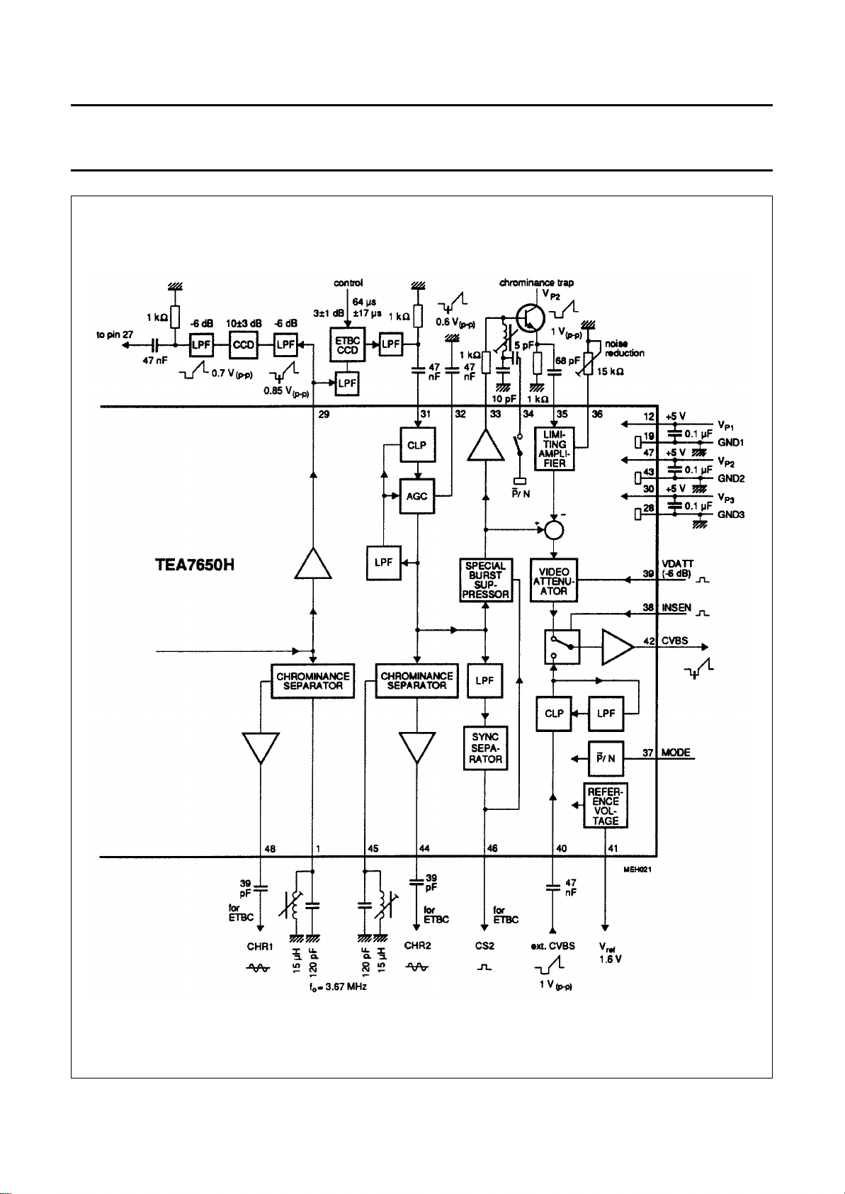
Fig.1 Block and test circuit; (continued in Fig.2)
Philips Semiconductors Preliminary specification
Video signal processor for CD-video/laser vision TEA7650H
September 1990 4
Fig.2 Block and test circuit; (continued from Fig.1).

Philips Semiconductors Preliminary specification
Video signal processor for CD-video/laser vision TEA7650H
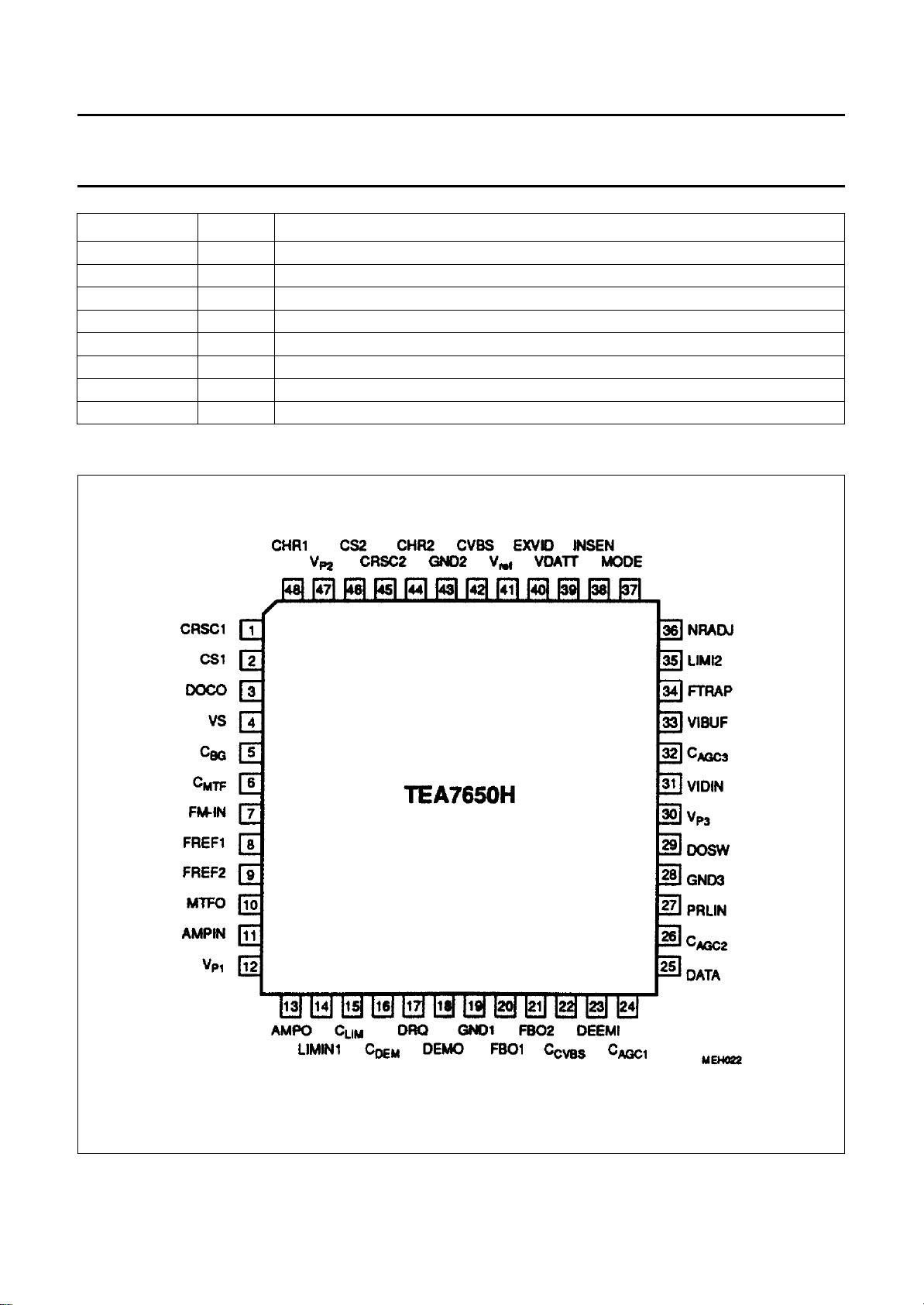
PINNING
SYMBOL PIN DESCRIPTION
CRSC1 1 3.67 MHz resonant circuit 1
CS1 2 line synchronization output pulse 1 (composite sync)
DOCO 3 drop out control, input/output for external control
VS 4 field sync output
C
BG
C
MTF
FM-IN 7 FM input signal from preamplifier
FREF1 8 PAL resonant circuit for the MTF
FREF2 9 NTSC resonant circuit for the MTF
MTFO 10 MTF output signal (corrected FM signal)
AMPIN 11 input for 8 dB amplifier (FM signal)
V
P1
AMPO 13 output of 8 dB amplifier (FM signal)
LIMIN1 14 limiter amplifier input (FM signal to demodulator)
C
LIM
C
DEM
DRQ 17 data request input for data at pin 25
DEMO 18 FM demodulator output (CVBS negative)
GND1 19 ground (0 V) for V
FBO1 20 feedback output at PAL and NTSC (de-emphasis)
FBO2 21 feedback output, additional at NTSC (de-emphasis)
C
CVBS
DEEMI 23 de-emphasis input for CVBS from demodulator
C
AGC1
DATA 25 data output of information code
C
AGC2
PRLIN 27 input signal of preceding line from CCD delay
GND3 28 ground (0 V) for V
DOSW 29 drop out switch buffer output (to CCD delay and ETBC)
V
P3
VIDIN 31 CVBS input signal from ETBC
C
AGC3
VIBUF 33 video signal buffer output to chroma trap circuitry
FTRAP 34 switching output for chroma trap at NTSC
LIMI2 35 limiter amplifier input for noise reduction
NRADJ 36 noise level adjust point (resistor to ground)
MODE 37 standard select input PAL/NTSC (PAL = LOW)
INSEN 38 insertion enable input
VDATT 39 6 dB CVBS attenuation (active HIGH)
EXVID 40 external CVBS input for insertion
5 charging capacitor for burst rectifier
6 charging capacitor for MTF control voltage
12 +5 V supply (referred to pins 6 to 15 and 18)
15 capacitor for slicing level control of limiter
16 capacitor for clamping level of FM demodulator
P1
22 capacitor for clamping of CVBS amplifier
24 capacitor for AGC of CVBS amplifier
26 capacitor for AGC of drop out amplifier
P3
30 +5 V supply (referred to pins 5, 17, 20 to 36, 38 to 42)
32 capacitor for AGC of CVBS follower amplifier
September 1990 5
Philips Semiconductors Preliminary specification
Video signal processor for CD-video/laser vision TEA7650H
SYMBOL PIN DESCRIPTION
V
ref
CVBS 42 main CVBS output signal
GND2 43 ground (0 V) for V
CHR2 44 chrominance output signal 2
CRSC2 45 3.67 MHz resonant circuit 2
CS2 46 line synchronization pulse 2 (composite sync)
V
P2
CHR1 48 chrominance output signal 1
PIN CONFIGURATION
41 reference voltage output (1.6 V)
P2
47 +5 V supply (referred to pins 1 to 4, 16, 37, 43 to 48)
September 1990 6
Fig.3 Pin configuration.

Philips Semiconductors Preliminary specification
Video signal processor for CD-video/laser vision TEA7650H
FUNCTIONAL DESCRIPTION
Figures 1, 2 show the block diagram of the Video Signal
Processor (VSP) including the peripheral circuitry for the
video signal processing. The pulse-width modulated FM
signal from the preamplifier is fed, via a DC blocking
capacitor, into the IC (pin 7) at the input to the Modulation
Transfer Function (MTF) circuit which corrects for the
characteristic of the optical reading system.
MTF correction
Due to the finite diameter of the laser beam spot and the
tangential velocity of the track of pits on the disk, the MTF
of the optical system acts like a radius-dependent
low-pass filter for the FM input signal. Although the video
signal can be recovered without correction, the ratio of the
amplitudes of the chrominance and luminance signals
would not then be the same at the most inner and the most
outer part of the disk. This influence of the disk radius is
automatically corrected by the Video Signal Processor.
The principle of correction is to use the deviation of the
demodulated burst signal to generate an error voltage in
order to control the frequency selective MTF circuit. The
burst measurement operates as follows: A burst-key
generator is triggered by the line synchronization pulse
(CS1) to generate a burst-key pulse which activates the
burst gate and rectifier stage. The signal at the rectifier
output (pin 6) is used to control the amplification of the
MTF circuit.
The carrier frequency in the PAL standard is different to
that in the NTSC standard, therefore two separate
resonant circuits are required on pins 8 and 9. They are
selected by the PAL/NTSC system selector (pin 37).
De-emphasis
The de-emphasis circuit consists of an internal inverting
amplifier and an external RC feedback network. Since the
pre-emphasis on the disk in the PAL standard is different
from that in the NTSC standard, the time constants are
switchable. When PAL is selected, the first arm of the
feedback network is active, otherwise both operate in
parallel. The de-emphasized video signal is fed into an
AGC stage (pin 20) where it is clamped on its black level
and amplitude-controlled to a constant level. The signal is
then fed into the data slicer and the drop out switch.
Data slicer
Coded signals on the video disk are extracted by the data
slicer (output pin 25) when the Data Request input is
activated (pin 17).
Drop out compensation
The drop out detector (DOD) in the IC is triggered by every
positive or negative transition of the FM signal. A drop out
is detected when the half-cycle period is outside the limits.
Protection against a drop out is achieved by use of a video
signal delayed by one line. The signal at the output of the
drop out switch is fed out of the IC via a buffer (pin 29) and
then through a delaying device (CCD) before being fed
back into the IC (pin 27). The delayed video signal appears
at the input of an AGC circuit to compensate for gain
tolerances of the delay line and avoids the need for an
external adjustment. When a drop out is detected, the drop
out detector activates the video switch so that the lost
information of the line is substituted by the information of
the preceding line.
The MTF-corrected FM signal at pin 10 is amplified (+8 dB)
and fed, via the external filter which removes the audio
frequency components from the signal, into the
demodulator at pin 14.
Demodulation
The FM signal is first fed into a limiter circuit (pin 14) with
automatic slicing level control to suppress the main carrier
in the demodulated signal. The demodulator has two
outputs. The first (internal) clamps the demodulated video
signal on peak-sync by controlling the transconductance of
the demodulator. The FM signal can now be demodulated
during disk start-up, thereby facilitating fast run-in. The
second output signal from the demodulator (pin 18) is
passed through an external 5 MHz low-pass filter to extract
the CVBS signal. The CVBS signal is then fed into the
de-emphasis network to compensate for the pre-emphasis
of the video signal recorded on the disk.
September 1990 7
The drop out pulse is also present at pin 3 and can be used
for different purposes. This pin can also act as an input to
control the drop out switch by an external signal for test
purposes.
Time error compensation
In a videodisc player timing errors are caused by
deviations of the rotational speed of the motor,
imperfections in the disk and unavoidable tolerances in the
centering of the disk on the turntable. Track eccentricity is
the main cause of timing errors.
To minimize timing errors, it is necessary in the first place
to keep the rotational speed of the disk as constant as
possible. Referring back to the output of the switch in
Fig.1-2, the video signal is also fed into a sync separator
and a chrominance separator with its external resonant
circuits tuned to the chrominance subcarrier
 Loading...