

Page 1
INTEGRATED CIRCUITS
DATA SH EET
TEA6886HL
Up-level Car radio Analog Signal
Processor (CASP)
Product specification
Supersedes data of 2000 Nov 21
2003 Feb 04
Page 2

Philips Semiconductors Product specification
Up-level Car radio Analog Signal
Processor (CASP)
CONTENTS
1 FEATURES
1.1 General
1.2 Stereo decoder and noise blanking
1.3 Weak signal processing
1.4 Audio pre-amplifier
2 GENERAL DESCRIPTION
3 ORDERING INFORMATION
4 QUICK REFERENCE DATA
5 BLOCK DIAGRAM
6 PINNING
7 FUNCTIONAL DESCRIPTION
7.1 Stereo decoder
7.2 FM noise blanker
7.3 AM noise blanker
7.4 Multipath/fading detection and weak signal
control
7.5 Tone/volume control
7.5.1 Source selector
7.5.2 Loudness
7.5.3 Volume 1
7.5.4 Treble
7.5.5 Bass
7.5.6 Volume 2
7.5.7 RSA selector
7.5.8 Chime adder
8 LIMITING VALUES
9 THERMAL CHARACTERISTICS
10 CHARACTERISTICS
11 I2C-BUS PROTOCOL
11.1 Read mode: 1st data byte
11.2 Read mode: 2nd data byte
11.3 Subaddress byte for write
11.4 Write mode: subaddress 0H
11.5 Write mode: subaddress 1H
11.6 Write mode: subaddress 2H
11.7 Write mode: subaddress 3H
11.8 Write mode: subaddress 4H
11.9 Write mode: subaddress 5H
11.10 Write mode: subaddress 6H
11.11 Write mode: subaddress 7H
11.12 Write mode: subaddress 8H
11.13 Write mode: subaddress 9H
11.14 Write mode: subaddress AH
11.15 Write mode: subaddress BH
11.16 Write mode: subaddress CH
TEA6886HL
12 INTERNAL CIRCUITRY
13 TEST CIRCUIT
14 PACKAGE OUTLINE
15 SOLDERING
15.1 Introduction to soldering surface mount
packages
15.2 Reflow soldering
15.3 Wave soldering
15.4 Manual soldering
15.5 Suitability of surface mount IC packages for
wave and reflow soldering methods
16 DATA SHEET STATUS
17 DEFINITIONS
18 DISCLAIMERS
19 PURCHASE OF PHILIPS I2C COMPONENTS
2003 Feb 04 2
Page 3

Philips Semiconductors Product specification
Up-level Car radio Analog Signal
Processor (CASP)
1 FEATURES
1.1 General
• I2C-bus compatible
• Digital alignment/adjustment via I2C-bus:
– FM noise blanker sensitivity
– FM stereo noise canceller
– FM High Cut Control (HCC)
– FM stereo separation.
• FM audio processing hold for RDS updating; holds the
detectors for the FM weak signal processing in their
present state
• FM bandwidth limiting; limits the bandwidth of the FM
audio signal with external capacitors
• AM stereo input; AM stereo audio can be fed in at the
pins for the de-emphasis capacitors; this will provide
8 dB of gain to the AM audio.
1.2 Stereo decoder and noise blanking
• FM stereo decoder
• Accepts FM multiplex signal and AM audio at input
• Pilot detector and pilot canceller
• De-emphasis selectable between 75 and 50 µs
• AM noise blanker: impulse noise detectorand an audio
hold.
1.3 Weak signal processing
TEA6886HL
• Volume 1 control from +20 to −56 dB in 1 dB steps;
programmable 20 dB loudness control included
• Volume 2 control from 0 to −56 dB in 1 dB steps,
−56, −58.5, −62, −68 dB and mute
• Programmable loudness control with bass boost as well
as bass and treble boost
• Treble control from −14 to +14 dB in 2 dB steps
• Bass control from −18 to +18 dB in 2 dB steps with
selectable characteristic
• Analog Step Interpolation (ASI) minimizes pops by
smoothing out the transitions in the audio signal when a
switch is made
• Audio Blend Control (ABC) minimizes pops by
automatically incrementing the volume and loudness
controls through each step between their present
settings and the new settings
• Rear Seat Audio (RSA) can select different sources for
the front and rear speakers
• Chime input: can be sent to any audio output, at any
volume level
• Chime adder circuit: chime input can also be summed
with left front and/or right front audio, or be turned off.
• FM weak signal processing: six signal condition
detectors, soft mute, stereo noise canceller (blend) and
high cut control (roll-off).
1.4 Audio pre-amplifier
• Source selector for 6 sources: 2 stereo inputs external
(A and B),1 symmetrical stereoinput(C),1 symmetrical
mono input (D), 1 internal stereo input (AM or FM) and
1 chime/diagnostic mono input
3 ORDERING INFORMATION
TYPE
NUMBER
TEA6886HL LQFP80 plastic low profile quad flat package; 80 leads; body 12 × 12 × 1.4 mm SOT315-1
2003 Feb 04 3
NAME DESCRIPTION VERSION
2 GENERAL DESCRIPTION
The TEA6886HL is a monolithic bipolar integrated circuit
providing the stereo decoder function and ignition noise
blanking facility combined with source selector and
tone/volume control for AM/FM car radio applications. The
device operates with a power supply voltage range from
7.8 to 9.2 V and a typical current consumption of 40 mA.
PACKAGE
Page 4

Philips Semiconductors Product specification
Up-level Car radio Analog Signal
TEA6886HL
Processor (CASP)
4 QUICK REFERENCE DATA
SYMBOL PARAMETER CONDITIONS MIN. TYP. MAX. UNIT
V
CC
I
CC
Stereo decoder path
S/N signal-to-noise ratio − 78 − dB
THD total harmonic distortion − 0.1 − %
α
cs
V
o(rms)
Tone/volume control
V
o(max)(rms)
G
v
G
step(vol)
G
bass
G
treble
G
step(treble, bass)
(S+N)/N signal-plus-noise to noise ratio Vo= 2.0 V; Gv= 0 dB;
THD total harmonic distortion V
RR
100
CMRR common mode rejection ratio
supply voltage 7.8 8.5 9.2 V
supply current 32 40 48 mA
channel separation 40 −−dB
output voltage level at pins ROPO
and LOPO (RMS value)
maximum output voltage level at
FM: 91% modulation;
840 950 1060 mV
AM: 100% modulation;
f
= 400 Hz
mod
VCC= 8.5 V; THD ≤ 0.1% 2000 −−mV
pins LF, LR, RF and RR (RMS value)
voltage gain 1 dB steps −112 − +20 dB
step resolution (volume) − 1 − dB
bass control −18 − +18 dB
treble control −14 − +14 dB
step resolution (bass and treble) − 2 − dB
− 107 − dB
unweighted
= 1.0 V; Gv=0dB − 0.01 − %
o(rms)
ripple rejection V
ripple(rms)
< 200 mV;
− 70 − dB
f = 100 Hz; Gv=0dB
48 53 − dB
differential stereo input
2003 Feb 04 4
Page 5
Philips Semiconductors Product specification
Up-level Car radio Analog Signal
Processor (CASP)
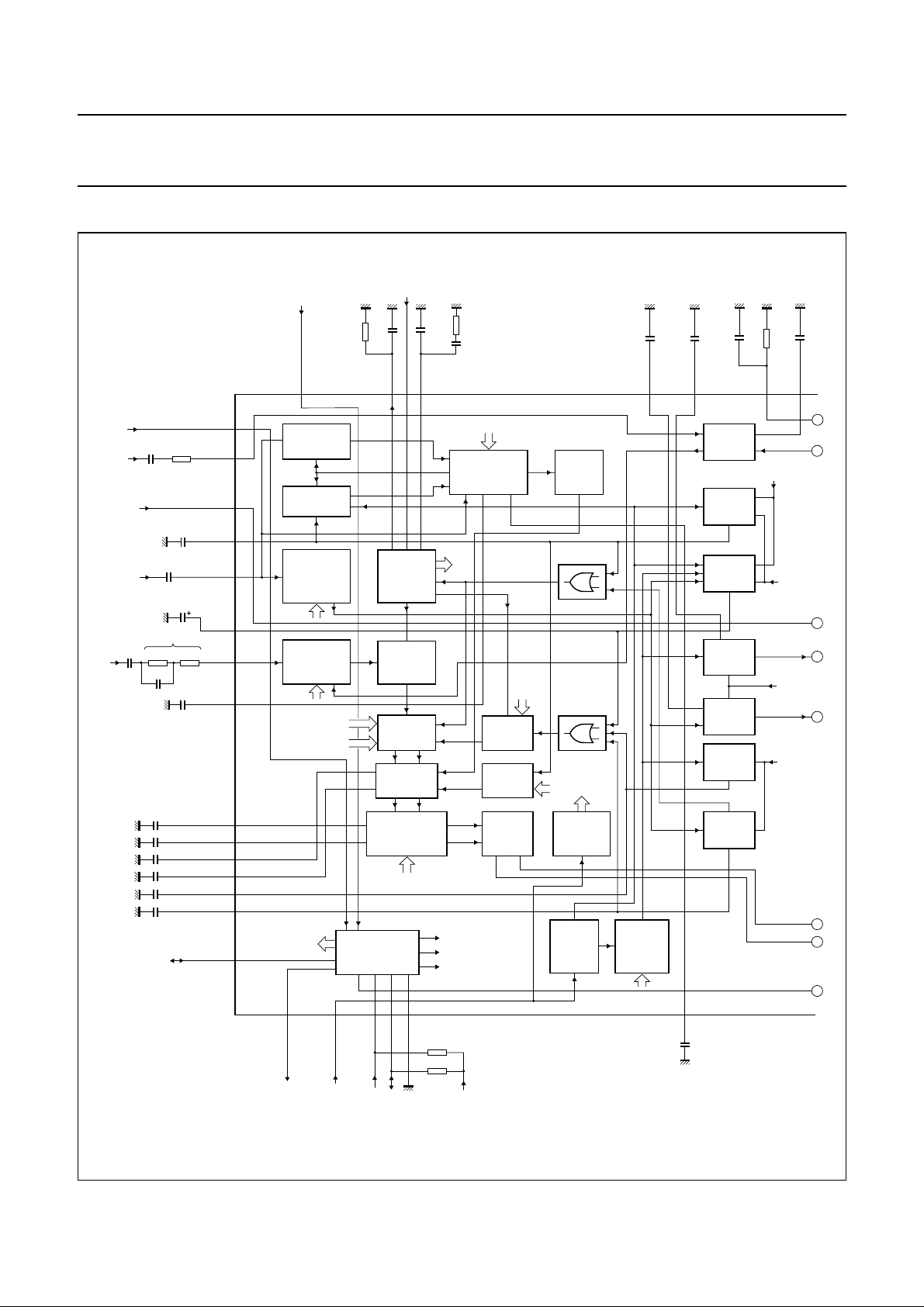
5 BLOCK DIAGRAM
handbook, full pagewidth
from
NICE
(FMHOLD)
33 nF
AM
mono
input
MPX
input
220
nF
RIN 182 kΩ
33 pF
2
C-bus
I
to NICE
220 kΩ
220 nF
10 nF
10 µF
10 nF
3.3 nF
3.3 nF
2.7 nF
2.7 nF
4.7 nF
4.7 nF
82 kΩ100 kΩ
FMHOLD
AMHIN
AMNBIN
TMUTE
MPXRDS
TSNC
MPXIN
FMNCAP
DEEML
DEEMR
FMLBUF
FMRBUF
TWBAM1
TUSN1
SDAQ
63
64
65
66
67
68
69
70
71
72
73
74
75
76
77
from
NICE
(AFSAMPLE)
470 kΩ
AFSAMPLE
59 58 57 56
120 kHz
HIGH-PASS
AMPLIFIER
AGC
PULSE
SEPARATOR
60 kHz
HIGH-PASS
AND
USN
DETECTOR
sensitivity
INPUT BUFFER
AND
80 kHz
LOW-PASS
sep.adj.
mute slope
mute start
bus controls
CONTROL LOGIC
2
I
C-bus
to NICE
3
SCLQ
level detector
4
LEVEL
from AM/FM
I2C-BUS
f
ref
(75.4 kHz)
100
nF
FM NB-GATES
DE-EMPHASIS
AM STEREO INPUT
AND
5
2
I
C-bus
10
68 kΩ
nF
100 nF
PILOT
FREF
PHASE
trigger sensitivity
NOISE
AND
INTERFERENCE
DETECTOR
pilot
STEREO
DECODER
PLL
V/I
CONVERTER
MATRIX
AND
SOFT-MUTE
FM BUFFER
AND
50/75 µs
AND
6
SCL
SDA
ind.
19 kHz
38 kHz
de-emphasis
switch
detector hold
detector reset
test
7 8
DGND
22 kΩ
22 kΩ
V
DD(5 V)
38 kHz
start/
slope
SNC
HCC
STEREO
DECODER
OUTPUT
FM
PULSE
FORMER
TEA6886HL
start/
slope
LEVEL
ADC
(6-BIT)
LEVEL
INPUT
BUFFER
BUS
sensitivity
20 kHz
BAND-PASS
AND
AMWB
DETECTOR
6.8 nF
TUSN2
55
TEA6886HL
100
6.8 nF
TWBAM2
54
AVERAGE
DETECTOR
(MUTE/HCC)
DETECTOR
DETECTOR
(WBAM2)
DETECTOR
AVERAGE
DETECTOR
(WBAM1)
AVERAGE
DETECTOR
TBL
10 nF
AM
GATE
PEAK
(SNC)
PEAK
PEAK
(USN2)
(USN1)
100
nF
kΩ
IREF
53
test
detector
hold
detector
reset
detector
hold
MHB818
22
nF
AMHCAP
52
A
B
C
D
E
F
G
H
Fig.1 Block diagram (continued in Fig.2).
2003 Feb 04 5
Page 6
Philips Semiconductors Product specification
Up-level Car radio Analog Signal
Processor (CASP)
handbook, full pagewidth
3.3
kΩ
330
10
pF
nF
AMHOLD
AMPCAP
LTC
51 50
A
B
AM
PULSE
FORMER
PEAK
TO
AVERAGE
DETECTOR
49
220
nF
LBI
48 47
220
nF
LBO
CHIME ADDER
(G = −20 dB)
AND
SWITCH
VOLUME 2
LEFT
FRONT
LF
46
BUS
15 nF
LR
ASICAP
45
44 43
BUS
BUS BUS
VOLUME 2
LEFT
REAR
BUS
REAR
SEAT
AUDIO
SWITCH
RR
BUS
VOLUME 2
RIGHT
REAR
CHIME ADDER
(G = −20 dB)
AND
SWITCH
BUS
VOLUME 2
RIGHT
FRONT
TEA6886HL
RF
37
220 nF
220 nF
10 nF
68 nF
C
KVR
100
C
VHS
47 µF
nF
100 nF
100 nF
1 µF
1 µF
3.3 kΩ
4.7 kΩ
43 kΩ
680 nF
220 nF
C
KIL
220 nF
C
KIR
220 nF
36
BUS
BUS
BUS
35
34
33
32
31
30
29
28
27
26
25
24
23
RBO
RBI
RTC
RLN
ROPI
ROPO
ALI
AMNCAP
ARI
VHS
MONOP
MONOC
CLIP
CCOM
MHB819
12
LLN
4.7 kΩ
43 kΩ
LEFT
BASS
BAND
LEFT
TREBLE
BAND
VOLUME 1
LEFT
LOUDNESS
LEFT
BUS
680 pF
LOPI
C
220 nF
KVL
ASI
ABC
INTERPOLATION
BLEND CONTROL
TEA6886HL
14
LOPO
ANALOG STEP
(ASI)
AUDIO
(ABC)
ASI/ABC
control
BUS
SOURCE SELECTOR
REAR SEAT AUDIO SELECTOR
16
1513
BRI
ADR
220nF
AND
17
BLI
220
nF
C
WBAM
INTERNAL
POWER
SUPPLY
V
CC
(+8.5 V)
ADC
(3-bit)
BUS
USN
ADC
(3-bit)
BUS
9
V
100 nF
10
CC
D
E
F
G
H
CHIME
11
AGND
68
nF
BUS
BUS
BUS
ASI
18
C
22 µF
ABC
SCAP
ELFI
RIGHT
BASS
BAND
RIGHT
TREBLE
BAND
VOLUME 1
RIGHT
LOUDNESS
RIGHT
BUS
19
CRIP
1 µF
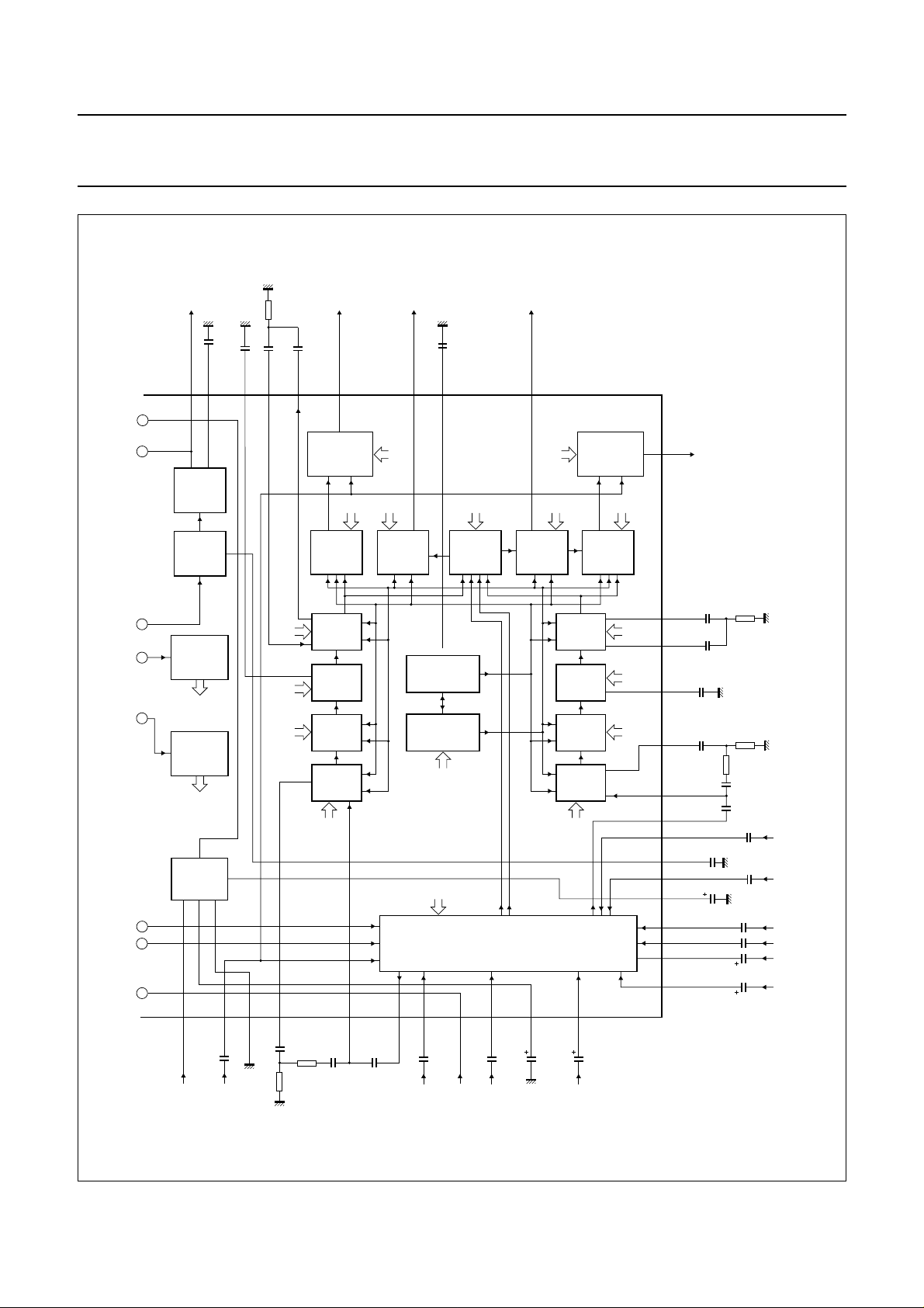
Fig.2 Block diagram (continued from Fig.1).
2003 Feb 04 6
Page 7

Philips Semiconductors Product specification
Up-level Car radio Analog Signal
TEA6886HL
Processor (CASP)
6 PINNING
SYMBOL PIN DESCRIPTION
n.c. 1 not connected
n.c. 2 not connected
SCLQ 3 clock output (to TEA6840H)
LEVEL 4 FM and AM level input (from TEA6840H)
SCL 5 I2C-bus clock input
SDA 6 I2C-bus data input/output
DGND 7 digital ground
TBL 8 time constant for FM modulation detector
V
CC
CHIME 10 chime tone input
AGND 11 analog ground
LLN 12 loudness left network
LOPI 13 left option port input (terminal impedance typical 100 kΩ)
LOPO 14 left option port output
BRI 15 channel B right stereo input (terminal impedance typical 100 kΩ)
ADR 16 address select input
BLI 17 channel B left stereo input (terminal impedance typical 100 kΩ)
SCAP 18 supply filter capacitor
CRIP 19 channel C right symmetrical input (terminal impedance typical 30 kΩ)
n.c. 20 not connected
n.c. 21 not connected
n.c. 22 not connected
CCOM 23 channel C common input (terminal impedance typical 30 kΩ)
CLIP 24 channel C left symmetrical input (terminal impedance typical 30 kΩ)
MONOC 25 mono common input (terminal impedance typical 30 kΩ)
MONOP 26 mono symmetrical input (terminal impedance typical 30 kΩ)
VHS 27 half supply filter capacitor
ARI 28 channel A right stereo input (terminal impedance typical 100 kΩ)
AMNCAP 29 peak-to-average detector capacitor for AM noise blanker
ALI 30 channel A left stereo input (terminal impedance typical 100 kΩ)
ROPO 31 right option port output
ROPI 32 right option port input (terminal impedance typical 100 kΩ)
RLN 33 loudness right network
RTC 34 right treble capacitor
RBI 35 right bass network input
RBO 36 right bass network output
RF 37 right front output
n.c. 38 not connected
n.c. 39 not connected
n.c. 40 not connected
9 supply voltage
2003 Feb 04 7
Page 8

Philips Semiconductors Product specification
Up-level Car radio Analog Signal
TEA6886HL
Processor (CASP)
SYMBOL PIN DESCRIPTION
n.c. 41 not connected
n.c. 42 not connected
RR 43 right rear output
ASICAP 44 analog step interpolate capacitor
LR 45 left rear output
LF 46 left front output
LBO 47 left bass network output
LBI 48 left bass network input
LTC 49 left treble capacitor
AMPCAP 50 AM blanking time capacitor
AMHOLD 51 AM noise blanker flag
AMHCAP 52 AM noise blanker hold capacitor
IREF 53 temperature independent reference current
TWBAM2 54 time constant for AM wideband peak detector
TUSN2 55 time constant for ultrasonic noise peak detector
PHASE 56 phase detector
FREF 57 frequency reference input (75.4 kHz from TEA6840H)
PILOT 58 pilot on/off output
AFSAMPLE 59 reset for multipath detector (from TEA6840H for RDS update)
n.c. 60 not connected
n.c. 61 not connected
n.c. 62 not connected
FMHOLD 63 FM audio processing hold input (from TEA6840H for RDS update)
AMHIN 64 AM signal input (from TEA6840H)
AMNBIN 65 AM noise blanker input (from TEA6840H)
TMUTE 66 time constant for soft mute
MPXRDS 67 unmuted MPX input (from TEA6840H for RDS update)
TSNC 68 time constant for stereo noise canceller
MPXIN 69 MPX input (from TEA6840H)
FMNCAP 70 FM noise detector capacitor
DEEML 71 left de-emphasis capacitor
DEEMR 72 right de-emphasis capacitor
FMLBUF 73 left AM/FM audio buffer capacitor
FMRBUF 74 right AM/FM audio buffer capacitor
TWBAM1 75 time constant for AM wideband average detector
TUSN1 76 time constant for ultrasonic noise average detector
SDAQ 77 data input/output (to TEA6840H)
n.c. 78 not connected
n.c. 79 not connected
n.c. 80 not connected
2003 Feb 04 8
Page 9

Philips Semiconductors Product specification
Up-level Car radio Analog Signal
Processor (CASP)
n.c.
n.c.
n.c.
SDAQ
TUSN1
TWBAM1
75
FMRBUF
74
handbook, full pagewidth
n.c.
n.c.
SCLQ
LEVEL
SCL
SDA
DGND
TBL
V
CC
CHIME
AGND
LLN
LOPI
LOPO
BRI
ADR
BLI
SCAP
CRIP
n.c.
80
79
78
77
76
1
2
3
4
5
6
7
8
9
10
11
12
13
14
15
16
17
18
19
20
FMLBUF
DEEMR
73
72
TEA6886HL
DEEML
71
FMNCAP
MPXIN
70
69
TSNC
68
MPXRDS
TMUTE
67
66
AMNBIN
AMHIN
65
64
TEA6886HL
FMHOLD
n.c.
n.c.
63
62
61
n.c.
60
AFSAMPLE
59
PILOT
58
FREF
57
PHASE
56
TUSN2
55
TWBAM2
54
IREF
53
AMHCAP
52
AMHOLD
51
AMPCAP
50
LTC
49
LBI
48
LBO
47
LF
46
LR
45
ASICAP
44
RR
43
n.c.
42
n.c.
41
21
22
23
24
25
26
27
28
29
n.c.
n.c.
CCOM
CLIP
MONOP
MONOC
VHS
ARI
AMNCAP
Fig.3 Pin configuration.
2003 Feb 04 9
30
ALI
31
ROPO
32
ROPI
33
RLN
34
RTC
35
RBI
36
RBO
37
RF
38
n.c.
39
n.c.
40
n.c.
MHB817
Page 10

Philips Semiconductors Product specification
Up-level Car radio Analog Signal
Processor (CASP)
7 FUNCTIONAL DESCRIPTION
7.1 Stereo decoder
The MPX input is the null-node of an operational amplifier
with internal feedback resistor. Adapting the stereo
decoder input to the level of the MPX signal, coming from
the FM demodulator output, is realized by the value of the
input series resistor RIN. To this input a second source
(AM detector output) can be fed by current addition.
The input amplifier is followed by an integrated 4th-order
Bessel low-pass filter with a cut-off frequency of 80 kHz.
It provides the necessary signal delay for FM noise
blanking and damping of high frequency interference at
the stereo decoder input.
The output signal of this filter is fed to the soft mute control
circuitry, the output is voltage-to-current converted and
then fed to the phase detector, pilot detector and pilot
canceller circuits, contained in the stereo decoder PLL
block. A PLL is used for regeneration of the 38 kHz
subcarrier. The fully integrated oscillator is adjusted by
means of a digital auxiliary PLL into the capture range of
the main PLL. The auxiliary PLL needs an external
reference frequency (75.4 kHz) which is provided by the
TEA6840H. The required 19 and 38 kHz signals are
generated by division of the oscillator output signal in a
logic circuit. The 19 kHz quadrature phase signal is fed to
the 19 kHz phase detector, where it is compared with the
incoming pilot tone. The DC output signal of the phase
detector controls the oscillator (PLL).
The pilot present detector is driven by an internally
generated in-phase 19 kHz signal. Its pilot dependent DC
output voltage is fed to a threshold switch, which activates
the pilot indicator bit and switches the stereo decoder to
stereo operation. The same DC voltage is used to control
theamplitudeofananti-phaseinternallygenerated 19 kHz
signal. The pilot tone is compensated by this anti-phase
19 kHz signal in the pilot canceller.
The pilot cancelled signal is fed to the matrix. There, the
side signal is demodulated and combined with the main
signal to the left and right audio channels. Compensation
for roll-off in the incoming MPX signal caused by the IF
filters and the FM demodulator is typically realized by an
external compensation network at pin MPXIN, individual
alignment is achieved by I2C-bus controlled amplification
of the side signal (DAA). A smooth mono-to-stereo
takeover is achieved by controlling the efficiency of the
matrix with the help of the SNC peak detector.
The matrix is followed by the FM noise suppression gates,
which are combined with FM single poles and High Cut
Control (HCC).
TEA6886HL
Thesinglepoleisdefinedbyinternal resistors and external
capacitors. Audio is fed from the gate circuits to the
switchable de-emphasis, where the demodulated AM
stereo signal can be fed in. After de-emphasis the signal
passes to the output buffers and is fed to the radio input of
the source selector. For HCC, the time constant of the
single pole contained in the output buffer can be changed
to higher values. This function is controlled by an average
detector contained in the multipath and fading detector.
7.2 FM noise blanker
The input of the ignition noise blanker is coupled to the
MPXRDS input signal and to the LEVEL input. Both
signalsarefedviaseparate120 kHz filters and rectifiers to
anaddercircuit.Theoutputsignalof the adder circuit is fed
in parallel to the noise detector and the interference
detector. The noise detector is a negative peak detector.
Its output controls the trigger sensitivity (prevention of
false triggering at noisy input signals) and the gain of the
MPX high-pass filter. The output of the interference
detector, when receiving a steep pulse, fires a single-shot
trigger circuit, contained in the pulse former circuitry. The
time constant of the single-shot trigger circuit is defined by
an internal capacitor, and its output activates the blanking
gates in the audio.
7.3 AM noise blanker
The AM noise blanking pulse is derived from the AM audio
signal which is fed into pin AMNBIN with the help of a
peak-to-averagecomparator. The blanking time is set by a
pulse former with external capacitor. The blanking pulse is
fed to the gate in the AM audio path and out at
pin AMHOLD to operate the gate built into the external
AM stereo processor.
7.4 Multipath/fading detection and weak signal
control
For FM signal quality dependent controls there is a built-in
combination of six detectors. These detectors are driven
by the level information direct, by the AC components on
thelevelviaa20 kHz band-pass filter (AM wideband) or by
the high notes present at the FM demodulator output via a
60 kHz high-pass filter (ultrasonic noise). The relationship
between the DC level and the AC components is
programmable by the I2C-bus (2 bits each). The output of
the level buffer, AM wideband detector and ultrasonic
noise detector are analog-to-digital converted and
readable by the I2C-bus.
2003 Feb 04 10
Page 11

Philips Semiconductors Product specification
Up-level Car radio Analog Signal
Processor (CASP)
For the period of fast RDS updating soft mute, SNC and
HCC can be put on hold. The AM wideband peak detector
and the ultrasonic noise peak detector are reset by a
switch signal delivered from the TEA6840H via pin
FMHOLD.
The six separate detecting circuits are as follows:
1. The AM wideband noise peak detector is driven from
a 20 kHz band-pass filter connected to the level buffer
output. The time constant is defined by an external
capacitor connected to pin TWBAM2. The output
voltage of the detector is analog-to-digital converted
by a 3-bit ADC.
2. The AM wideband noise average detector is driven
from a 20 kHz band-pass filter connected to the level
buffer output. The time constant is defined by an
external capacitor connected to pin TWBAM1. The
outputofthe detector is connected to the Stereo Noise
Control (SNC) circuit.
3. The ultrasonic noise peak detector is driven from a
60 kHz high-pass filter connected to the MPX signal
from pin MPXRDS. The time constant is defined by an
external capacitor connected to pin TUSN2. The
output voltage of the detector is analog-to-digital
converted by a 3-bit ADC.
4. The ultrasonic noise average detector is driven from a
60 kHz high-pass filter connected to the MPX signal
from pin MPXRDS. The time constant is defined by an
external capacitor connected to pin TUSN1. The
output of the detector is connected to soft mute control
and stereo noise control circuits.
5. For soft mute and high cut control purposes an
average detector with an externally defined time
constant (TMUTE) is provided. The detector is driven
byleveloutputonly.Softmuteandhighcutcontrolcan
be switched off via the I2C-bus.
6. The stereo noise control peak detector with an
externally defined time constant (TSNC) is driven by
DC level output, AM wideband and ultrasonic noise
outputs.Itprovidesthestereo blend facility (SNC).The
starting point and slope of the stereo blend can be
chosen via the I2C-bus controlled reference voltage.
TEA6886HL
7.5 Tone/volume control
The tone/volume control part consists of the following
functions:
• Source selector
• Loudness
• Volume 1
• Treble
• Bass
• Volume 2
• Rear Seat Audio (RSA) selector
• Chime adder
• Analog step interpolation
• Audio blend control.
The stages loudness, volume 1, bass and volume 2
include the Analog Step Interpolation (ASI) function. This
minimizes pops by smoothing out the transitions in the
audio signal during switching. The transition time is
I2C-bus programmable in a range of 1 : 24 in four steps.
The stages loudness, volume 1 and volume 2 also have
the Audio Blend Control (ABC) function. This minimizes
pops by automatically incrementing the volume and
loudnesscontrolsthrougheach step between theirpresent
settings and the new settings. The speed of the ABC
function is correlated with the transition time of the ASI
function.
All stages are controlled via the I2C-bus.
2003 Feb 04 11
Page 12

Philips Semiconductors Product specification
Up-level Car radio Analog Signal
Processor (CASP)
7.5.1 SOURCE SELECTOR
The source selector allows the selection between
6 sources:
• 2 external stereo inputs (ALI, ARI, BLI and BRI)
• 1 external symmetrical stereo input (CLIP, CRIP and
CCOM)
• 1 external symmetrical mono input (MONOP and
MONON)
• 1 internal stereo input (AM/FM)
• 1 chime/diagnostic mono input (CHIME).
A chime input signal can be sent to any audio output, at
any volume level, via the chime/diagnostic mono input.
7.5.2 LOUDNESS
The output of the source selector is fed into the loudness
circuitviatheexternalcapacitorC
and LOPI) and C
Depending on the external circuits for the left and the right
channel, only a bass boost or bass and treble boost is
available.Theexternalcircuits illustrated in Figs 13and 15
will produce the curves illustrated in Figs 14 and 16
(without the influence of C
(between pins ROPO and ROPI).
KVR
and C
KVL
(betweenpinsLOPO
KVL
respectively).
KVR
TEA6886HL
7.5.5 BASS
Thebasscontrolisthenext stage. The characteristic ofthe
bass curves depends upon the external circuits connected
to pins LBO and LBI (left channel) and pins RBO and RBI
(rightchannel)andalsouponthe setting of bit BSYM(MSB
of the bass control byte). When BSYM = 1, an equalizer
characteristic is obtained and when BSYM = 0, a shelving
characteristic is obtained.
Figures 17 and 18 show the bass curves with an external
circuit of 2 × 220 nF capacitors and a resistor of 3.3 kΩ for
each channel with different values for BSYM. Figure 19
shows the bass curves with an external capacitor of 47 nF
for each channel and BSYM = 0, for boost and cut.
7.5.6 VOLUME 2
The four volume 2 blocks are located at the end of the
tone/volume control. In addition to volume control (same
settings as volume 2) the balance and fader functions are
alsoperformedbyindividualattenuation offsets for the four
attenuators. The control range of these attenuators is
56 dB in steps of 1 dB and the additional steps of
−58.5 dB, −62 dB, −68 dB and a mute step.
7.5.7 RSA SELECTOR
7.5.3 VOLUME 1
The volume 1 control circuit follows the loudness circuit.
The control range of volume 1 is between +20 and −36 dB
in steps of 1 dB.
7.5.4 TREBLE
The output signal of the volume 1 control circuit is fed into
the treble control stage. The control range is between
+14 and −14 dB in steps of 2 dB. Fig.20 shows the control
characteristic with external capacitors of 10 nF.
The RSA selector provides the possibility to select an
alternative source for the rear channels. In this event rear
channels are only controlled by the volume 2 function.
7.5.8 CHIME ADDER
The chime adder circuit enables the chime input signal to
be summed with the left front and/or right front audio, or be
turned off.
2003 Feb 04 12
Page 13
Philips Semiconductors Product specification
Up-level Car radio Analog Signal
TEA6886HL
Processor (CASP)
8 LIMITING VALUES
In accordance with the Absolute Maximum Rating System (IEC 60134).
SYMBOL PARAMETER CONDITIONS MIN. MAX. UNIT
V
CC
V
i
P
tot
T
stg
T
amb
V
es
Notes
1. Machine model (R = 0 Ω, C = 200 pF).
2. Human body model (R = 1.5 kΩ, C = 100 pF).
9 THERMAL CHARACTERISTICS
supply voltage −0.3 +10 V
voltage at all pins (except SCL and SDA) VCC≤ 10 V VSS− 0.3 V
CC
voltage at pins SCL and SDA VSS− 0.3 9.7 V
total power dissipation − 480 mW
storage temperature −65 +150 °C
ambient temperature −40 +85 °C
electrostatic handling voltage for all pins note 1 −200 +200 V
note 2 −2000 +2000 V
V
SYMBOL PARAMETER CONDITIONS VALUE UNIT
R
th(j-a)
thermal resistance from junction to ambient in free air 54 K/W
2003 Feb 04 13
Page 14

This text is here in white to force landscape pages to be rotated correctly when browsing through the pdf in the Acrobat reader.This text is here in
_white to force landscape pages to be rotated correctly when browsing through the pdf in the Acrobat reader.This text is here inThis text is here in
white to force landscape pages to be rotated correctly when browsing through the pdf in the Acrobat reader. white to force landscape pages to be ...
2003 Feb 04 14
10 CHARACTERISTICS
FM part: input signal V
i(MPX)(p-p)
= 1.89 V; m = 100% (∆f=±75 kHz, f
= 400 Hz); de-emphasis of 75 µs and series resistor at input RIN= 182 kΩ;
mod
FM audio measurements are taken at pins LOPO and ROPO.
Tone part: R
= 600 Ω; RL=10kΩ, AC-coupled; CL= 2.5 nF; CLK = square wave (5 to 0 V) at 100 kHz; stereo source = A channel input; volume 1
S
attenuator = 0 dB; loudness=0dB, off; volume 2 attenuators = 0 dB; bass linear; treble linear; input voltage = 1 V, f = 1 kHz. Tone part audio
measurements are taken at pins RF and LF. V
= 8.3 to 8.7 V; VSS=0V; T
CC
=25°C; unless otherwise specified.
amb
This IC shall not radiate noise in the audio system such that it disturbs any other circuit. This IC shall also not be susceptible to the radiation of any
other circuit.
SYMBOL PARAMETER CONDITIONS MIN. TYP. MAX. UNIT
V
I
CC
V
I
IREF
CC
HS
supply voltage 7.8 8.5 9.2 V
supply current VCC=8.5V 324048mA
half supply voltage VCC= 8.5 V 3.75 4.25 4.75 V
reference current VCC= 8.5 V; R
= 100 kΩ 35 37 39 µA
IREF
FM signal path
V
i(MPX)(p-p)
∆V
i(MPX)
I
i
I
i(max)
V
o(rms)
∆V
out
α
cs
MPX input signal (peak-to-peak value) Ri= 182 kΩ−1.89 − V
overdrive margin of MPX input signal THD = 1% 6 −−dB
AF input current − 3.66 −µA
maximum AF input current THD = 1% 7.32 −−µA
AF mono output signal (RMS value) 91% modulation without pilot 890 1000 1110 mV
AF mono channel balance without pilot; V
LOPO/VROPO
−1 − +1 dB
channel separation aligned setting of data byte 1, bit 0 to bit 3;
m = 30% modulation plus 9% pilot
L=1; R=0 404770dB
L=0; R=1 404770dB
THD total harmonic distortion V
i(MPX)(p-p)
V
i(MPX)(p-p)
= 1.89 V; f
= 1.89 V; f
= 1 kHz without pilot − 0.1 0.3 %
mod
= 5 kHz
mod
L=1; R=0 − 0.1 0.3 %
L=0; R=1 − 0.1 0.3 %
S/N signal-to-noise ratio f = 20 Hz to 15 kHz 75 78 − dB
α
19
α
38
α
57
α
76
pilot signal suppression f = 19 kHz 40 50 − dB
subcarrier suppression f = 38 kHz 35 50 − dB
f = 57 kHz 40 −−dB
f = 76 kHz 50 60 − dB
Philips Semiconductors Product specification
Up-level Car radio Analog Signal
Processor (CASP)
TEA6886HL
Page 15

This text is here in white to force landscape pages to be rotated correctly when browsing through the pdf in the Acrobat reader.This text is here in
_white to force landscape pages to be rotated correctly when browsing through the pdf in the Acrobat reader.This text is here inThis text is here in
white to force landscape pages to be rotated correctly when browsing through the pdf in the Acrobat reader. white to force landscape pages to be ...
2003 Feb 04 15
SYMBOL PARAMETER CONDITIONS MIN. TYP. MAX. UNIT
IM2 second order intermodulation for
f
= 1 kHz
spur
IM3 third order intermodulation for f
α
57(RDS)
α
67
traffic radio (RDS) f = 57 kHz; note 2 − 70 − dB
Subsidiary Communication Authorization
= 1 kHz f
spur
f
= 10 kHz; note 1 − 60 − dB
mod
= 13 kHz; note 1 − 58 − dB
mod
f = 67 kHz; note 3 70 −−dB
(SCA)
α
114
α
190
PSRR power supply ripple rejection f = 100 Hz; V
R
R
I
FMLBUF
I
FMRBUF
SDEEML
SDEEMR
;
;
Adjacent Channel Interference (ACI) f = 114 kHz; note 4 − 80 − dB
f = 190 kHz; note 4 − 70 − dB
ripple(rms)
= 100 mV − 30 − dB
de-emphasis output source resistance data byte 3, bit 5 = 1; 75 µs 20 22.7 25.4 kΩ
data byte 3, bit 5 = 0; 50 µs 13.4 15.2 17 kΩ
current capacity of FM buffer V
FMLBUF,FMRBUF
= 5.5 ±1V 50 − 200 µA
PLL VCO
f
osc
oscillator frequency − 228 − kHz
frequency range of free running oscillator 190 − 270 kHz
f
ref
V
i(FREF)
Z
i(FREF)
reference frequency at pin FREF − 75.4 − kHz
reference frequency input voltage 30 100 500 mV
input impedance 100 −−kΩ
PLL pilot detector
V
i(pilot)(rms)
hys
(pilot)
V
PILOT
pilot threshold voltage for automatic
switching by pilot input voltage (RMS value)
stereo on; STIN = 1 − 27 37 mV
stereo off; STIN = 0 9 22 − mV
hysteresis of pilot threshold voltage − 2 − dB
switching voltage for external mono control
0.3 − 0.7 V
(PILOT)
AM signal path
V
G
LOPO
v
; V
ROPO
AC output voltage at pins LOPO
and ROPO
AMON = 1 and AMST = 0; Ri= 220 kΩ;
V
iAM(mono)
= 250 mV
AM stereo audio buffer voltage gain subaddress 0H: AMON = 1 and AMST = 1; input
195 245 295 mV
789dB
signal at pins DEEML or DEEMR; coupled with
R
i(DEEML);
R
i(DEEMR)
220 nF; V
i(DEEML,DEEMR)
input resistance for AM stereo left and right AMON = 1 and AMST = 1; note 6 80 100 120 kΩ
= 200 mV; fi= 1 kHz; note 5
Philips Semiconductors Product specification
Up-level Car radio Analog Signal
Processor (CASP)
TEA6886HL
Page 16

This text is here in white to force landscape pages to be rotated correctly when browsing through the pdf in the Acrobat reader.This text is here in
_white to force landscape pages to be rotated correctly when browsing through the pdf in the Acrobat reader.This text is here inThis text is here in
white to force landscape pages to be rotated correctly when browsing through the pdf in the Acrobat reader. white to force landscape pages to be ...
2003 Feb 04 16
SYMBOL PARAMETER CONDITIONS MIN. TYP. MAX. UNIT
Noise blanker
FM PART
t
sup
I
offset
interference suppression time 20 30 40 µs
gate input offset current at pins during
during AF suppression time − 20 50 nA
suppression pulse duration
I
ch(FMNCAP)
I
dch(FMNCAP)
charge current (into 4 V) no input signal; V
discharge current (from 5.5 V) no input signal; V
FMNCAP=VFMNCAP(int)
FMNCAP=VFMNCAP(int)
− 0.7 V −16 −12.5 −9.5 µA
+ 0.7 V 45 70 100 µA
Trigger Threshold Control (TTC), dependency on MPX signal at MPXRDS input
V
FMNCAP
∆V
FMNCAP
∆V
TBL
trigger threshold variation voltage V
trigger threshold voltage V
trigger threshold variation with audio
i(MPXRDS)
i(MPXRDS)
V
i(MPXRDS)
V
i(MPXRDS)
= 0 V 4.5 5 5.5 V
= 10 mV; f = 120 kHz 15 40 80 mV
= 100 mV; f = 120 kHz 75 100 200 mV
= 670 mV − 500 − mV
frequency f = 15 kHz
Trigger Threshold Control (TTC), dependency on level detector input signal
V
FMNCAP
∆V
FMNCAP
trigger threshold voltage V
trigger threshold voltage as a function of
V
LEVEL(AC)
LEVEL(AC)
V
LEVEL(AC)
V
LEVEL(AC)
= 0 V 4.5 5 5.5 V
= 10 mV; f = 120 kHz − 0 − mV
= 200 mV; f = 120 kHz − 40 − mV
Trigger sensitivity measurement with pulse (on MPX signal) at MPXRDS input
V
pulse
trigger sensitivity t
=10µs; write mode; data byte 3, bits 6 and 7:
pulse
NBS1 = 0; NBS0 = 0 − 60 − mV
NBS1 = 0; NBS0 = 1 − 100 − mV
NBS1 = 1; NBS0 = 0 − 150 − mV
NBS1 = 1; NBS0 = 1 − 200 − mV
Trigger sensitivity measurement with pulse (on level signal) at AM/FM level input
V
pulse
trigger sensitivity t
pulse
=10µs; V
= 0.5 V; write mode;
LEVEL
data byte 3, bits 6 and 7:
NBS1 = 0; NBS0 = 0 − 250 − mV
NBS1 = 0; NBS0 = 1 − 275 − mV
NBS1 = 1; NBS0 = 0 − 300 − mV
NBS1 = 1; NBS0 = 1 − 320 − mV
Philips Semiconductors Product specification
Up-level Car radio Analog Signal
Processor (CASP)
TEA6886HL
Page 17

This text is here in white to force landscape pages to be rotated correctly when browsing through the pdf in the Acrobat reader.This text is here in
_white to force landscape pages to be rotated correctly when browsing through the pdf in the Acrobat reader.This text is here inThis text is here in
white to force landscape pages to be rotated correctly when browsing through the pdf in the Acrobat reader. white to force landscape pages to be ...
2003 Feb 04 17
SYMBOL PARAMETER CONDITIONS MIN. TYP. MAX. UNIT
AM PART
m
mod
V
AMPCAP(AC)
α
AMGATE
t
sup(AMHOLD)
V
AMNCAP(DC)
f
AMHOLD
I
offset
trigger threshold − 140 − %
AF voltage at AMHCAP V
attenuation of blanking gate V
suppression time at AMHOLD t
detector voltage; V
ext(AMNBIN)DC
− 0.7 V V
trigger sensitivity t
gate input offset current at pins during
iAM(mono)
iAM(mono)
voltage; gate closed: V
pulse
(AMNBIN); V
AMNBIN(AC)
pulse
(AMNBIN); V
during AF suppression time −50 0 +50 nA
= 50 mV (RMS); f=1kHz 16 22 30 mV
= 50 mV (RMS); gate open: internal
AMHOLD(DC)
= 4 V; note 7
=10µs; repetition rate = 50 Hz; V
= 0.5 V
LEVEL
=0V; V
LEVEL(DC)
= 3.5 V 3 3.5 4 V
=10µs; repetition rate = 50 Hz; V
=4V
LEVEL
pulse
pulse
= 1.7 V
= 1.7 V
−60 −70 −80 dB
400 500 600 µs
45 50 55 Hz
suppression pulse duration
Muting average detector (TMUTE); see Fig.12
V
i(LEVEL)
G
v
∆V
TMUTE
∆V
TMUTE/K
input voltage on LEVEL 0.5 − 4V
voltage gain LEVEL to TMUTE − 0 − dB
offset between TMUTE and LEVEL − 1.5 − V
temperature dependence at TMUTE − 3.3 − mV/K
MUTING AVERAGE DETECTOR TIME CONSTANT
I
ch(TMUTE)
I
dch(TMUTE)
V
O
TMUTE charge current −−0.2 −µA
TMUTE discharge current − 0.2 −µA
DC output voltage 2 − 5V
TEST CONDITION
I
ch(test)
I
dch(test)
capacitor charge current data byte 6, bit7=1 −−12 −µA
capacitor discharge current data byte 6, bit7=1 − 12 −µA
Philips Semiconductors Product specification
Up-level Car radio Analog Signal
Processor (CASP)
TEA6886HL
Page 18

This text is here in white to force landscape pages to be rotated correctly when browsing through the pdf in the Acrobat reader.This text is here in
_white to force landscape pages to be rotated correctly when browsing through the pdf in the Acrobat reader.This text is here inThis text is here in
white to force landscape pages to be rotated correctly when browsing through the pdf in the Acrobat reader. white to force landscape pages to be ...
2003 Feb 04 18
SYMBOL PARAMETER CONDITIONS MIN. TYP. MAX. UNIT
AM wideband average detector (TWBAM1); see Fig.6
V
TWBAM1
DC voltage at TWBAM1 with respect to
AGND
V
LEVEL(AC)
= 400 mV;V
LEVEL(DC)
= 3.5 V;fi= 24 kHz;
write mode; data byte 1, bits 4 and 5:
AWS1 = 1; AWS0 = 1 − 4.10 − V
AWS1 = 1; AWS0 = 0 − 3.60 − V
AWS1 = 0; AWS0 = 1 − 3.00 − V
AWS1 = 0; AWS0 = 0 − 2.35 − V
VC
TWBAM1
DC voltage coefficient V
LEVEL(AC)
= 400 mV;V
LEVEL(DC)
= 3.5 V;fi= 24 kHz;
write mode; note 8; data byte 1, bits 4 and 5:
AWS1 = 1; AWS0 = 1 0.69 0.82 0.98
AWS1 = 1; AWS0 = 0 0.60 0.72 0.86
AWS1 = 0; AWS0 = 1 0.50 0.60 0.71
AWS1 = 0; AWS0 = 0 0.40 0.47 0.56
V
O
DC output voltage 1.5 − 5.5 V
AM WIDEBAND AVERAGE DETECTOR TIME CONSTANT
I
ch(TWBAM1)
I
dch(TWBAM1)
TWBAM1 charge current −19.5 −15 −11.5 µA
TWBAM1 discharge current 11.5 15 19.5 µA
Ultrasonic noise average detector (TUSN1); see Fig.5
V
TUSN1
DC voltage at TUSN1 with respect to
AGND
V
MPXRDS(AC)
= 350 mV; V
LEVEL(DC)
= 3.5 V;
fi= 80 kHz; write mode; data byte 1, bits 6 and 7:
USS1 = 1; USS0 = 1 − 4.25 − V
USS1 = 1; USS0 = 0 − 4.00 − V
USS1 = 0; USS0 = 1 − 3.50 − V
USS1 = 0; USS0 = 0 − 2.60 − V
VC
TUSN1
DC voltage coefficient V
MPXRDS(AC)
= 350 mV; V
LEVEL(DC)
= 3.5 V;
fi= 80 kHz; write mode; note 9; data byte 1,
bits 6 and 7:
USS1 = 1; USS0 = 1 0.71 0.85 1.00
USS1 = 1; USS0 = 0 0.67 0.80 0.95
USS1 = 0; USS0 = 1 0.60 0.70 0.85
USS1 = 0; USS0 = 0 0.44 0.52 0.62
V
O
DC output voltage 1.5 − 5.5 V
Philips Semiconductors Product specification
Up-level Car radio Analog Signal
Processor (CASP)
TEA6886HL
Page 19

This text is here in white to force landscape pages to be rotated correctly when browsing through the pdf in the Acrobat reader.This text is here in
_white to force landscape pages to be rotated correctly when browsing through the pdf in the Acrobat reader.This text is here inThis text is here in
white to force landscape pages to be rotated correctly when browsing through the pdf in the Acrobat reader. white to force landscape pages to be ...
2003 Feb 04 19
SYMBOL PARAMETER CONDITIONS MIN. TYP. MAX. UNIT
ULTRASONIC NOISE AVERAGE DETECTOR TIME CONSTANT
I
ch(TUSN1)
I
dch(TUSN1)
TUSN1 charge current −19.5 −15 −11.5 µA
TUSN1 discharge current 11.5 15 19.5 µA
Peak detector for stereo noise control (TSNC)
DEPENDENCY ON LEVEL VOLTAGE; see Fig.12
V
LEVEL
input voltage 0.5 − 4.75 V
G gain LEVEL to TSNC − 0 − dB
V
∆V
TSNC
TSNC/K
DC voltage at TSNC referred to DC level
voltage at LEVEL
without MPXRDS and LEVEL (AC) input
V
LEVEL(DC)
V
LEVEL(DC)
= 0.5 V 1.75 2.00 2.25 V
= 3.5 V 4.50 5.00 5.50 V
temperature dependence at TSNC − 3.3 − mV/K
DEPENDENCY ON ULTRASONIC NOISE; see Fig.5
V
TSNC
DC voltage at TSNC with respect to AGND V
MPXRDS(AC)
= 350 mV; V
LEVEL(DC)
= 3.5 V;
fi= 80 kHz; write mode; data byte 1, bits 6 and 7:
USS1 = 1; USS0 = 1 − 4.25 − V
USS1 = 1; USS0 = 0 − 4.00 − V
USS1 = 0; USS0 = 1 − 3.50 − V
USS1 = 0; USS0 = 0 − 2.60 − V
VC
TSNC
DC voltage coefficient V
MPXRDS(AC)
= 350 mV; V
LEVEL(DC)
= 3.5 V;
fi= 80 kHz; write mode; note 10; data byte 1,
bits 6 and 7:
USS1 = 1; USS0 = 1 0.71 0.85 1.00
USS1 = 1; USS0 = 0 0.67 0.80 0.95
USS1 = 0; USS0 = 1 0.60 0.70 0.85
USS1 = 0; USS0 = 0 0.44 0.52 0.62
V
O
DC output voltage 2 − 5V
Philips Semiconductors Product specification
Up-level Car radio Analog Signal
Processor (CASP)
TEA6886HL
Page 20

This text is here in white to force landscape pages to be rotated correctly when browsing through the pdf in the Acrobat reader.This text is here in
_white to force landscape pages to be rotated correctly when browsing through the pdf in the Acrobat reader.This text is here inThis text is here in
white to force landscape pages to be rotated correctly when browsing through the pdf in the Acrobat reader. white to force landscape pages to be ...
2003 Feb 04 20
SYMBOL PARAMETER CONDITIONS MIN. TYP. MAX. UNIT
DEPENDENCY ON AM WIDEBAND NOISE; see Fig.6
V
TSNC
DC voltage at TSNC V
LEVEL(AC)
= 400 mV;V
LEVEL(DC)
= 3.5 V;fi= 24 kHz;
write mode; data byte 1, bits 4 and 5:
AWS1 = 1; AWS0 = 1 − 4.10 − V
AWS1 = 1; AWS0 = 0 − 3.60 − V
AWS1 = 0; AWS0 = 1 − 3.00 − V
AWS1 = 0; AWS0 = 0 − 2.35 − V
VC
TSNC
DC voltage coefficient V
LEVEL(AC)
= 400 mV;V
LEVEL(DC)
= 3.5 V;fi= 24 kHz;
write mode; note 11; data byte 1, bits 4 and 5:
AWS1 = 1; AWS0 = 1 0.69 0.82 0.98
AWS1 = 1; AWS0 = 0 0.60 0.72 0.86
AWS1 = 0; AWS0 = 1 0.50 0.60 0.71
AWS1 = 0; AWS0 = 0 0.40 0.47 0.56
V
O
DC output voltage 1.5 − 5.5 V
DETECTOR TIME CONSTANT
I
ch(TSNC)
I
dch(TSNC)
TSNC charge current −−2.5 −µA
TSNC discharge current − 65 −µA
TEST CONDITION
I
ch(test)
I
dch(test)
charge current for testing data byte 6, bit 7 = 1; V
V
TSNC(DC)
= 2.8 V
discharge current for testing data byte 6, bit 7 = 1; V
V
TSNC(DC)
= 4.2 V
LEVEL(DC)
LEVEL(DC)
=2V;
=2V;
−−1.5 − mA
− 200 −µA
Philips Semiconductors Product specification
Up-level Car radio Analog Signal
Processor (CASP)
TEA6886HL
Page 21

This text is here in white to force landscape pages to be rotated correctly when browsing through the pdf in the Acrobat reader.This text is here in
_white to force landscape pages to be rotated correctly when browsing through the pdf in the Acrobat reader.This text is here inThis text is here in
white to force landscape pages to be rotated correctly when browsing through the pdf in the Acrobat reader. white to force landscape pages to be ...
2003 Feb 04 21
SYMBOL PARAMETER CONDITIONS MIN. TYP. MAX. UNIT
Ultrasonic noise peak detector (TUSN2); see Fig.5
V
TUSN2
DC voltage at TUSN2 with respect to
AGND
V
MPXRDS(AC)
= 350 mV; V
LEVEL(DC)
= 3.5 V;
fi= 80 kHz; write mode; data byte 1, bits 6 and 7:
USS1 = 1; USS0 = 1 − 4.25 − V
USS1 = 1; USS0 = 0 − 4.00 − V
USS1 = 0; USS0 = 1 − 3.50 − V
USS1 = 0; USS0 = 0 − 2.60 − V
VC
TUSN2
DC voltage coefficient V
MPXRDS(AC)
= 350 mV; V
LEVEL(DC)
= 3.5 V;
fi= 80 kHz; write mode; note 12; data byte 1,
bits 6 and 7:
USS1 = 1; USS0 = 1 0.71 0.85 1.00
USS1 = 1; USS0 = 0 0.67 0.80 0.95
USS1 = 0; USS0 = 1 0.60 0.70 0.85
USS1 = 0; USS0 = 0 0.44 0.52 0.62
V
O
DC output voltage 1.5 − 5.5 V
DETECTOR TIME CONSTANT
I
ch(TUSN2)
I
dch(TUSN2)
TUSN2 charge current −−1.6 −µA
TUSN2 discharge current − 21 −µA
AM wideband peak detector (TWBAM2); see Fig.6
V
TWBAM2
DC voltage at TWBAM2 with respect to
AGND
V
LEVEL(AC)
= 400 mV;V
LEVEL(DC)
= 3.5 V;fi= 24 kHz;
write mode; data byte 1, bits 4 and 5:
AWS1 = 1; AWS0 = 1 − 4.10 − V
AWS1 = 1; AWS0 = 0 − 3.60 − V
AWS1 = 0; AWS0 = 1 − 3.00 − V
AWS1 = 0; AWS0 = 0 − 2.35 − V
VC
TWBAM2
DC voltage coefficient V
LEVEL(AC)
= 400 mV;V
LEVEL(DC)
= 3.5 V;fi= 24 kHz;
write mode; note 13; data byte 1, bits 4 and 5:
AWS1 = 1; AWS0 = 1 0.69 0.82 0.98
AWS1 = 1; AWS0 = 0 0.60 0.72 0.86
AWS1 = 0; AWS0 = 1 0.50 0.60 0.71
AWS1 = 0; AWS0 = 0 0.40 0.47 0.56
V
O
DC output voltage 2 − 5V
Philips Semiconductors Product specification
Up-level Car radio Analog Signal
Processor (CASP)
TEA6886HL
Page 22

This text is here in white to force landscape pages to be rotated correctly when browsing through the pdf in the Acrobat reader.This text is here in
_white to force landscape pages to be rotated correctly when browsing through the pdf in the Acrobat reader.This text is here inThis text is here in
white to force landscape pages to be rotated correctly when browsing through the pdf in the Acrobat reader. white to force landscape pages to be ...
2003 Feb 04 22
SYMBOL PARAMETER CONDITIONS MIN. TYP. MAX. UNIT
DETECTOR TIME CONSTANT
I
ch(TWBAM2
I
dch(TWBAM2)
) TWBAM2 charge current −−1.6 −µA
TWBAM2 discharge current − 21 −µA
Soft mute; see Figs 7 and 4
α
0dB
α
6dB
attenuation at LOPO and ROPO V
start of muting; AC attenuation at
LOPO and ROPO
TMUTE
= 3.5 V; V
= 3.5 V −0.5 0 +0.5 dB
TUSN1
see Fig.4; write mode; MSL0 = 1; MSL1 = 1
MST1 = 0; MST0 = 0; V
TMUTE
= 0.42V
TUSN1
369dB
without AC
MST1 = 0; MST0 = 1; V
TMUTE
= 0.45V
TUSN1
369dB
without AC
MST1 = 1; MST0 = 0; V
TMUTE
= 0.47V
TUSN1
369dB
without AC
MST1 = 1; MST0 = 1; V
TMUTE
= 0.49V
TUSN1
369dB
without AC
α
10dB
AC attenuation for setting of mute slope at
LOPO and ROPO
MST1 = 0; MST0 = 0; see Fig.7
MSL1 = 0; MSL0 = 0; V
TMUTE(DC)
= 0.35V
TUSN1
7 1013dB
without AC
MSL1 = 0; MSL0 = 1; V
TMUTE(DC)
= 0.38V
TUSN1
7 1013dB
without AC
MSL1 = 1; MSL0 = 0; V
TMUTE(DC)
= 0.39V
TUSN1
7 1013dB
without AC
MSL1 = 1; MSL0 = 1; V
TMUTE(DC)
= 0.395V
TUSN1
7 1013dB
without AC
Philips Semiconductors Product specification
Up-level Car radio Analog Signal
Processor (CASP)
TEA6886HL
Page 23

This text is here in white to force landscape pages to be rotated correctly when browsing through the pdf in the Acrobat reader.This text is here in
_white to force landscape pages to be rotated correctly when browsing through the pdf in the Acrobat reader.This text is here inThis text is here in
white to force landscape pages to be rotated correctly when browsing through the pdf in the Acrobat reader. white to force landscape pages to be ...
2003 Feb 04 23
SYMBOL PARAMETER CONDITIONS MIN. TYP. MAX. UNIT
Stereo Noise Control (SNC)
α
cs(start)
start of channel separation aligned at L = 1 and R = 0;
data byte 2, SST[3:0] = 1111; V
V
TWBAM1
= 0.63V
without AC; see note 14 and
TUSN1
TSNC
or V
TUSN1
4.5 6 7.5 dB
or
Fig.9
aligned at L = 1 and R = 0;
data byte 2, SST[3:0] = 1000; V
V
TWBAM1
= 0.70V
without AC; see note 14 and
TUSN1
TSNC
or V
TUSN1
or
4.5 6 7.5 dB
Fig.9
aligned at L = 1 and R = 0;
data byte 2, SST[3:0] = 0000; V
V
TWBAM1
= 0.74V
without AC; see note 14 and
TUSN1
TSNC
or V
TUSN1
or
4.5 6 7.5 dB
Fig.9
α
cs(slope)
slope of channel separation aligned at L = 1 and R = 0;
data byte 2, SST[3:0] = 1000; V
TSNC
= 0.72V
TUSN1
without AC; see note 15 and Fig.8; data byte 2,
bits 4 and 5:
SSL1 = 0; SSL0 = 0 357dB
SSL1 = 0; SSL0 = 1 579dB
SSL1 = 1; SSL0 = 0 11 13 15 dB
SSL1 = 1; SSL0 = 1 (not defined)
Philips Semiconductors Product specification
Up-level Car radio Analog Signal
Processor (CASP)
TEA6886HL
Page 24

This text is here in white to force landscape pages to be rotated correctly when browsing through the pdf in the Acrobat reader.This text is here in
_white to force landscape pages to be rotated correctly when browsing through the pdf in the Acrobat reader.This text is here inThis text is here in
white to force landscape pages to be rotated correctly when browsing through the pdf in the Acrobat reader. white to force landscape pages to be ...
2003 Feb 04 24
SYMBOL PARAMETER CONDITIONS MIN. TYP. MAX. UNIT
High Cut Control (HCC)
α
HCC(start)
AC attenuation for start of HCC AF = 10 kHz; V
= 200 mV; HSL1 = 1;
MPXIN
HSL0 = 0; data byte 0, SMUT = 0 and MONO = 1;
write mode; see note 16 and Fig.10; data byte 3,
bits 2 and 3:
α
HCC(slope)
HST1 = 1; HST0 = 1; V
HST1 = 1; HST0 = 0; V
HST1 = 0; HST0 = 1; V
HST1 = 0; HST0 = 0; V
AC attenuation for slope of HCC AF = 10 kHz; V
C
FMLBUF,CFMRBUF
LEVEL(DC)
LEVEL(DC)
LEVEL(DC)
LEVEL(DC)
= 200 mV;
MPXIN
= 2.7 nF; HST1 = 1; HST0 = 1;
= 1.00 V 1.5 3 4.5 dB
= 1.25 V 1.5 3 4.5 dB
= 1.50 V 1.5 3 4.5 dB
= 1.75 V 1.5 3 4.5 dB
data byte 0, SMUT = 0 and MONO = 1; see note 16
and Fig.11; data byte 3, bits 0 and 1:
HSL1 = 1; HSL0 = 1 5.5 7.5 9.5 dB
HSL1 = 1; HSL0 = 0 468dB
HSL1 = 0; HSL0 = 1 246dB
HSL1 = 0; HSL0 = 0 135dB
α
HCC(max)
maximum HCC attenuation AF = 10 kHz; V
= 2 V; data byte 0, SMUT = 0
TMUTE
and MONO = 1; data byte 3, bit1=bit0=1
C
C
FMLBUF
FMLBUF
, C
, C
FMRBUF
FMRBUF
= 2.7 nF; data byte 3, bit 4 = 1 8 10 14.5 dB
= 680 pF; data byte 3, bit 4 = 0 8 10 14.5 dB
Philips Semiconductors Product specification
Up-level Car radio Analog Signal
Processor (CASP)
TEA6886HL
Page 25

This text is here in white to force landscape pages to be rotated correctly when browsing through the pdf in the Acrobat reader.This text is here in
_white to force landscape pages to be rotated correctly when browsing through the pdf in the Acrobat reader.This text is here inThis text is here in
white to force landscape pages to be rotated correctly when browsing through the pdf in the Acrobat reader. white to force landscape pages to be ...
2003 Feb 04 25
SYMBOL PARAMETER CONDITIONS MIN. TYP. MAX. UNIT
Analog-to-digital converters
LEVEL ANALOG-TO-DIGITAL CONVERTER (6-BIT)
V
LEVEL(min)
V
LEVEL(max)
∆V
LEVEL
lower limit of conversion range − 740 − mV
upper limit of conversion range − 3.4 − V
bit resolution − 42.5 − mV
ULTRASONIC NOISE ANALOG-TO-DIGITAL CONVERTER (3-BIT)
V
TUSN(min)
V
TUSN(max)
∆V
TUSN
lower limit of conversion range − 2.1 − V
upper limit of conversion range − 4 − V
bit resolution − 320 − mV
AM WIDEBAND NOISE ANALOG-TO-DIGITAL CONVERTER (3-BIT)
V
TWBAM(min)
V
TWBAM(max)
∆V
TWBAM
lower limit of conversion range − 2.1 − V
upper limit of conversion range − 4 − V
bit resolution − 320 − mV
Tone/volume control
G
v(max)
G
v(signal)
V
o(rms)
maximum voltage gain RS≤ 10 Ω; RL≥ 10 MΩ 19 20 21 dB
signal voltage gain T
=25°C −0.75 0 +0.75 dB
amb
T
= −40 to +85 °C −1 0 +1 dB
amb
output voltage level THD ≤ 0.5% − 2000 − mV
THD = 1%; Gv= 3 dB 2300 −−mV
RL=2kΩ; CL= 10 nF; THD = 1% 2000 −−mV
V
f
ro
i(rms)
input sensitivity Vo= 500 mV; Gv=20dB − 50 − mV
roll-off frequency high frequency (−1 dB) 20000 −−Hz
input A; C
C
KVL=CKVR
KIL=CKIR
= 100 nF;
= 220 nF
low frequency (−1 dB) − 35 45 Hz
low frequency (−3 dB) − 20 25 Hz
input C; C
C
KVL=CKVR
KICL=CKICR
= 220 nF
=1µF;
low frequency (−1 dB) − 18 23 Hz
low frequency (−3 dB) − 10 13 Hz
α
cs
channel separation Vi= 1 V; frequency range 250 Hz to 20 kHz 74 80 − dB
Philips Semiconductors Product specification
Up-level Car radio Analog Signal
Processor (CASP)
TEA6886HL
Page 26

This text is here in white to force landscape pages to be rotated correctly when browsing through the pdf in the Acrobat reader.This text is here in
_white to force landscape pages to be rotated correctly when browsing through the pdf in the Acrobat reader.This text is here inThis text is here in
white to force landscape pages to be rotated correctly when browsing through the pdf in the Acrobat reader. white to force landscape pages to be ...
2003 Feb 04 26
SYMBOL PARAMETER CONDITIONS MIN. TYP. MAX. UNIT
THD total harmonic distortion valid for input channel A, B or C; same for all 4
outputs refer to inputs
V
= 1 V; f = 1 kHz;
i(rms)
− 0.05 0.1 %
volume 1 attenuator: −6 dB; equalizer bands flat
V
= 2 V; f = 1 kHz; VCC= 8.3 V;
i(rms)
− 0.1 0.3 %
volume 1 attenuator: −13 dB; equalizer bands flat
V
= 2 V; f = 1 kHz; VCC= 8.5 V;
i(rms)
− 0.05 0.1 %
volume 1 attenuator: 0 dB; equalizer bands flat
V
= 1 V; f = 1 kHz; VCC= 8.3 V;
i(rms)
− 0.01 0.1 %
volume 1 attenuator: 0 dB; equalizer bands flat
V
= 2.3 V; f = 1 kHz; VCC=9V;
i(rms)
− 0.13 0.3 %
volume 1 attenuator: −13 dB; equalizer bands flat
V
= 1 V; f = 20 Hz to 20 kHz;
i(rms)
− 0.05 0.2 %
volume 1 attenuator: −6 dB; equalizer bands flat
V
= 2 V; f = 20 Hz to 20 kHz; VCC= 8.3 V;
i(rms)
− 0.1 0.3 %
volume 1 attenuator: −13 dB; equalizer bands flat
V
= 2.3 V; f = 20 Hz to 20 kHz; VCC=9V;
i(rms)
− 0.1 0.3 %
volume 1 attenuator: −13 dB; equalizer bands flat
V
= 0.5 V; f = 25 Hz; volume 1
i(rms)
− 0.1 0.2 %
attenuator: 0 dB; equalizer bass boost: +8 dB
V
= 0.5 V; f = 4 kHz; volume 1
i(rms)
− 0.15 0.3 %
attenuator: 0 dB; equalizer treble boost: +8 dB
chime adder total harmonic distortion V
= 0.5 V; f = 1 kHz; VCC= 8.5 V;
i(rms)
− 0.04 0.1 %
no input signal at input A
PSRR powersupplyripple rejection C
C
=22µF
SCAP
VHS
=47µF;
stereo source: A, B, C or mono;
VCC= 8.5 V + 0.2 V (RMS)
f = 20 to 100 Hz 35 46 − dB
f=1to20kHz 50 65 − dB
f = 1 kHz 50 75 − dB
Philips Semiconductors Product specification
Up-level Car radio Analog Signal
Processor (CASP)
TEA6886HL
Page 27

This text is here in white to force landscape pages to be rotated correctly when browsing through the pdf in the Acrobat reader.This text is here in
_white to force landscape pages to be rotated correctly when browsing through the pdf in the Acrobat reader.This text is here inThis text is here in
white to force landscape pages to be rotated correctly when browsing through the pdf in the Acrobat reader. white to force landscape pages to be ...
2003 Feb 04 27
SYMBOL PARAMETER CONDITIONS MIN. TYP. MAX. UNIT
V
noise(rms)
noise voltage CCIR-ARM weighted
(RMS value) without input signal and
shorted AF inputs
volume 1 attenuator: +20 dB − 65 100 µV
volume 1 attenuator: +20 dB; symmetrical input − 100 140 µV
volume 1 attenuator: 0 dB − 10 14 µV
volume 1 attenuator: 0 dB; symmetrical input − 12.5 18 µV
volume 1 attenuator: 0 dB;
− 16 25 µV
bass and treble boost: 6 dB
volume 1 attenuator: 0 dB;
− 22 32 µV
bass and treble boost: 6 dB; symmetrical input
volume 1 attenuator: −9dB − 914µV
minimum volume; volume 1 attenuator: −18 dB;
− 58µV
loudness: −20 dB; volume 2 attenuator: −22 dB
mute selected: data byte 8, AMUT = 1 − 3.5 5 µV
volume setting: −20 dB; volume 1 attenuator:
− 5.7 8 µV
−10 dB; loudness: −10 dB; A-weighted
CMRR input common mode rejection C channel input; V
=1V;f=20Hzto20kHzon
i(rms)
48 53 − dB
CLIP, CRIP and CCOM
C channel input; V
= 1 V; f = 1 kHz on CLIP,
i(rms)
48 53 − dB
CRIP and CCOM
C channel input; V
=1V;f=20Hzto20kHzon
i(rms)
63 68 − dB
CLIP, CRIP and CCOM; volume attenuator: −15 dB
CMRR
α
ct
mono
mono input common mode rejection source = mono input 40 45 − dB
crosstalk between bus inputs and signal
outputs
clock frequency = 50 kHz;
repetition burst rate = 300 Hz; total initialization;
− 110 − dB
note 17
t
ABC
Audio Blend Control (ABC) step time C
= 22 nF; write mode; data byte 4,
ASICAP
bits 6 and 7:
ASI1 = 0; ASI0 = 0 − 0.83 − ms
ASI1 = 0; ASI0 = 1 − 3.33 − ms
ASI1 = 1; ASI0 = 0 − 8.33 − ms
ASI1 = 1; ASI0 = 1 − 20 − ms
Philips Semiconductors Product specification
Up-level Car radio Analog Signal
Processor (CASP)
TEA6886HL
Page 28

This text is here in white to force landscape pages to be rotated correctly when browsing through the pdf in the Acrobat reader.This text is here in
_white to force landscape pages to be rotated correctly when browsing through the pdf in the Acrobat reader.This text is here inThis text is here in
white to force landscape pages to be rotated correctly when browsing through the pdf in the Acrobat reader. white to force landscape pages to be ...
2003 Feb 04 28
SYMBOL PARAMETER CONDITIONS MIN. TYP. MAX. UNIT
Source selector
Z
i(stereo)
Z
i(sym)
stereo input impedance (A and B input) 80 100 120 kΩ
symmetrical input impedance
24 30 36 kΩ
(C and mono input)
Z
i(CHIME)
Z
o
R
L
C
L
CHIME input impedance (chime input) 80 100 120 kΩ
output impedance at ROPO and LOPO − 80 100 Ω
output load resistance at ROPO and LOPO 10 −−kΩ
output load capacitance at ROPO and
0 − 2500 pF
LOPO
G
v
α
S
source selector voltage gain −0.2 0 +0.2 dB
input isolation of one selected source to
any other input
f = 1 kHz 90 105 − dB
f = 12.5 kHz 80 95 − dB
f=20Hzto20kHz 75 90 − dB
V
i(rms)
maximum input voltage (RMS value) THD < 0.5%; VCC= 8.5 V 2.0 2.15 − V
THD < 0.5%; VCC= 7.8 V 1.8 1.9 − V
Loudness control
Z
i
G
loudness
input impedance at ROPI and LOPI 80 100 120 kΩ
loudness control, maximum gain f = 1 kHz; loudness on/off −0.2 0 +0.2 dB
loudness control, minimum gain f = 1 kHz; loudness on/off −18.5 −20 −21.5 dB
∆G
G
step
loudness
gain, loudness on referred to loudness off f = 1 kHz; G
loudness
= −20 dB −1.5 0 +1.5 dB
step resolution gain f=1kHz − 1 − dB
step error between any adjoining step f=1kHz −−0.5 dB
L
B(max)
maximum loudness boost; without
influence of coupling capacitors
compared to 1 kHz; loudness on
f = 30 Hz 17 18.5 19 dB
f=10kHz 456dB
compared to 1 kHz; loudness off
f=30Hz −1 − 0dB
f=10kHz −1 − 0dB
f
= 30 Hz; f
ref
f
= 30 Hz; f
ref
= 300 Hz; bass boost only 12.5 14 15.5 dB
meas
= 300 Hz; bass and treble boost 12 13.5 15 dB
meas
Philips Semiconductors Product specification
Up-level Car radio Analog Signal
Processor (CASP)
TEA6886HL
Page 29

This text is here in white to force landscape pages to be rotated correctly when browsing through the pdf in the Acrobat reader.This text is here in
_white to force landscape pages to be rotated correctly when browsing through the pdf in the Acrobat reader.This text is here inThis text is here in
white to force landscape pages to be rotated correctly when browsing through the pdf in the Acrobat reader. white to force landscape pages to be ...
2003 Feb 04 29
SYMBOL PARAMETER CONDITIONS MIN. TYP. MAX. UNIT
Volume 1 control
G
v
G
step
voltage gain −36 − +20 dB
step resolution gain − 1 − dB
step error between any adjoining step −−0.5 dB
∆G
∆G
a
track
attenuator gain set error Gv= +20 to −36 dB −1 0 +1 dB
gain tracking error Gv= +20 to −36 dB − 01dB
Treble control
G
treble
treble gain control, maximum boost f = 10 kHz; V
= 200 mV 13 14 15 dB
i(rms)
maximum attenuation f = 10 kHz 13 14 15 dB
G
step
step resolution gain f = 10 kHz − 2 − dB
step error between any adjoining step f = 10 kHz −−0.5 dB
Bass control
G
bass
bass gain control, maximum boost external T-filter; f = 60 Hz; BSYB = 1;
V
= 200 mV
i(rms)
16 18 20 dB
maximum attenuation external T-filter; f = 60 Hz; BSYC = 0 16 18 20 dB
external T-filter; f = 60 Hz; BSYC = 1 13 14.4 15.5 dB
G
step
step resolution gain f = 60 Hz; boost; BSYB = 1 − 2 − dB
f = 60 Hz; cut; BSYC = 0 − 2 − dB
f = 60 Hz; cut; BSYC = 1 1.2 1.6 1.9 dB
step error between any adjoining step f = 60 Hz −−0.5 dB
f
c
Q
EQ
e
bow
centre frequency C
equalizer quality factor V
equalizer bowing V
=2× 220 nF; R
bass
= 200 mV; boost = 12 dB 0.8 0.9 1.1
i(rms)
= 200 mV; bass and treble boost = 12 dB;
i(rms)
= 3.3 kΩ 50 60 70 Hz
bass
− 2.1 3.3 dB
reference flat frequency response
Volume 2 control
G
v
G
step
voltage gain −68 − 0dB
step resolution Gv=0to−56 dB − 1 − dB
step error between any adjoining step Gv=0to−56 dB −−0.5 dB
additional steps −−58.5 − dB
−−62 − dB
−−68 − dB
Philips Semiconductors Product specification
Up-level Car radio Analog Signal
Processor (CASP)
TEA6886HL
Page 30

This text is here in white to force landscape pages to be rotated correctly when browsing through the pdf in the Acrobat reader.This text is here in
_white to force landscape pages to be rotated correctly when browsing through the pdf in the Acrobat reader.This text is here inThis text is here in
white to force landscape pages to be rotated correctly when browsing through the pdf in the Acrobat reader. white to force landscape pages to be ...
2003 Feb 04 30
SYMBOL PARAMETER CONDITIONS MIN. TYP. MAX. UNIT
α
mute
mute attenuation 100 110 − dB
f=20Hzto20kHz 75 85 − dB
∆G
a
attenuator gain set error Gv=0to−32 dB −1 − +1 dB
Gv= −32 to −68 dB −2 − +2 dB
∆G
Z
R
C
R
track
o
L
o(L)
o(L)
gain tracking error Gv=0to−56 dB − 01dB
output impedance − 80 120 Ω
output load resistance 2 −−kΩ
output load capacitance 0 − 10 nF
DC load resistance at output to ground 4.7 −−kΩ
Chime adder
G
v(CHIME)
V
i(CHIME)(rms)
chime adder voltage gain V
= 1 V; chime input; chime adder on −21 −20 −19 dB
i(rms)
maximum chime input voltage (sine wave) main output voltage V
< 1.5 V; chime input;
o(rms)
2.0 −−V
chime adder on
k factor for V
to avoid internal clipping k × V
i(CHIME)
i(CHIME)(p-p)
< 5.7 V − V
o(p-p)
0.22 0.25 0.28
Digital part (SDA, SDAQ, SCL, SCLQ, FMHOLD, AFSAMPLE); note 18
V
IH
V
IL
I
IH
I
IL
V
OL
HIGH-level input voltage 3 5 9.7 V
LOW-level input voltage −0.3 +0.3 +1.5 V
HIGH-level input current VCC= 0 to 9.5 V −10 − +10 µA
LOW-level input current −10 − +10 µA
LOW-level output voltage SDA IL=3mA −−0.4 V
Digital part (SDAQ and SCLQ); note 18
I
o(sink)
R
pu
C
L
output sink current −−600 µA
pull-up resistance −−22 kΩ
load capacitance −−20 pF
Digital part (ADR); note 18
V
IH
V
IL
I
IH
I
IL
HIGH-level input voltage 3 − V
LOW-level input voltage −0.3 − +1.5 V
HIGH-level input current −−150 µA
LOW-level input current −80 −−µA
CC
Philips Semiconductors Product specification
Up-level Car radio Analog Signal
Processor (CASP)
V
TEA6886HL
Page 31

Philips Semiconductors Product specification
Up-level Car radio Analog Signal
Processor (CASP)
Notes to the characteristics
1. Intermodulation suppression; Beat Frequency Components (BFC):
V
IM2
IM3
o(signal)
= f
----------------------------------------------------- V
o(spurious)
V
o(signal)
= f
----------------------------------------------------- V
o(spurious)
measured with 91% mono signal; f
2. RDS suppression:
α
57(RDS)
=
measured with 91% stereo signal; f
= 57 kHz; f
(f
s
3. Subsidiary Communication Authorization (SCA):
V
o(signal)
= f
α
----------------------------------------------------- -
67
V
o(spurious)
measured with 81% mono signal; f
4. Adjacent Channel Interference (ACI):
V
α
114
α
190
o(signal)
= f
----------------------------------------------------- V
o(spurious)
V
o(signal)
= f
----------------------------------------------------- V
o(spurious)
measured with 90% mono signal; f
(f
= 110 kHz or 186 kHz, unmodulated).
s
5. AM stereo audio buffer gain:
G20
6. Input resistance for AM stereo left and right:
R
i(DEEML)
= R
7. Attenuation of blanking gate:
α
AMGATE
8. TWBAM1 DC voltage coefficient:
VC
TWBAM1
9. TUSN1 DC voltage coefficient:
VC
TUSN1
=
10. TSNC DC voltage coefficient:
TSNC
=
VC
at 1 kHz()
at 1 kHz()
at 1 kHz()
at 1 kHz()
V
o(signal)
--------------------------------------------------------------------------V
o(spurious)
= 23 Hz; AM m = 0.6).
mod
at 1 kHz()
at 9 kHz()
at 1 kHz()
at 4 kHz()
at 1 kHz()
at 4 kHz()
V
LOPO
-------------------log= G20
V
20
=
V
----------------------------------------------------------------------------------------------
;
DEEML
V
∆
DEEML
------------------------ I
∆
i(DEEML)
V
AMPCAP
-----------------------------------------------------------log=
V
AMPCAP
V
TWBAM1
---------------------------------------------------------------------------------------------V
TWBAM1
V
------------------------------------------------------------------------------------------------
TSNC
with AC voltage at MPXRDS
TUSN1
V
TUSN1
with AC voltage at MPXRDS
V
TSNC
;
;
at 1 kHz()
at 1 kHz 23 Hz±()
;
;
;
;
i(DEEMR)
at gate open
at gate close
with AC voltage at LEVEL
without AC voltage
without AC voltage
without AC voltage
s
s
s
2 10 kHz×()19 kHz–=
3 13 kHz×()38 kHz–=
= 10 kHz or 13 kHz; 9% pilot signal.
mod
= 1 kHz; 9% pilot signal; 5% RDS subcarrier
mod
2 38 kHz×()67 kHz–=
= 1 kHz; 9% pilot signal; 10% SCA subcarrier (fs= 67 kHz, unmodulated).
mod
110 kHz 3 38 kHz×()–=
s
186 kHz 5 38 kHz×()–=
s
= 1 kHz; 9% pilot signal; 1% spurious signal
mod
V
ROPO
--------------------log=
V
DEEMR
V
∆
DEEMR
=
------------------------I
∆
i(DEEMR)
TEA6886HL
2003 Feb 04 31
Page 32

Philips Semiconductors Product specification
Up-level Car radio Analog Signal
Processor (CASP)
11. TSNC DC voltage coefficient:
V
with AC voltage at LEVEL
VC
TSNC
12. TUSN2 DC voltage coefficient:
VC
TUSN2
13. TWBAM2 DC voltage coefficient:
VC
TWBAM2
14. Start of channel separation:
α
cs(start)
15. Slope of channel separation:
α
cs(slope)
16. AC attenuation for start and slope of HCC:
α
HCC(10 kHz)
17. Crosstalk between bus inputs and signal outputs:
α
=
ct
18. The characteristics are in accordancewiththeI
must be at least 1 µs. This specification,
9398 393 40011.
TSNC
=
---------------------------------------------------------------------------------------
V
V
TUSN2
=
------------------------------------------------------------------------------------------------
V
=
----------------------------------------------------------------------------------------------
=
20log
20log
=
=
V
bus(p-p)
20log
-------------------- V
o(rms)
without AC voltage
TSNC
with AC voltage at MPXRDS
V
TWBAM2
V
V
-------------------------V
-------------------------V
20log
without AC voltage
TUSN2
with AC voltage at LEVEL
TWBAM2
LOPO(AC)
ROPO(AC)
V
LOPO(AC)
ROPO(AC)
without AC voltage
---------------------------------------------------------------------------------------------V
LOPO,ROPO
V
without High Cut active
LOPO,ROPO
2
C-busspecification,withtheexceptionthatthedataholdtimet
“The I2C-bus and how to use it”
TEA6886HL
HD;DAT
, can be ordered using the code
2003 Feb 04 32
Page 33

Philips Semiconductors Product specification
Up-level Car radio Analog Signal
Processor (CASP)
11 I2C-BUS PROTOCOL Table 1 Write mode
(1)
S
CHIP ADDRESS (write) A
Notes
1. S = START condition.
2. A = acknowledge.
3. P = STOP condition.
Table 2 Read mode
(1)
S
CHIP ADDRESS (read) A
Notes
1. S = START condition.
2. A = acknowledge.
3. P = STOP condition.
Table 3 Chip address byte
(2)
(2)
SUBADDRESS A
DATA BYTE 1 A
(2)
(2)
TEA6886HL
DATA BYTE(S) A
DATA BYTE 2 A
(2)
(2)
(3)
P
(3)
P
CHIP ADDRESS READ/WRITE
0011000/1
Notes
1. Defined by address pin ADR.
2. 0 = receiver and 1 = transmitter.
(1)
R/W
(2)
2003 Feb 04 33
Page 34

Philips Semiconductors Product specification
Up-level Car radio Analog Signal
TEA6886HL
Processor (CASP)
11.1 Read mode: 1st data byte Table 4 Format of 1st data byte
7654321 0
STIN RDSU LVL5 LVL4 LVL3 LVL2 LVL1 LVL0
Table 5 Description of 1st data byte bits
BIT SYMBOL DESCRIPTION
7 STIN Stereo indicator. This bit indicates if a pilot signal has been detected. If STIN = 0, then
no pilot signal has been detected. If STIN = 1, then a pilot signal has been detected.
6 RDSU Measure mode. This bit selects the measure mode forthe RDS flags. If RDSU = 0, then
continuous mode is selected. If RDSU = 1, then RDS update mode is selected.
5 to 0 LVL[5:0] ADC voltage level. These 6 bits determine the ADC voltage level; see Table 6.
Table 6 Level setting ADC
V
(V) LVL5 LVL4 LVL3 LVL2 LVL1 LVL0
LEVEL
3.600 111111
3.553 111110
3.506 111101
3.460 111100
3.413 111011
3.366 111010
3.319 111001
3.272 111000
3.225 110111
3.179 110110
3.132 110101
3.085 110100
3.038 110011
2.991 110010
2.944 110001
2.898 110000
2.851 101111
2.804 101110
2.757 101101
2.710 101100
2.663 101011
2.617 101010
2.570 101001
2.523 101000
2.476 100111
2.429 100110
2.383 100101
2003 Feb 04 34
Page 35

Philips Semiconductors Product specification
Up-level Car radio Analog Signal
Processor (CASP)
V
(V) LVL5 LVL4 LVL3 LVL2 LVL1 LVL0
LEVEL
2.336 100100
2.289 100011
2.242 100010
2.195 100001
2.148 100000
2.102 011111
2.055 011110
2.008 011101
1.961 011100
1.914 011011
1.867 011010
1.821 011001
1.774 011000
1.727 010111
1.680 010110
1.633 010101
1.587 010100
1.540 010011
1.493 010010
1.446 010001
1.399 010000
1.352 001111
1.306 001110
1.259 001101
1.212 001100
1.165 001011
1.118 001010
1.071 001001
1.025 001000
0.978 000111
0.931 000110
0.884 000101
0.837 000100
0.790 000011
0.744 000010
0.697 000001
0.650 000000
TEA6886HL
2003 Feb 04 35
Page 36

Philips Semiconductors Product specification
Up-level Car radio Analog Signal
TEA6886HL
Processor (CASP)
11.2 Read mode: 2nd data byte Table 7 Format of 2nd data byte
76543210
− USN2 USN1 USN0 − WBA2 WBA1 WBA0
Table 8 Description of 2nd data byte
BIT SYMBOL DESCRIPTION
7 − This bit is not used and must be set to logic 1.
6 USN2 Ultrasonic noise ADC. These 3 bits select the voltage level for the ultrasonic noise
5 USN1
4 USN0
3 − This bit is not used and must be set to logic 1.
2 WBA2 AM wideband noise ADC. These 3 bits select the voltage level for the AM wideband
1 WBA1
0 WBA0
ADC; see Table 9.
ADC; see Table 10.
Table 9 Ultrasonic noise ADC
V
Table 10 AM wideband noise ADC
V
(V) USN2 USN1 USN0
TUSN2
4.500 1 1 1
4.157 1 1 0
3.814 1 0 1
3.471 1 0 0
3.129 0 1 1
2.786 0 1 0
2.443 0 0 1
2.100 0 0 0
TWBAM2
(V) WBA2 WBA1 WBA0
4.500 1 1 1
4.157 1 1 0
3.814 1 0 1
3.471 1 0 0
3.129 0 1 1
2.786 0 1 0
2.443 0 0 1
2.100 0 0 0
2003 Feb 04 36
Page 37

Philips Semiconductors Product specification
Up-level Car radio Analog Signal
TEA6886HL
Processor (CASP)
11.3 Subaddress byte for write Table 11 Format for subaddress byte
76543210
AIOF BOUT −−SAD3 SAD2 SAD1 SAD0
Table 12 Description of subaddress byte
BIT SYMBOL DESCRIPTION
7 AIOF Auto-increment control. This bit controls the auto-increment function. If AIOF = 0, then
the auto-increment is on. If AIOF = 1, then auto-increment is off.
6 BOUT I2C-bus output control. This bit enables/disables the I2C-bus output SDAQ and SCLQ
to the TEA6840H. If BOUT = 0, then the I2C-bus output is disabled. If BOUT = 1, then
the I2C-bus output is enabled.
5 − These 2 bits are not used; both must be set to logic 0.
4 −
3 SAD3 Data byte select. These 4 bits select which data byte is to be addressed; see Table 13.
2 SAD2
1 SAD1
0 SAD0
Table 13 Selection of data byte
ADDRESSED DATA BYTE MNEMONIC SAD3 SAD2 SAD1 SAD0
Alignment 0 ALGN0 0 0 0 0
Alignment 1 ALGN1 0 0 0 1
Alignment 2 ALGN2 0 0 1 0
Alignment 3 ALGN3 0 0 1 1
ASI time source selector SSEL 0 1 0 0
Bass control BASS 0 1 0 1
Treble control TRBL 0 1 1 0
Loudness control LOUD 0 1 1 1
Volume 1 VOLU1 1 0 0 0
Volume 2, left front VOL2_LF 1 0 0 1
Volume 2, right front VOL2_RF 1 0 1 0
Volume 2, left rear VOL2_LR 1 0 1 1
Volume 2, right rear VOL2_RR 1 1 0 0
Not used
Not used
Not used
Note
1. Not tested; function not guaranteed.
(1)
(1)
(1)
− 1101
− 1110
− 1111
2003 Feb 04 37
Page 38

Philips Semiconductors Product specification
Up-level Car radio Analog Signal
TEA6886HL
Processor (CASP)
11.4 Write mode: subaddress 0H Table 14 Format of data byte Alignment 0 (ALGN0)
76543210
AMON AMST SEAR SMUT MMUT MONO MST1 MST0
Table 15 Description of ALGN0 bits
BIT SYMBOL DESCRIPTION
7 AMON AM/FM mode selection. These 2 bits select the AM/FM mode and source; see
6 AMST
5 SEAR Search mode selection. If SEAR = 0, then mute and SNC detectors normal. If
4 SMUT Soft mute enable. If SMUT = 0, then soft mute off. If SMUT = 1, then soft mute
3 MMUT Muting of MPX output. If MMUT = 0, then MPX output not muted. If MMUT = 1, then
2 MONO Stereo decoder mode selection. If MONO = 0, then Stereo mode selected. If
1 MST1 Start of muting. These 2 bits determine the value of V
0 MST0
Table 16.
SEAR = 1, then mute and SNC detectors fast.
enabled.
MPX output muted.
MONO = 1, then Mono mode selected.
; see Table 17 and Fig.4.
TMUTE
Table 16 Setting of AM/FM mode
SELECTED MODE AMON AMST
AM stereo mode, note 1 1 1
AM mode, active input AMHIN 1 0
Not allowed 0 1
FM mode, active input MPXIN 0 0
Note
1. MPX input (MPXIN) and AM input (AMHIN) muted, stereo decoder in mono mode and de-emphasis terminals
(DEEML and DEEMR) are audio signal inputs.
Table 17 Setting of start of muting (α
V
(V) MST1 MST0
TMUTE
2.45 1 1
2.30 1 0
2.15 0 1
2.00 0 0
MUTE
= 6 dB)
2003 Feb 04 38
Page 39

Philips Semiconductors Product specification
Up-level Car radio Analog Signal
Processor (CASP)
α
MUTE
(dB)
0
10
handbook, full pagewidth
TEA6886HL
MHB413
(1)
(2)
(3)
(4)
20
1.0 1.5
Data byte ALGN2: MSL0 = 1, MSL1 = 1
Data byte ALGN0
CURVE MST1 MST0
(1) 0 0
(2) 0 1
(3) 1 0
(4) 1 1
Fig.4 Soft mute attenuation as a function of V
2.0
TMUTE
2.5 3.0 3.5
and V
input voltage (fixed slope).
TUSN1
V
V
TMUTE
TUSN1
(V)
(V)
2003 Feb 04 39
Page 40

Philips Semiconductors Product specification
Up-level Car radio Analog Signal
TEA6886HL
Processor (CASP)
11.5 Write mode: subaddress 1H
Table 18 Format of data byte Alignment 1 (ALGN1)
76543210
USS1 USS0 AWS1 AWS0 CHS3 CHS2 CHS1 CHS0
Table 19 Description of ALGN1 bits
BIT SYMBOL DESCRIPTION
7 USS1 Ultrasonic noise sensitivity. These 2 bits determine the ultrasonic noise sensitivity
6 USS0
5 AWS1 AM wideband sensitivity. These 2 bits determine the AM wideband sensitivity levels;
4 AWS0
3 CHS3 Channel separation alignment. These 4 bits select the channel separation alignment;
2 CHS2
1 CHS1
0 CHS0
levels; see Table 20 and Fig.5.
see Table 21 and Fig.6.
see Table 22.
Table 20 Setting of ultrasonic noise sensitivity (V
SLOPE (V/V) USS1 USS0
−2.1 1 1
−2.9 1 0
−4.4 0 1
−6.8 0 0
MPXRDS(AC)
= 350 mV)
2003 Feb 04 40
Page 41

Philips Semiconductors Product specification
Up-level Car radio Analog Signal
Processor (CASP)
V
TUSN2
V
TUSN1
V
TSNC
(V)
6
5
4
3
2
1
(1)
(2)
(3)
(4)
handbook, full pagewidth
TEA6886HL
MHB411
0
0 0.2
0.4 0.6
0.8
1.0 1.2 1.4
V
MPXRDS (80kHz)
(V)
Data byte ALGN1
CURVE USS1 USS0
(1) 1 1
(2) 1 0
(3) 0 1
(4) 0 0
Fig.5 Ultrasonic noise peak and average detector output voltage as a function of MPX signal input, and stereo
noise control peak detector output voltage as a function of MPX signal input.
2003 Feb 04 41
Page 42

Philips Semiconductors Product specification
Up-level Car radio Analog Signal
Processor (CASP)
Table 21 Setting of AM wideband sensitivity (V
SLOPE (V/V) AWS1 AWS0
−2.2 1 1
−3.3 1 0
−4.9 0 1
−6.5 0 0
TWBAM2
TWBAM1
V
TSNC
(V)
6
5
4
handbook, full pagewidth
V
V
LEVEL(AC)
TEA6886HL
= 400 mV)
MHB410
(1)
(2)
3
2
1
0
0 200
Data byte ALGN1
CURVE AWS1 AWS0
(1) 1 1
(2) 1 0
(3) 0 1
(4) 0 0
(3)
(4)
400 600
800
V
LEVELAC(24kHz)p-p
1000
(mV)
Fig.6 AM wideband peak and average detector output voltage as a function of level AC signal input, and stereo
noise control peak detector output voltage as a function of level AC signal input.
2003 Feb 04 42
Page 43

Philips Semiconductors Product specification
Up-level Car radio Analog Signal
TEA6886HL
Processor (CASP)
Table 22 Setting of channel separation alignment
CHANNEL SEPARATION ALIGNMENT CHS3 CHS2 CHS1 CHS0
Not used
Not used
Not used
Not used
Not used
Not used
Setting 9, minimum gain of side signal 1 0 0 1
Setting 8 1 0 0 0
Setting 7 0 1 1 1
Setting 6 0 1 1 0
Setting 5 0 1 0 1
Setting 4 0 1 0 0
Setting 3 0 0 1 1
Setting 2 0 0 1 0
Setting 1 0 0 0 1
Setting 0, maximum gain of side signal 0 0 0 0
(1)
(1)
(1)
(1)
(1)
(1)
1111
1110
1101
1100
1011
1010
Note
1. Not tested; function not guaranteed.
11.6 Write mode: subaddress 2H Table 23 Format of data byte Alignment 2 (ALGN2)
76543210
MSL1 MSL0 SSL1 SSL0 SST3 SST2 SST1 SST0
Table 24 Description of ALGN2 bits
BIT SYMBOL DESCRIPTION
7 MSL1 Soft mute slope alignment. These 2 bits determine the value of V
6 MSL0
see Table 25 and Fig.7.
TMUTE(DC)
;
5 SSL1 Stereo noise control slope alignment. These 2 bits determine the value of αcs;
4 SSL0
see Table 26 and Fig.8.
3 SST3 Stereo noise control start alignment. These 4 bits determine the stereo noise control
2 SST2
start alignment; see Table 27 and Fig.9.
1 SST1
0 SST0
2003 Feb 04 43
Page 44

Philips Semiconductors Product specification
Up-level Car radio Analog Signal
Processor (CASP)
Table 25 Setting of soft mute slope alignment
V
TMUTE(DC)
0.395V
0.390V
0.380V
0.350V
α
MUTE
(dB)
0
10
handbook, full pagewidth
without AC 1 1
TUSN1
without AC 1 0
TUSN1
without AC 0 1
TUSN1
without AC 0 0
TUSN1
(1)
(2)
TEA6886HL
MSL1 MSL0
MHB412
20
30
40
1.0 1.5
(3)
(4)
Data byte ALGN0: MST0 = 0, MST1 = 0
Data byte ALGN2
CURVE MSL1 MSL0
(1) 0 0
(2) 0 1
(3) 1 0
(4) 1 1
2.0
2.5 3.0 3.5
V
TUSN1
V
TMUTE
(V)
(V)
Fig.7 Soft mute attenuation as a function of input voltages V
2003 Feb 04 44
TUSN1
and V
TMUTE
(fixed start).
Page 45

Philips Semiconductors Product specification
Up-level Car radio Analog Signal
Processor (CASP)
Table 26 Setting of stereo noise control slope alignment (V
(dB) SSL1 SSL0
α
cs
Not defined 1 1
13 1 0
701
500
50
handbook, full pagewidth
α
cs
(dB)
40
30
TSNC
= 0.72V
TUSN1
TEA6886HL
without AC)
MHB414
20
10
0
2.5
Data byte ALGN2: SST = 1000
Data byte ALGN2
CURVE SSL0 SSL1
(1) 0 1
(2) 1 0
(3) 0 0
3.0
(2) (3)
(1)
3.5 4.0 4.5
V
TSNC
(V)
Fig.8 Channel separation as a function of voltage at pins TSNC, TWBAM1 and TUSN1 (fixed start).
2003 Feb 04 45
Page 46

Philips Semiconductors Product specification
Up-level Car radio Analog Signal
Processor (CASP)
Table 27 Setting of stereo noise control start alignment (αcs= 6 dB)
START ALIGNMENT SST3 SST2 SST1 SST0
V
V
V
V
V
V
V
V
V
V
V
V
V
V
V
V
TSNC
TSNC
TSNC
TSNC
TSNC
TSNC
TSNC
TSNC
TSNC
TSNC
TSNC
TSNC
TSNC
TSNC
TSNC
TSNC
= 0.63V
= 0.70V
= 0.74V
without AC 1111
TUSN1
1110
1101
1100
1011
1010
1001
without AC 1000
TUSN1
0111
0110
0101
0100
0011
0010
0001
without AC 0000
TUSN1
TEA6886HL
2003 Feb 04 46
Page 47

Philips Semiconductors Product specification
Up-level Car radio Analog Signal
Processor (CASP)
50
handbook, full pagewidth
α
cs
(dB)
40
30
20
10
TEA6886HL
MHB415
(1)
(2) (3)
0
2.5
3.0
3.5 4.0 4.5
V
TSNC
Data byte ALGN2: SSL1 = 0, SSL0 = 1
Data byte ALGN2
CURVE SST3 SST2 SST1 SST0
(1)0000
(2)1000
(3)1111
Fig.9 Channel separation as a function of voltage at pins TSNC, TWBAM1 and TUSN1 (fixed slope).
(V)
2003 Feb 04 47
Page 48

Philips Semiconductors Product specification
Up-level Car radio Analog Signal
TEA6886HL
Processor (CASP)
11.7 Write mode: subaddress 3H Table 28 Format of data byte Alignment 3 (ALGN3)
76543210
NBS1 NBS0 DE75 HCCS HST1 HST0 HSL1 HSL0
Table 29 Description of ALGN3 bits
BIT SYMBOL DESCRIPTION
7 NBS1 Noise blanker sensitivity. These 2 bits determine the noise blanker sensitivity levels;
6 NBS0
5 DE75 De-emphasis. If DE75 = 1, then de-emphasis is 75 µs. If DE75 = 0, then de-emphasis
4 HCCS HCC control switch. With static roll-off: HCCS = 1, C
3 HST1 HCC start alignment. These 2 bits determine the alignment for the start of high cut
2 HST0
1 HSL1 HCC slope alignment. These 2 bits determine the alignment for the slope of high cut
0 HSL0
see Table 30.
is 50 µs.
Without static roll-off: HCCS = 0, C
control; see Table 31 and Fig.10.
control; see Table 32 and Fig.11.
FMLBUF=CFMRBUF
FMLBUF=CFMRBUF
= 680 pF.
= 2.7 nF.
Table 30 Setting of noise blanker sensitivity
V
pulse(p)(MPX)
(mV) V
pulse(p)(level)
(mV) NBS1 NBS0
12 110 1 1
24 120 1 0
60 150 0 1
120 200 0 0
Table 31 Setting of alignment for start of high cut control (α
V
LEVEL(DC)
(V) HST1 HST0
1.30 1 1
1.45 1 0
1.90 0 1
2.10 0 0
10kHz
= 3 dB)
2003 Feb 04 48
Page 49

Philips Semiconductors Product specification
Up-level Car radio Analog Signal
Processor (CASP)
α
10kHz
(dB)
0
−2
−4
−6
−8
−10
handbook, full pagewidth
TEA6886HL
MHB417
(1) (2) (3) (4)
−12
1 4
Data byte ALGN3: HSL1 = 1, HSL0 = 0
Data byte ALGN3
CURVE HST1 HST0
(1) 1 1
(2) 1 0
(3) 0 1
(4) 0 0
Fig.10 High cut control as a function of V
2
TMUTE
3
(fixed slope).
V
TMUTE
(V)
2003 Feb 04 49
Page 50

Philips Semiconductors Product specification
Up-level Car radio Analog Signal
Processor (CASP)
Table 32 Setting of alignment for slope of high cut control (V
(dB) HSL1 HSL0
α
10kHz
7.5 1 1
6.0 1 0
4.0 0 1
3.0 0 0
α
10kHz
(dB)
0
−2
−4
handbook, full pagewidth
TMUTE
TEA6886HL
= 2.4 V)
MHB416
−6
−8
−10
−12
1 4
(1) (2) (3) (4)
Data byte ALGN3: HST1 = 1, HST0 = 1
Data byte ALGN3
CURVE HSL1 HSL0
(1) 0 0
(2) 0 1
(3) 1 0
(4) 1 1
2
3
V
TMUTE
(V)
Fig.11 High cut control as a function of V
2003 Feb 04 50
TMUTE
(fixed start).
Page 51

Philips Semiconductors Product specification
Up-level Car radio Analog Signal
TEA6886HL
Processor (CASP)
11.8 Write mode: subaddress 4H Table 33 Format of data byte Source Selector (SSEL)
76543210
ASI1 ASI0 RSA2 RSA1 RSA0 MSS2 MSS1 MSS0
Table 34 Description of SSEL bits
BIT SYMBOL DESCRIPTION
7 ASI1 ASI/ABC speed selection. These 2 bits select the ASI/ABC speed (time per step);
6 ASI0
5 RSA2 Rear seat audio selector. These 3 bits select the source for the rear outputs;
4 RSA1
3 RSA0
2 MSS2 Main source selector. These 3 bits select the source for the main control part;
1 MSS1
0 MSS0
see Table 35.
see Table 36.
see Table 37.
Table 35 ASI/ABC speed selection (C
ASI/ABC SPEED (ms) ASI1 ASI0
20 1 1
8.33 1 0
3.33 0 1
0.83 0 0
Table 36 Selected source for rear outputs
SELECTED SOURCE RSA2 RSA1 RSA0
Internal, main channel
Internal, main channel
Internal, main channel
Internal, main channel 1 0 0
AM/FM (internal) 0 1 1
Input A (stereo) 0 1 0
Input B (stereo) 0 0 1
Input C (stereo, symmetrical) 0 0 0
Note
1. Not tested; function not guaranteed.
(1)
(1)
(1)
ASICAP
= 15 nF)
111
110
101
2003 Feb 04 51
Page 52

Philips Semiconductors Product specification
Up-level Car radio Analog Signal
TEA6886HL
Processor (CASP)
Table 37 Selected source for main control part
SELECTED SOURCE MSS2 MSS1 MSS0
Chime input
Chime input
Chime input 1 0 1
Input D (mono,
symmetrical)
AM/FM (internal) 0 1 1
Input A (stereo) 0 1 0
Input B (stereo) 0 0 1
Input C (stereo,
symmetrical)
Note
1. Not tested; function not guaranteed.
11.9 Write mode: subaddress 5H Table 38 Format of data byte Bass control (BASS)
(1)
(1)
111
110
100
000
76543210
BSYC − BSYB BAS4 BAS3 BAS2 BAS1 BAS0
Table 39 Description of BASS bits
BIT SYMBOL DESCRIPTION
7 BSYC Bass filter mode for cut. If BSYC = 0, then shelving characteristic selected.
If BSYC = 1, then band-pass filter characteristic selected.
6 − This bit is not used and must be set to logic 0.
5 BSYB Bass filter mode for boost. If BSYB = 0, then shelving characteristic selected.
If BSYB = 1, then band-pass filter characteristic selected.
4 BAS4 Bass control. These 5 bits determine the bass control level; see Table 40.
3 BAS3
2 BAS2
1 BAS1
0 BAS0
2003 Feb 04 52
Page 53

Philips Semiconductors Product specification
Up-level Car radio Analog Signal
Processor (CASP)
Table 40 Setting of bass control level
BASS CONTROL (dB) BAS4 BAS3 BAS2 BAS1 BAS0
(1)
+18
(1)
+18
(1)
+18
(1)
+18
(1)
+18
+18 11010
+16 11001
+14 11000
+12 10111
+10 10110
+8 10101
+6 10100
+4 10011
+2 10010
+0 10001
−0 10000
−2 (−1.8) 01111
−4 (−3.6) 01110
−6 (−5.4) 01101
−8 (−7.1) 01100
−10 (−8.7) 01011
−12 (−10.3) 01010
−14 (−11.7) 01001
−16 (−13.1) 01000
−18 (−14.4) 00111
−18 (−14.4)
−18 (−14.4)
−18 (−14.4)
−18 (−14.4)
−18 (−14.4)
−18 (−14.4)
−18 (−14.4)
(1)
(1)
(1)
(1)
(1)
(1)
(1)
TEA6886HL
11111
11110
11101
11100
11011
00110
00101
00100
00011
00010
00001
00000
Note
1. Not tested; function not guaranteed.
2003 Feb 04 53
Page 54

Philips Semiconductors Product specification
Up-level Car radio Analog Signal
TEA6886HL
Processor (CASP)
11.10 Write mode: subaddress 6H Table 41 Format of data byte Treble control (TRBL)
76543210
HSTM −−−TRE3 TRE2 TRE1 TRE0
Table 42 Description of TRBL bits
BIT SYMBOL DESCRIPTION
7 HSTM Test mode muting average and SNC peak detector. If HSTM = 0, then normal
operation. If HSTM = 1, then increased detector currents.
6 − These 3 bits are not used; each must be set to logic 0.
5 −
4 −
3 TRE3 Treble control. These 4bits determine the treble control level; see Table 43.
2 TRE2
1 TRE1
0 TRE0
Table 43 Setting of treble control level
TREBLE CONTROL (dB) TRE3 TRE2 TRE1 TRE0
+14 1111
+12 1110
+10 1101
+8 1100
+6 1011
+4 1010
+2 1001
+0 1000
−0 0111
−2 0110
−4 0101
−6 0100
−8 0011
−10 0010
−12 0001
−14 0000
2003 Feb 04 54
Page 55

Philips Semiconductors Product specification
Up-level Car radio Analog Signal
TEA6886HL
Processor (CASP)
11.11 Write mode: subaddress 7H Table 44 Format of data byte Loudness control (LOUD)
76543210
LOFF −−LSN4 LSN3 LSN2 LSN1 LSN0
Table 45 Description of LOUD bits
BIT SYMBOL DESCRIPTION
7 LOFF Loudness switch control. If LOFF = 0, then the loudness switch is on. If LOFF = 1,
then loudness switch is off.
6 − These 2 bits are not used, each must be set to logic 0.
5 −
4 LSN4 Loudness control. These 5 bits determine the attenuation of the loudness block;
3 LSN3
2 LSN2
1 LSN1
0 LSN0
see Table 46.
Table 46 Attenuation of loudness block
ATTENUATION (dB) LSN4 LSN3 LSN2 LSN1 LSN0
0 11111
−1 11110
−2 11101
−3 11100
−4 11011
−5 11010
−6 11001
−7 11000
−8 10111
−9 10110
−10 10101
−11 10100
−12 10011
−13 10010
−14 10001
−15 10000
−16 01111
−17 01110
−18 01101
−19 01100
−20 01011
(1)
−20
−20
(1)
01010
01001
2003 Feb 04 55
Page 56

Philips Semiconductors Product specification
Up-level Car radio Analog Signal
TEA6886HL
Processor (CASP)
ATTENUATION (dB) LSN4 LSN3 LSN2 LSN1 LSN0
(1)
−20
(1)
−20
(1)
−20
(1)
−20
(1)
−20
(1)
−20
(1)
−20
(1)
−20
(1)
−20
Note
1. Not tested; function not guaranteed.
01000
00111
00110
00101
00100
00011
00010
00001
00000
2003 Feb 04 56
Page 57

Philips Semiconductors Product specification
Up-level Car radio Analog Signal
TEA6886HL
Processor (CASP)
11.12 Write mode: subaddress 8H Table 47 Format of data byte Volume 1 control (VOLU1)
76543210
AMUT − VOL5 VOL4 VOL3 VOL2 VOL1 VOL0
Table 48 Description of VOLU1 bits
BIT SYMBOL DESCRIPTION
7 AMUT Audio mute switch. If AMUT = 0, then there is no audio mute. If AMUT = 1, then audio
mute on.
6 − This bit is not used and must be set to logic 0.
5 to 0 VOL[5:0] Volume 1 control. These 6 bits determine the attenuation of volume 1 block;
see Table 49.
Table 49 Attenuation of volume 1 block
ATTENUATION (dB) VOL5 VOL4 VOL3 VOL2 VOL1 VOL0
(1)
+20
(1)
+20
(1)
+20
+20 111100
+19 111011
+18 111010
+17 111001
+16 111000
+15 110111
+14 110110
+13 110101
+12 110100
+11 110011
+10 110010
+9 110001
+8 110000
+7 101111
+6 101110
+5 101101
+4 101100
+3 101011
+2 101010
+1 101001
0 101000
−1 100111
−2 100110
−3 100101
111111
111110
111101
2003 Feb 04 57
Page 58

Philips Semiconductors Product specification
Up-level Car radio Analog Signal
TEA6886HL
Processor (CASP)
ATTENUATION (dB) VOL5 VOL4 VOL3 VOL2 VOL1 VOL0
−4 100100
−5 100011
−6 100010
−7 100001
−8 100000
−9 011111
−10 011110
−11 011101
−12 011100
−13 011011
−14 011010
−15 011001
−16 011000
−17 010111
−18 010110
−19 010101
−20 010100
−21 010011
−22 010010
−23 010001
−24 010000
−25 001111
−26 001110
−27 001101
−28 001100
−29 001011
−30 001010
−31 001001
−32 001000
−33 000111
−34 000110
−35 000101
−36 000100
(1)
−36
−36
−36
−36
(1)
(1)
(1)
000011
000010
000001
000000
Note
1. Not tested; function not guaranteed.
2003 Feb 04 58
Page 59

Philips Semiconductors Product specification
Up-level Car radio Analog Signal
TEA6886HL
Processor (CASP)
11.13 Write mode: subaddress 9H Table 50 Format of data byte Volume 2, left front (VOL2_LF)
76543210
CHML − VLF5 VLF4 VLF3 VLF2 VLF1 VLF0
Table 51 Description of VOL2_LF bits
BIT SYMBOL DESCRIPTION
7 CHML Chime adder left front select. If CHML = 1, then chime on. If CHML = 0, then
chime off.
6 − This bit is not used and must be set to logic 0.
5 to 0 VLF[5:0] Left front volume 2, balance and fader control. These 6 bits determine the
attenuation of volume 2 left front; see Table 52.
Table 52 Attenuation of volume 2 left front
ATTENUATION (dB) VLF5 VLF4 VLF3 VLF2 VLF1 VLF0
0 111111
−1 111110
−2 111101
−3 111100
−4 111011
−5 111010
−6 111001
−7 111000
−8 110111
−9 110110
−10 110101
−11 110100
−12 110011
−13 110010
−14 110001
−15 110000
−16 101111
−17 101110
−18 101101
−19 101100
−20 101011
−21 101010
−22 101001
−23 101000
−24 100111
−25 100110
−26 100101
2003 Feb 04 59
Page 60

Philips Semiconductors Product specification
Up-level Car radio Analog Signal
TEA6886HL
Processor (CASP)
ATTENUATION (dB) VLF5 VLF4 VLF3 VLF2 VLF1 VLF0
−27 100100
−28 100011
−29 100010
−30 100001
−31 100000
−32 011111
−33 011110
−34 011101
−35 011100
−36 011011
−37 011010
−38 011001
−39 011000
−40 010111
−41 010110
−42 010101
−43 010100
−44 010011
−45 010010
−46 010001
−47 010000
−48 001111
−49 001110
−50 001101
−51 001100
−52 001011
−53 001010
−54 001001
−55 001000
−56 000111
−58.5 000110
−62 000101
−68 000100
Mute left front 000011
Mute left front
Mute left front
Mute left front
(1)
(1)
(1)
000010
000001
000000
Note
1. Not tested; function not guaranteed.
2003 Feb 04 60
Page 61

Philips Semiconductors Product specification
Up-level Car radio Analog Signal
TEA6886HL
Processor (CASP)
11.14 Write mode: subaddress AH Table 53 Format of data byte Volume 2, right front (VOL2_RF)
76543210
CHMR − VRF5 VRF4 VRF3 VRF2 VRF1 VRF0
Table 54 Description of VOL2_RF bits
BIT SYMBOL DESCRIPTION
7 CHMR Chime adder right front select. If CHMR = 1, then chime on. If CHMR = 0, then chime
off.
6 − This bit is not used and must be set to logic 0.
5 to 0 VRF[5:0] Right front volume 2, balance and fader control. These 6 bits determine the
attenuation of volume 2 right front; see Table 55.
Table 55 Attenuation of volume 2 right front
ATTENUATION (dB) VRF5 VRF4 VRF3 VRF2 VRF1 VRF0
0 111111
−1 111110
−2 111101
−3 111100
−4 111011
−5 111010
−6 111001
−7 111000
−8 110111
−9 110110
−10 110101
−11 110100
−12 110011
−13 110010
−14 110001
−15 110000
−16 101111
−17 101110
−18 101101
−19 101100
−20 101011
−21 101010
−22 101001
−23 101000
−24 100111
−25 100110
−26 100101
2003 Feb 04 61
Page 62

Philips Semiconductors Product specification
Up-level Car radio Analog Signal
TEA6886HL
Processor (CASP)
ATTENUATION (dB) VRF5 VRF4 VRF3 VRF2 VRF1 VRF0
−27 100100
−28 100011
−29 100010
−30 100001
−31 100000
−32 011111
−33 011110
−34 011101
−35 011100
−36 011011
−37 011010
−38 011001
−39 011000
−40 010111
−41 010110
−42 010101
−43 010100
−44 010011
−45 010010
−46 010001
−47 010000
−48 001111
−49 001110
−50 001101
−51 001100
−52 001011
−53 001010
−54 001001
−55 001000
−56 000111
−58.5 000110
−62 000101
−68 000100
Mute right front 000011
Mute right front
Mute right front
Mute right front
(1)
(1)
(1)
000010
000001
000000
Note
1. Not tested; function not guaranteed.
2003 Feb 04 62
Page 63

Philips Semiconductors Product specification
Up-level Car radio Analog Signal
TEA6886HL
Processor (CASP)
11.15 Write mode: subaddress BH Table 56 Format of data byte Volume 2, left rear (VOL2_LR)
76543210
−−VLR5 VLR4 VLR3 VLR2 VLR1 VLR0
Table 57 Description of VOL2_LR bits
BIT SYMBOL DESCRIPTION
7 − These 2 bits are not used, each must be set to logic 0.
6 −
5 to 0 VLR[5:0] Left rear volume 2, balance and fader control. These 6 bits determine the attenuation
of volume 2 left rear; see Table 58.
Table 58 Attenuation of volume 2 left rear
ATTENUATION (dB) VLR5 VLR4 VLR3 VLR2 VLR1 VLR0
0 111111
−1 111110
−2 111101
−3 111100
−4 111011
−5 111010
−6 111001
−7 111000
−8 110111
−9 110110
−10 110101
−11 110100
−12 110011
−13 110010
−14 110001
−15 110000
−16 101111
−17 101110
−18 101101
−19 101100
−20 101011
−21 101010
−22 101001
−23 101000
−24 100111
−25 100110
−26 100101
−27 100100
2003 Feb 04 63
Page 64

Philips Semiconductors Product specification
Up-level Car radio Analog Signal
TEA6886HL
Processor (CASP)
ATTENUATION (dB) VLR5 VLR4 VLR3 VLR2 VLR1 VLR0
−28 100011
−29 100010
−30 100001
−31 100000
−32 011111
−33 011110
−34 011101
−35 011100
−36 011011
−37 011010
−38 011001
−39 011000
−40 010111
−41 010110
−42 010101
−43 010100
−44 010011
−45 010010
−46 010001
−47 010000
−48 001111
−49 001110
−50 001101
−51 001100
−52 001011
−53 001010
−54 001001
−55 001000
−56 000111
−58.5 000110
−62 000101
−68 000100
Mute left rear 000011
Mute left rear
Mute left rear
Mute left rear
(1)
(1)
(1)
000010
000001
000000
Note
1. Not tested; function not guaranteed.
2003 Feb 04 64
Page 65

Philips Semiconductors Product specification
Up-level Car radio Analog Signal
TEA6886HL
Processor (CASP)
11.16 Write mode: subaddress CH Table 59 Format of data byte Volume 2, right rear (VOL2_RR)
76543210
−−VRR5 VRR4 VRR3 VRR2 VRR1 VRR0
Table 60 Description of VOL2_RR bits
BIT SYMBOL DESCRIPTION
7 − These 2 bits are not used, each must be set to logic 0.
6 −
5 to 0 VRR[5:0] Right rear volume 2, balance and fader control. These 6 bits determine the
attenuation of volume 2 right rear, see Table 61.
Table 61 Attenuation of volume 2 right rear
ATTENUATION (dB) VRR5 VRR4 VRR3 VRR2 VRR1 VRR0
0 111111
−1 111110
−2 111101
−3 111100
−4 111011
−5 111010
−6 111001
−7 111000
−8 110111
−9 110110
−10 110101
−11 110100
−12 110011
−13 110010
−14 110001
−15 110000
−16 101111
−17 101110
−18 101101
−19 101100
−20 101011
−21 101010
−22 101001
−23 101000
−24 100111
−25 100110
−26 100101
−27 100100
2003 Feb 04 65
Page 66

Philips Semiconductors Product specification
Up-level Car radio Analog Signal
TEA6886HL
Processor (CASP)
ATTENUATION (dB) VRR5 VRR4 VRR3 VRR2 VRR1 VRR0
−28 100011
−29 100010
−30 100001
−31 100000
−32 011111
−33 011110
−34 011101
−35 011100
−36 011011
−37 011010
−38 011001
−39 011000
−40 010111
−41 010110
−42 010101
−43 010100
−44 010011
−45 010010
−46 010001
−47 010000
−48 001111
−49 001110
−50 001101
−51 001100
−52 001011
−53 001010
−54 001001
−55 001000
−56 000111
−58.5 000110
−62 000101
−68 000100
Mute right rear 000011
Mute right rear
Mute right rear
Mute right rear
(1)
(1)
(1)
000010
000001
000000
Note
1. Not tested; function not guaranteed.
2003 Feb 04 66
Page 67

Philips Semiconductors Product specification
Up-level Car radio Analog Signal
Processor (CASP)
V
TMUTE
(V)
6
5
4
3
2
1
01 4
handbook, full pagewidth
TEA6886HL
MHB409
2
3
V
LEVEL
(V)
5
Fig.12 Muting average detector (TMUTE) dependency on level (LEVEL) and stereo noise control peak detector
(TSNC) dependency on level (LEVEL).
2003 Feb 04 67
Page 68

Philips Semiconductors Product specification
Up-level Car radio Analog Signal
Processor (CASP)
handbook, halfpage
C
KVL
220 nF
13
V
ref
R
i
100 kΩ
OP1LOPI
C3
100 nF
12
LLN
R2
5.1 kΩ
R
loudness
45 kΩ
MHB873
TEA6886HL
gain
(dB)
−10
−15
−20
−25
−30
0
−5
10
handbook, full pagewidth
Fig.13 External circuit for loudness with bass boost only.
2
10
3
10
4
10
frequency (Hz)
MHB420
5
10
Fig.14 Loudness with bass boost only without influence of coupling capacitors C
2003 Feb 04 68
KVL
and C
KVR
.
Page 69

Philips Semiconductors Product specification
Up-level Car radio Analog Signal
Processor (CASP)
handbook, halfpage
C
KVL
LOPI
13
220 nF
V
C2
680 pF
ref
R
i
100 kΩ
43 kΩ
R1
OP1
68 nF
R2
4.7 kΩ
C3
R
45 kΩ
12
LLN
MHB874
TEA6886HL
loudness
gain
(dB)
−10
−15
−20
−25
−30
0
−5
10
handbook, full pagewidth
Fig.15 External circuit for loudness with bass and treble boost.
2
10
3
10
4
10
frequency (Hz)
MHB421
5
10
Fig.16 Loudness with bass and treble boost without influence of coupling capacitors C
2003 Feb 04 69
KVL
and C
KVR
.
Page 70

Philips Semiconductors Product specification
Up-level Car radio Analog Signal
Processor (CASP)
20
handbook, full pagewidth
gain
(dB)
15
10
5
0
−5
−10
−15
−20
10
2
10
TEA6886HL
MHB422
3
10
frequency (Hz)
4
10
Fig.17 Bass curve with 2 × 220 nF and R = 3.3 kΩ external, BSYB = 1 for gain and BSYC = 0 for cut.
20
handbook, full pagewidth
gain
(dB)
15
10
5
0
−5
−10
−15
−20
10
MHB423
2
10
3
10
frequency (Hz)
4
10
Fig.18 Bass curve with 2 × 220 nF and R = 3.3 kΩ external, BSYB = 1 and BSYC = 1.
2003 Feb 04 70
Page 71

Philips Semiconductors Product specification
Up-level Car radio Analog Signal
Processor (CASP)
20
handbook, full pagewidth
gain
(dB)
15
10
5
0
−5
−10
−15
−20
10
2
10
TEA6886HL
MHB424
3
10
frequency (Hz)
4
10
Fig.19 Bass curve with 1 × 47 nF external, between RBI and RBO, BSYB = 0 and BSYC = 0.
20
handbook, full pagewidth
gain
(dB)
15
10
5
0
−5
−10
−15
−20
10
MHB425
2
10
3
10
4
10
frequency (Hz)
5
10
Fig.20 Treble control characteristic.
2003 Feb 04 71
Page 72

Philips Semiconductors Product specification
Up-level Car radio Analog Signal
Processor (CASP)
12 INTERNAL CIRCUITRY Table 62 Equivalent pin circuits
PIN SYMBOL EQUIVALENT CIRCUIT
1 n.c.
2 n.c.
3 SCLQ
3
4 LEVEL
4
MHB821
TEA6886HL
MHB820
5 SCL
6SDA
7 DGND
8 TBL
5
MHB378
6
MHB822
8
MHB823
9V
CC
2003 Feb 04 72
Page 73

Philips Semiconductors Product specification
Up-level Car radio Analog Signal
Processor (CASP)
PIN SYMBOL EQUIVALENT CIRCUIT
10 CHIME
11 AGND
12 LLN
13 LOPI
10
MHB824
12
13
MHB825
TEA6886HL
14 LOPO
15 BRI
MHB826
14
MHB827
15
MHB828
2003 Feb 04 73
Page 74

Philips Semiconductors Product specification
9
Up-level Car radio Analog Signal
Processor (CASP)
PIN SYMBOL EQUIVALENT CIRCUIT
16 ADR
16
17 BLI
17
MHB830
TEA6886HL
MHB82
18 SCAP
19 CRIP
20 n.c.
21 n.c.
22 n.c.
23 CCOM
18
MHB831
19
MHB354
23
2003 Feb 04 74
MHB832
Page 75

Philips Semiconductors Product specification
Up-level Car radio Analog Signal
Processor (CASP)
PIN SYMBOL EQUIVALENT CIRCUIT
24 CLIP
25 MONOC
26 MONOP
24
MHB358
25
MHB833
26
TEA6886HL
27 VHS
28 ARI
MHB359
27
MHB834
28
MHB360
2003 Feb 04 75
Page 76

Philips Semiconductors Product specification
Up-level Car radio Analog Signal
Processor (CASP)
PIN SYMBOL EQUIVALENT CIRCUIT
29 AMNCAP
29
MHB835
30 ALI
31 ROPO
30
MHB836
TEA6886HL
31
32 ROPI
33 RLN
34 RTC
MHB837
32
MHB838
33
MHB839
2003 Feb 04 76
34
MHB840
Page 77

Philips Semiconductors Product specification
Up-level Car radio Analog Signal
Processor (CASP)
PIN SYMBOL EQUIVALENT CIRCUIT
35 RBI
36 RBO
37 RF
35
36
MHB841
TEA6886HL
37
38 n.c.
39 n.c.
40 n.c.
41 n.c.
42 n.c.
43 RR
44 ASICAP
45 LR
MHB370
43
MHB842
44
MHB843
45
2003 Feb 04 77
MHB844
Page 78

Philips Semiconductors Product specification
8
Up-level Car radio Analog Signal
Processor (CASP)
PIN SYMBOL EQUIVALENT CIRCUIT
46 LF
MHB845
47 LBO
48 LBI
48
47
TEA6886HL
46
49 LTC
50 AMPCAP
51 AMHOLD
MHB846
49
MHB847
50
MHB84
51
2003 Feb 04 78
MHB849
Page 79

Philips Semiconductors Product specification
Up-level Car radio Analog Signal
Processor (CASP)
PIN SYMBOL EQUIVALENT CIRCUIT
52 AMHCAP
52
MHB850
53 IREF
53
TEA6886HL
MHB851
54 TWBAM2
55 TUSN2
56 PHASE
54
MHB852
55
MHB853
56
2003 Feb 04 79
MHB854
Page 80

Philips Semiconductors Product specification
Up-level Car radio Analog Signal
Processor (CASP)
PIN SYMBOL EQUIVALENT CIRCUIT
57 FREF
57
MHB855
58 PILOT
58
MHB856
TEA6886HL
59 AFSAMPLE
60 n.c.
61 n.c.
62 n.c.
63 FMHOLD
64 AMHIN
59
MHB857
63
MHB858
64
MHB859
2003 Feb 04 80
Page 81

Philips Semiconductors Product specification
0
Up-level Car radio Analog Signal
Processor (CASP)
PIN SYMBOL EQUIVALENT CIRCUIT
65 AMNBIN
65
MHB86
66 TMUTE
66
MHB861
TEA6886HL
67 MPXRDS
68 TSNC
69 MPXIN
67
MHB862
68
MHB863
69
2003 Feb 04 81
MHB864
Page 82

Philips Semiconductors Product specification
Up-level Car radio Analog Signal
Processor (CASP)
PIN SYMBOL EQUIVALENT CIRCUIT
70 FMNCAP
70
MHB865
71 DEEML
71
MHB866
TEA6886HL
72 DEEMR
73 FMLBUF
74 FMRBUF
72
MHB868
MHB869
MHB867
73
74
2003 Feb 04 82
Page 83

Philips Semiconductors Product specification
Up-level Car radio Analog Signal
Processor (CASP)
PIN SYMBOL EQUIVALENT CIRCUIT
75 TWBAM1
75
MHB870
76 TUSN1
76
MHB871
TEA6886HL
77 SDAQ
78 n.c.
79 n.c.
80 n.c.
77
MHB872
2003 Feb 04 83
Page 84

This text is here in white to force landscape pages to be rotated correctly when browsing through the pdf in the Acrobat reader.This text is here in
d
_white to force landscape pages to be rotated correctly when browsing through the pdf in the Acrobat reader.This text is here inThis text is here in
white to force landscape pages to be rotated correctly when browsing through the pdf in the Acrobat reader. white to force landscape pages to be ...
2003 Feb 04 84
coaxial connector (SMC)
test pin and STOCKO connector
jumper
FMHOLD
AMHIN
AMNBIN
TMUTE
MPXRDS
TSNC
MPXIN
1 µF
TWBAM1
TUSN1
SDAQ
to NICE
SDA
5 V
GND
SCL
SDA
5 V
GND
SCL
8.5 V
GND
5 V
10 nF
10 nF
10 nF
100 kΩ
3.3 nF
3.3 nF
2.7 nF
2.7 nF
220 kΩ
33 pF
220 nF
10 µF
4.7 nF
4.7 nF
AFSAMPLE TUSN2 TWBAM2 AMHOLD
60 59 58 57 56 55 54 53 52 51 50 49 48 47 46 45 44 43 42 41
61
62
63
64
65
66
67
68
82 kΩ
69
10 nF
70
71
72
73
74
75
76
77
78
79
80
1234567891011121314151617181920
10 kΩ
10 kΩ
330 µH
47
µF
f
ref
6.8
100
nF
10
68
nF
kΩ
470
100
100
kΩ
nF
nF
nF
100
DGND
nF
100
kΩ
10
nF
6.8
nF
book, full pagewidth
22
330
nF
pF
TEA6886HL
100
nF
AGND
CHIMESDASCLLEVELSCLQ
LF LR
3.3
kΩ
10
220
nF
nF
220
680
68
pF
nF
43 kΩ
4.7 kΩ
22
µF
220
nF
nF
100
100
nF
nF
LOPO BRI BLI
RR
22
µF
22
15
µF
nF
ASICAP
40
39
38
37
36
35
34
33
32
31
30
29
28
27
26
25
24
23
22
21
22
100
µF
nF
220 nF
100 nF
22 µF
220 nF
220 nF
10 nF
68 nF
680 pF
100 nF
100 nF
100 nF
47 µF
100 nF
100 nF
1 µF
1 µF
100 nF
1 µF
100 nF
ROPI
RF
3.3 kΩ
4.7 kΩ
43 kΩ
ROPO
ALI
ARI
MONOP
MONOC
CLIP
CCOM
LOPI
CRIP
MHB875
13 TEST CIRCUIT
Up-level Car radio Analog Signal
Processor (CASP)
TEA6886HL
Philips Semiconductors Product specification
Fig.21 Test circuit.
Page 85

Philips Semiconductors Product specification
Up-level Car radio Analog Signal
Processor (CASP)
14 PACKAGE OUTLINE
LQFP80: plastic low profile quad flat package; 80 leads; body 12 x 12 x 1.4 mm
c
y
X
A
60 41
61
Z
40
E
TEA6886HL
SOT315-1
e
w M
b
p
80
1
DIMENSIONS (mm are the original dimensions)
mm
A
max.
1.6
0.16
0.04
UNIT
Note
1. Plastic or metal protrusions of 0.25 mm maximum per side are not included.
pin 1 index
e
A1A2A3b
1.5
1.3
b
0.25
p
D
H
D
w M
cE
0.18
0.12
D
12.1
11.9
p
0.27
0.13
21
20
Z
D
0 5 10 mm
(1)
(1) (1)(1)
12.1
11.9
v M
B
v M
B
scale
eH
H
14.15
0.5
13.85
H
E
E
A
E
D
14.15
13.85
A
2
A
LL
p
0.75
0.30
(A )
L
p
Zywv θ
E
1.45
1.05
3
θ
o
7
o
0
A
1
L
detail X
Z
D
0.15 0.10.21.0
1.45
1.05
OUTLINE
VERSION
SOT315-1 136E15 MS-026
IEC JEDEC EIAJ
REFERENCES
2003 Feb 04 85
EUROPEAN
PROJECTION
ISSUE DATE
99-12-27
00-01-19
Page 86

Philips Semiconductors Product specification
Up-level Car radio Analog Signal
Processor (CASP)
15 SOLDERING
15.1 Introduction to soldering surface mount
packages
Thistextgivesaverybriefinsighttoa complex technology.
A more in-depth account of soldering ICs can be found in
our
“Data Handbook IC26; Integrated Circuit Packages”
(document order number 9398 652 90011).
There is no soldering method that is ideal for all surface
mount IC packages. Wave soldering can still be used for
certainsurfacemountICs,butitis not suitable for fine pitch
SMDs. In these situations reflow soldering is
recommended.
15.2 Reflow soldering
Reflow soldering requires solder paste (a suspension of
fine solder particles, flux and binding agent) to be applied
totheprinted-circuitboardbyscreenprinting,stencillingor
pressure-syringe dispensing before package placement.
Several methods exist for reflowing; for example,
convection or convection/infrared heating in a conveyor
type oven. Throughput times (preheating, soldering and
cooling) vary between 100 and 200 seconds depending
on heating method.
Typical reflow peak temperatures range from
215 to 250 °C. The top-surface temperature of the
packages should preferable be kept below 220 °C for
thick/large packages, and below 235 °C for small/thin
packages.
15.3 Wave soldering
Conventional single wave soldering is not recommended
forsurfacemountdevices(SMDs)orprinted-circuit boards
with a high component density, as solder bridging and
non-wetting can present major problems.
To overcome these problems the double-wave soldering
method was specifically developed.
TEA6886HL
If wave soldering is used the following conditions must be
observed for optimal results:
• Use a double-wave soldering method comprising a
turbulent wave with high upward pressure followed by a
smooth laminar wave.
• For packages with leads on two sides and a pitch (e):
– larger than or equal to 1.27 mm, the footprint
longitudinal axis is preferred to be parallel to the
transport direction of the printed-circuit board;
– smaller than 1.27 mm, the footprint longitudinal axis
must be parallel to the transport direction of the
printed-circuit board.
The footprint must incorporate solder thieves at the
downstream end.
• Forpackageswithleadsonfoursides, the footprint must
be placed at a 45° angle to the transport direction of the
printed-circuit board. The footprint must incorporate
solder thieves downstream and at the side corners.
During placement and before soldering, the package must
be fixed with a droplet of adhesive. The adhesive can be
applied by screen printing, pin transfer or syringe
dispensing. The package can be soldered after the
adhesive is cured.
Typical dwell time is 4 seconds at 250 °C.
A mildly-activated flux will eliminate the need for removal
of corrosive residues in most applications.
15.4 Manual soldering
Fix the component by first soldering two
diagonally-opposite end leads. Use a low voltage (24 V or
less) soldering iron applied to the flat part of the lead.
Contact time must be limited to 10 seconds at up to
300 °C.
When using a dedicated tool, all other leads can be
soldered in one operation within 2 to 5 seconds between
270 and 320 °C.
2003 Feb 04 86
Page 87

Philips Semiconductors Product specification
Up-level Car radio Analog Signal
TEA6886HL
Processor (CASP)
15.5 Suitability of surface mount IC packages for wave and reflow soldering methods
PACKAGE
BGA, LBGA, LFBGA, SQFP, TFBGA, VFBGA not suitable suitable
DHVQFN, HBCC, HBGA, HLQFP, HSQFP, HSOP, HTQFP,
HTSSOP, HVQFN, HVSON, SMS
(4)
PLCC
LQFP, QFP, TQFP not recommended
SSOP, TSSOP, VSO not recommended
Notes
1. FormoredetailedinformationontheBGApackagesrefertothe
2. All surface mount (SMD) packages are moisture sensitive. Depending upon the moisture content, the maximum
3. These packages are not suitable for wave soldering. On versions with the heatsink on the bottom side, the solder
4. If wave soldering is considered, then the package must be placed at a 45° angle to the solder wave direction.
5. Wave soldering is suitable for LQFP, TQFP and QFP packages with a pitch (e) larger than 0.8 mm; it is definitely not
6. Wave soldering is suitable for SSOP and TSSOP packages with a pitch (e) equal to or larger than 0.65 mm; it is
, SO, SOJ suitable suitable
from your Philips Semiconductors sales office.
temperature (with respect to time) and body size of the package, there is a risk that internal or external package
cracks may occur due to vaporization of the moisture in them (the so called popcorn effect). For details, refer to the
Drypack information in the
cannot penetrate between the printed-circuit board and the heatsink. On versions with the heatsink on the top side,
the solder might be deposited on the heatsink surface.
The package footprint must incorporate solder thieves downstream and at the side corners.
suitable for packages with a pitch (e) equal to or smaller than 0.65 mm.
definitely not suitable for packages with a pitch (e) equal to or smaller than 0.5 mm.
“Data Handbook IC26; Integrated Circuit Packages; Section: Packing Methods”
(1)
not suitable
“(LF)BGAApplicationNote
SOLDERING METHOD
WAVE REFLOW
(3)
suitable
(4)(5)
suitable
(6)
suitable
”(AN01026);orderacopy
(2)
.
2003 Feb 04 87
Page 88

Philips Semiconductors Product specification
Up-level Car radio Analog Signal
TEA6886HL
Processor (CASP)
16 DATA SHEET STATUS
LEVEL
I Objective data Development This data sheet contains data from the objective specification for product
II Preliminary data Qualification This data sheet contains data from the preliminary specification.
III Product data Production This data sheet contains data from the product specification. Philips
Notes
1. Please consult the most recently issued data sheet before initiating or completing a design.
2. The product status of the device(s) described in this data sheet may have changed since this data sheet was
published. The latest information is available on the Internet at URL http://www.semiconductors.philips.com.
3. For data sheets describing multiple type numbers, the highest-level product status determines the data sheet status.
DATA SHEET
STATUS
(1)
PRODUCT
STATUS
(2)(3)
development. Philips Semiconductors reserves the right to change the
specification in any manner without notice.
Supplementary data will be published at a later date. Philips
Semiconductors reserves the right to change the specification without
notice, in order to improve the design and supply the best possible
product.
Semiconductors reserves the right to make changes at any time in order
to improve the design, manufacturing and supply. Relevant changes will
be communicated via a Customer Product/Process Change Notification
(CPCN).
DEFINITION
17 DEFINITIONS Short-form specification The data in a short-form
specification is extracted from a full data sheet with the
same type number and title. For detailed information see
the relevant data sheet or data handbook.
Limiting values definition Limiting values given are in
accordance with the Absolute Maximum Rating System
(IEC 60134). Stress above one or more of the limiting
values may cause permanent damage to the device.
These are stress ratings only and operation of the device
attheseoratanyotherconditionsabovethosegiveninthe
Characteristics sections of the specification is not implied.
Exposure to limiting values for extended periods may
affect device reliability.
Application information Applications that are
described herein for any of these products are for
illustrative purposes only. Philips Semiconductors make
norepresentationorwarrantythat such applications will be
suitable for the specified use without further testing or
modification.
18 DISCLAIMERS Life support applications These products are not
designed for use in life support appliances, devices, or
systems where malfunction of these products can
reasonably be expected to result in personal injury. Philips
Semiconductorscustomersusingorselling these products
for use in such applications do so at their own risk and
agree to fully indemnify Philips Semiconductors for any
damages resulting from such application.
Right to make changes Philips Semiconductors
reserves the right to make changes in the products including circuits, standard cells, and/or software described or contained herein in order to improve design
and/or performance. When the product is in full production
(status ‘Production’), relevant changes will be
communicated via a Customer Product/Process Change
Notification (CPCN). Philips Semiconductors assumes no
responsibility or liability for the use of any of these
products, conveys no licence or title under any patent,
copyright, or mask work right to these products, and
makes no representations or warranties that these
products are free from patent, copyright, or mask work
right infringement, unless otherwise specified.
2003 Feb 04 88
Page 89

Philips Semiconductors Product specification
Up-level Car radio Analog Signal
Processor (CASP)
19 PURCHASE OF PHILIPS I2C COMPONENTS
Purchase of Philips I2C components conveys a license under the Philips’ I2C patent to use the
components in the I2C system provided the system conforms to the I2C specification defined by
Philips. This specification can be ordered using the code 9398 393 40011.
TEA6886HL
2003 Feb 04 89
Page 90

Philips Semiconductors Product specification
Up-level Car radio Analog Signal
Processor (CASP)
TEA6886HL
NOTES
2003 Feb 04 90
Page 91

Philips Semiconductors Product specification
Up-level Car radio Analog Signal
Processor (CASP)
TEA6886HL
NOTES
2003 Feb 04 91
Page 92

Philips Semiconductors – a w orldwide compan y
Contact information
For additional information please visit http://www.semiconductors.philips.com. Fax: +31 40 27 24825
For sales offices addresses send e-mail to: sales.addresses@www.semiconductors.philips.com.
© Koninklijke Philips Electronics N.V. 2003
All rights are reserved. Reproduction in whole or in part is prohibited without the prior written consent of the copyright owner.
The information presented in this document does not form part of any quotation or contract, is believed to be accurate and reliable andmaybechanged
without notice. No liability will be accepted by the publisher for any consequence of its use. Publication thereof does not convey nor imply any license
under patent- or other industrial or intellectual property rights.
Printed in The Netherlands 753503/02/pp92 Date of release: 2003 Feb 04 Document order number: 9397 75010542
SCA75
 Loading...