

Philips TEA6880H-V1 Datasheet

DATA SH EET
Product specification
File under Integrated Circuits, IC01
2000 May 08
INTEGRATED CIRCUITS
TEA6880H
Up-level Car radio Analog Signal
Processor (CASP)

2000 May 08 2
Philips Semiconductors Product specification
Up-level Car radio Analog Signal
Processor (CASP)
TEA6880H
CONTENTS
1 FEATURES
1.1 General
1.2 Stereo decoder and noise blanking
1.3 Weak signal processing
1.4 Audio pre-amplifier
2 GENERAL DESCRIPTION
3 ORDERING INFORMATION
4 QUICK REFERENCE DATA
5 BLOCK DIAGRAM
6 PINNING
7 FUNCTIONAL DESCRIPTION
7.1 Stereo decoder
7.2 FM noise blanker
7.3 AM noise blanker
7.4 Multipath/fading detection and weak signal
control
7.5 Tone/volume control
7.5.1 Source selector
7.5.2 Loudness
7.5.3 Volume 1
7.5.4 Treble
7.5.5 Bass
7.5.6 Volume 2
7.5.7 RSA selector
7.5.8 Chime adder
8 LIMITING VALUES
9 THERMAL CHARACTERISTICS
10 CHARACTERISTICS
11 I2C-BUS PROTOCOL
11.1 Read mode: 1st data byte
11.2 Read mode: 2nd data byte
11.3 Subaddress byte for write
11.4 Write mode: subaddress 0H
11.5 Write mode: subaddress 1H
11.6 Write mode: subaddress 2H
11.7 Write mode: subaddress 3H
11.8 Write mode: subaddress 4H
11.9 Write mode: subaddress 5H
11.10 Write mode: subaddress 6H
11.11 Write mode: subaddress 7H
11.12 Write mode: subaddress 8H
11.13 Write mode: subaddress 9H
11.14 Write mode: subaddress AH
11.15 Write mode: subaddress BH
11.16 Write mode: subaddress CH
12 INTERNAL CIRCUITRY
13 PACKAGE OUTLINE
14 SOLDERING
14.1 Introduction to soldering surface mount
packages
14.2 Reflow soldering
14.3 Wave soldering
14.4 Manual soldering
14.5 Suitability of surface mount IC packages for
wave and reflow soldering methods
15 DATA SHEET STATUS
16 DEFINITIONS
17 DISCLAIMERS
18 PURCHASE OF PHILIPS I2C COMPONENTS

2000 May 08 3
Philips Semiconductors Product specification
Up-level Car radio Analog Signal
Processor (CASP)
TEA6880H
1 FEATURES
1.1 General
• I2C-bus compatible
• Digital alignment/adjustment via I2C-bus:
– FM noise blanker sensitivity
– FM stereo noise canceller
– FM High Cut Control (HCC)
– FM stereo separation.
• FM audio processing hold for RDS updating; holds the
detectors for the FM weak signal processing in their
present state
• FM bandwidth limiting; limits the bandwidth of the FM
audio signal with external capacitors
• AM stereo input; AM stereo audio can be fed in at the
pins for the de-emphasis capacitors; this will provide
8 dB of gain to the AM audio.
1.2 Stereo decoder and noise blanking
• FM stereo decoder
• Accepts FM multiplex signal and AM audio at input
• Pilot detector and pilot canceller
• De-emphasis selectable between 75 and 50 µs
• AM noise blanker: impulse noise detectorand an audio
hold.
1.3 Weak signal processing
• FM weak signal processing: six signal condition
detectors, soft mute, stereo noise canceller (blend), and
High Cut Control (roll-off).
1.4 Audio pre-amplifier
• Source selector for 6 sources: 2 stereo inputs external
(A and B),1 symmetrical stereoinput(C),1 symmetrical
mono input (D), 1 internal stereo input (AM or FM), and
1 chime/diagnostic mono input
• Volume 1 control from +20 to −56 dB in 1 dB steps;
programmable 20 dB loudness control included
• Volume 2 control from 0 to −56 dB in 1 dB steps, −56,
−58.5, −62, −68 dB and mute
• Programmable loudness control with bass boost as well
as bass and treble boost
• Treble control from −14 to +14 dB in 2 dB steps
• Bass control from −18 to +18 dB in 2 dB steps with
selectable characteristic
• Analog Step Interpolation (ASI) minimizes pops by
smoothing out the transitions in the audio signal when a
switch is made
• Audio Blend Control (ABC) minimizes pops by
automatically incrementing the volume and loudness
controls through each step between their present
settings and the new settings
• Rear Seat Audio (RSA) can select different sources for
the front and rear speakers
• Chime input: can be sent to any audio output, at any
volume level
• Chime adder circuit: chime input can also be summed
with left front and/or right front audio, or be turned off.
2 GENERAL DESCRIPTION
The TEA6880H is a monolithic bipolar integrated circuit
providing the stereo decoder function and ignition noise
blanking facility combined with source selector and
tone/volume control for AM/FM car radio applications. The
device operates with a power supply voltage range of
7.8 to 9.2 V and a typical current consumption of 40 mA.
3 ORDERING INFORMATION
TYPE
NUMBER
PACKAGE
NAME DESCRIPTION VERSION
TEA6880H QFP64 plastic quad flat package; 64 leads (lead length 1.95 mm);
body 14 × 20 × 2.8 mm
SOT319-2
2000 May 08 4
Philips Semiconductors Product specification
Up-level Car radio Analog Signal
Processor (CASP)
TEA6880H
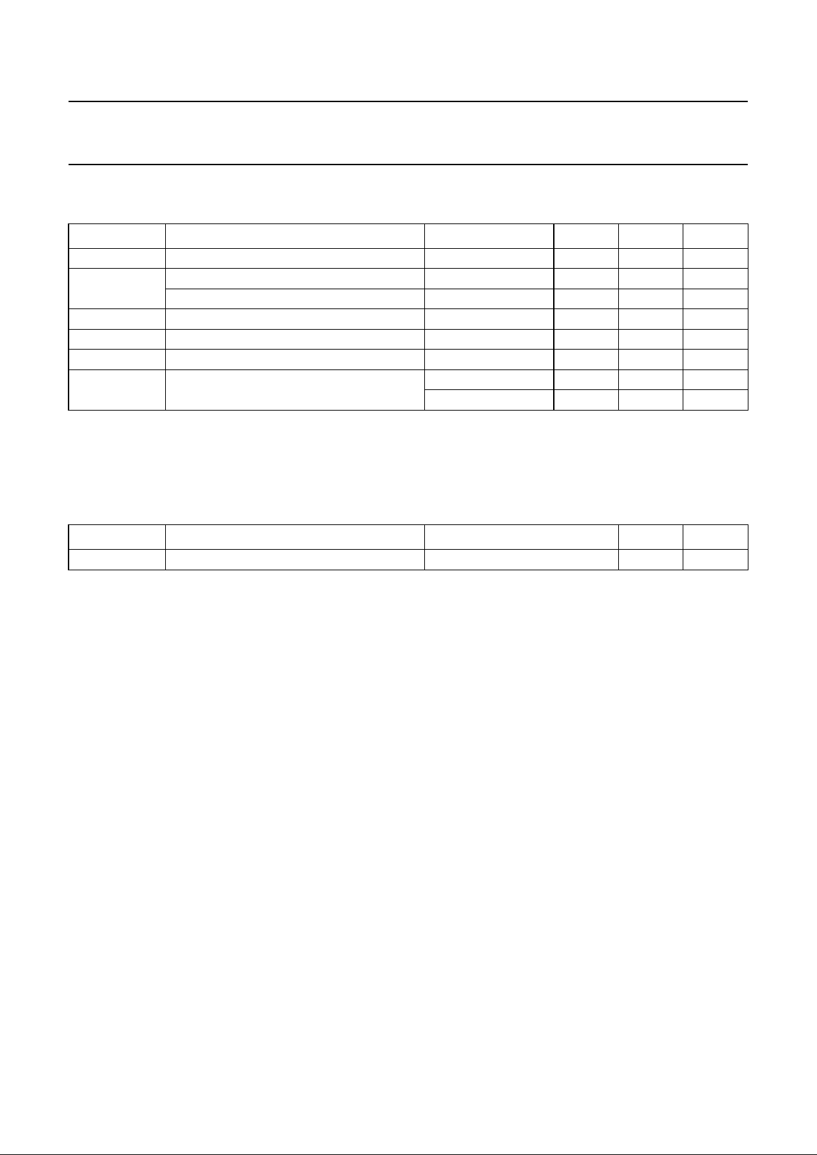
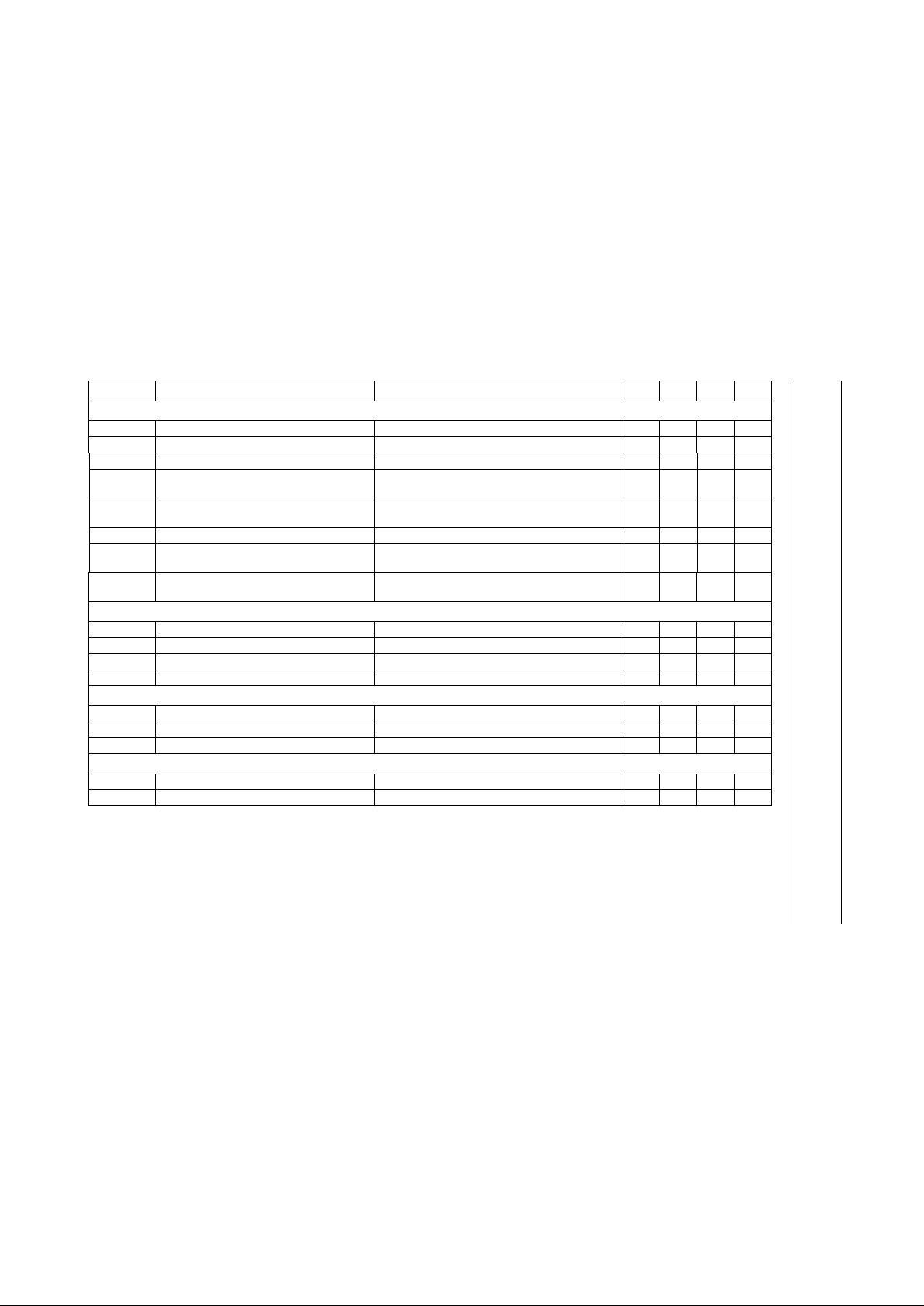
4 QUICK REFERENCE DATA
SYMBOL PARAMETER CONDITIONS MIN. TYP. MAX. UNIT
V
CC
supply voltage 7.8 8.5 9.2 V
I
CC
supply current 32 40 48 mA
Stereo decoder path
S/N signal-to-noise ratio − 78 − dB
THD total harmonic distortion − 0.1 − %
α
cs
channel separation 40 −−dB
V
o(rms)
output voltagelevelatpinsROPOand
LOPO
FM: 91% modulation;
AM: 100% modulation;
f
mod
= 400 Hz
840 950 1060 mV
Tone volume control
V
o(rms)
maximum output voltage level at pins
LF, LR, RF and RR
VCC= 8.5 V; THD ≤ 0.1% 2000 −−mV
G
v
voltage gain 1 dB steps −112 − +20 dB
G
step(vol)
step resolution (volume) − 1 − dB
G
bass
bass control −18 − +18 dB
G
treble
treble control −14 − +14 dB
G
step(treble, bass)
step resolution (bass and treble) − 2 − dB
(S + N)/N signal-plus-noise to noise ratio V
o
= 2.0 V; Gv= 0 dB;
unweighted
− 107 − dB
THD total harmonic distortion V
o(rms)
= 1.0 V; Gv=0dB − 0.01 − %
RR
100
ripple rejection V
r(rms)
< 200 mV;
f = 100 Hz; Gv=0dB
− 70 − dB
CMRR common mode rejection ratio
differential stereo input
48 53 − dB
2000 May 08 5
Philips Semiconductors Product specification
Up-level Car radio Analog Signal
Processor (CASP)
TEA6880H
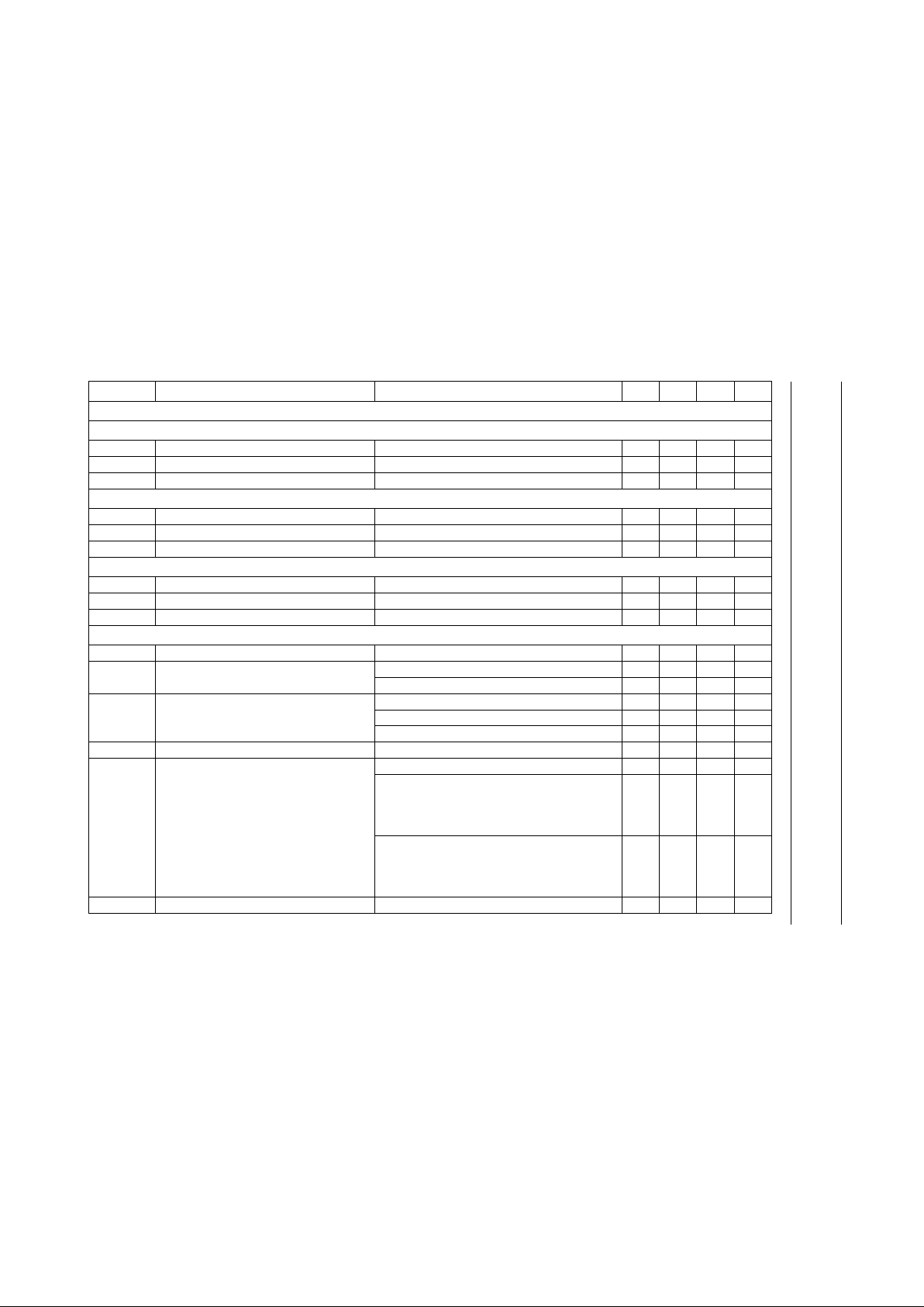
5 BLOCK DIAGRAM
Fig.1 Block diagram (continued in Fig.2).
MHB427
handbook, full pagewidth
50/75 µs
DE-EMPHASIS
&
AM STEREO INPUT
FM BUFFER
&
FM NB-GATES
MATRIX
&
SOFT-MUTE
V/I
CONVERTER
STEREO
DECODER
PLL
INPUT BUFFER
&
80 kHz
LOW-PASS
STEREO
DECODER
OUTPUT
AVERAGE
DETECTOR
(USN1)
AVERAGE
DETECTOR
(WBAM1)
PEAK
DETECTOR
(USN2)
AVERAGE
DETECTOR
(MUTE/HCC)
AM
GATE
LEVEL
ADC
(6-BIT)
LEVEL
INPUT
BUFFER
20 kHz
BAND-PASS
&
AMWB
DETECTOR
HCC
SNC
de-emphasis
switch
I2C-BUS
&
CONTROL LOGIC
I
2
C-bus
to NICE
from AM/FM
level detector
I
2
C-bus
detector hold
detector reset
test
NOISE
&
INTERFERENCE
DETECTOR
FM
PULSE
FORMER
sensitivity
start/
slope
BUS
start/
slope
38 kHz
19 kHz
38 kHz
mute slope
mute start
bus controls
22 kΩ
82 kΩ100 kΩ
22 kΩ
5
4
3
21
64
63
6 7
V
DD(I
2
C-bus)
4.7 nF
10 nF
4.7 nF
62
61
2.7 nF
2.7 nF
60
59
3.3 nF
58
57
53
52
51 50 49 48 47
46
45
44
43
54
55
10 nF
220 nF
56
10 µF
10 nF
3.3 nF
220 nF
33 pF
H
G
E
PEAK
DETECTOR
(WBAM2)
PEAK
DETECTOR
(SNC)
D
C
F
detector
hold
detector
hold
B
A
detector
reset
test
sep.adj.
60 kHz
HIGH-PASS
&
USN
DETECTOR
PULSE
SEPARATOR
120 kHz
HIGH-PASS
AMPLIFIER
sensitivity
pilot
ind.
MPX
input
AMNBIN
MPXRDS
RIN 182 kΩ
470 kΩ
100 nF
6.8 nF
100
nF
22
nF
6.8 nF
68 kΩ
10 nF
100 nF
100
kΩ
220 kΩ
33 nF
AM
mono
input
audio
processing hold
(for RDS update)
from
NICE
(AFSAMPLE)
f
ref
(75.4 kHz)
trigger sensitivity
TEA6880H
AGC
2000 May 08 6
Philips Semiconductors Product specification
Up-level Car radio Analog Signal
Processor (CASP)
TEA6880H
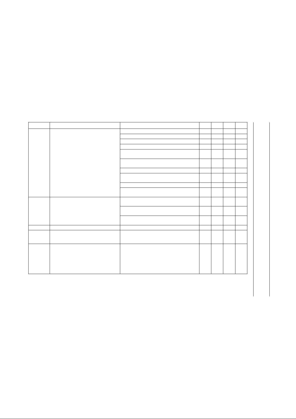
Fig.2 Block diagram (continued from Fig.1).
MHB428
handbook, full pagewidth
INTERNAL
POWER
SUPPLY
PEAK
TO
AVERAGE
DETECTOR
AM
PULSE
FORMER
SOURCE SELECTOR
&
REAR SEAT AUDIO SELECTOR
USN
ADC
(3-BIT)
BUS
BUS
address
select
input
diagnostic
&
chime
B
left
C
right
15 17
9
10
V
CC
(+8.5 V)
8
100 nF
C
ELFI
22 µF
18 19
1 µF
C
common
1 µF
16
220
nF
B
right
1412
11
13
220nF
AUDIO
BLEND CONTROL
(ABC)
ANALOG STEP
INTERPOLATION
(ASI)
31
30
32
42 41
40
39 38
E
WBAM
ADC
(3-BIT)
BUS
D
LOUDNESS
LEFT
C
H
G
F
B
A
CHIME ADDER
(G = −20 dB)
&
SWITCH
330
pF
35 34
15 nF
10
nF
220
nF
220
nF
3.3
kΩ
220 nF
220 nF
3.3 kΩ
29
28
27
26
25
68 nF
680 nF
C
KVR
220 nF
4.7 kΩ
43 kΩ
68
nF
680 pF
220 nF
C
KVL
4.7 kΩ
43 kΩ
10 nF
100 nF
24
23
22
47 µF
1 µF
220 nF
C
KIL
C
VHS
220 nF
C
KIR
A left
100 nF
21
20
100 nF
A right
C left
AM noise
blanker flag
37
left front
output
36
left rear
output
TEA6880H
BUS
BUS
BUS
BUS
BUS
BUS
CHIME ADDER
(G = −20 dB)
&
SWITCH
33
right front
output
BUS
VOLUME 1
LEFT
LEFT
TREBLE
BAND
LEFT
BASS
BAND
VOLUME 2
LEFT
FRONT
REAR
SEAT
AUDIO
SWITCH
VOLUME 2
LEFT
REAR
VOLUME 2
RIGHT
REAR
ASI/ABC
control
ASI
ABC
LOUDNESS
RIGHT
BUS
BUS
BUS
BUS
VOLUME 1
RIGHT
RIGHT
TREBLE
BAND
RIGHT
BASS
BAND
ASI
ABC
BUS
right rear
output
BUS
BUS
VOLUME 2
RIGHT
FRONT
BUS
D input
mono
symmetric

2000 May 08 7
Philips Semiconductors Product specification
Up-level Car radio Analog Signal
Processor (CASP)
TEA6880H
6 PINNING
SYMBOL PIN DESCRIPTION
SDAQ 1 data output (to TEA6840H)
SCLQ 2 clock output (to TEA6840H)
LEVEL 3 FM and AM level input (from TEA6840H)
SCL 4 I
2
C-bus clock
SDA 5 I
2
C-bus data
DGND 6 digital ground
TBL 7 time constant for FM modulation detector
V
CC
8 supply voltage
CHIME 9 chime tone input
AGND 10 analog ground
LLN 11 loudness left network
LOPI 12 left option port input (terminal impedance typical 100 kΩ)
LOPO 13 left option port output
BRI 14 channel B right stereo input (terminal impedance typical 100 kΩ)
ADR 15 address select
BLI 16 channel B left stereo input (terminal impedance typical 100 kΩ)
SCAP 17 supply filter capacitor
CRIP 18 channel C right symmetrical input (terminal impedance typical 30 kΩ)
CCOM 19 channel C common input (terminal impedance typical 30 kΩ)
CLIP 20 channel C left symmetrical input (terminal impedance typical 30 kΩ)
MONOC 21 mono common input (terminal impedance typical 30 kΩ)
MONOP 22 mono symmetrical input (terminal impedance typical 30 kΩ)
VHS 23 half supply filter capacitor
ARI 24 channel A right stereo input (terminal impedance typical 100 kΩ)
AMNCAP 25 peak-to-average detector capacitor for AM noise blanker
ALI 26 channel A left stereo input (terminal impedance typical 100 kΩ)
ROPO 27 right option port output
ROPI 28 right option port input (terminal impedance typical 100 kΩ)
RLN 29 loudness right network
RTC 30 right treble capacitor
RBI 31 right bass network input
RBO 32 right bass network output
RF 33 right front output
RR 34 right rear output
ASICAP 35 analog step interpolate capacitor
LR 36 left rear output
LF 37 left front output
LBO 38 left bass network output
LBI 39 left bass network input
LTC 40 left treble capacitor

2000 May 08 8
Philips Semiconductors Product specification
Up-level Car radio Analog Signal
Processor (CASP)
TEA6880H
AMPCAP 41 AM blanking time capacitor
AMHOLD 42 AM noise blanker flag
AMHCAP 43 AM noise blanker hold capacitor
I
ref
44 temperature independent reference current
TWBAM2 45 time constant for AM wideband peak detector
TUSN2 46 time constant for ultrasonic noise peak detector
PHASE 47 phase detector
f
ref
48 frequency reference input (75.4 kHz from TEA6840H)
PILOT 49 pilot on/off output
AFSAMPLE 50 reset for multipath detector (from TEA6840H for RDS update)
FMHOLD 51 FM audio processing hold input (from TEA6840H for RDS update)
AMHIN 52 AM signal input (from TEA6840H)
AMNBIN 53 AM noise blanker input (from TEA6840H)
TMUTE 54 time constant for soft mute
MPXRDS 55 unmuted MPX input (from TEA6840H for RDS update)
TSNC 56 time constant for stereo noise canceller
MPXIN 57 MPX input (from TEA6840H)
FMNCAP 58 FM noise detector capacitor
DEEML 59 left de-emphasis capacitor
DEEMR 60 right de-emphasis capacitor
FMLBUF 61 left AM/FM audio buffer capacitor
FMRBUF 62 right AM/FM audio buffer capacitor
TWBAM1 63 time constant for AM wideband average detector
TUSN1 64 time constant for ultrasonic noise average detector
SYMBOL PIN DESCRIPTION
2000 May 08 9
Philips Semiconductors Product specification
Up-level Car radio Analog Signal
Processor (CASP)
TEA6880H
handbook, full pagewidth
TEA6880H
MHB408
1
2
3
4
5
6
7
8
9
10
11
12
13
14
15
16
17
18
19
51
50
49
48
47
46
45
44
43
42
41
40
39
38
37
36
35
34
33
20
21
22
23
24
25
26
27
28
29
30
31
32
64
63
62
61
60
59
58
57
56
55
54
53
52
TUSN1
TWBAM1
FMRBUF
FMLBUF
DEEMR
DEEML
FMNCAP
MPXIN
TSNC
MPXRDS
TMUTE
AMNBIN
AMHIN
FMHOLD
AFSAMPLE
PILOT
SCAP
CRIP
CCOM
CLIP
MONOC
MONOP
VHS
ARI
AMNCAP
ALI
ROPO
ROPI
RLN
RTC
RBI
RBO
SDAQ
SCLQ
LEVEL
SCL
SDA
DGND
TBL
V
CC
CHIME
AGND
LLN
LOPI
LOPO
BRI
ADR
BLI
f
ref
PHASE
TUSN2
TWBAM2
I
ref
AMHCAP
AMHOLD
AMPCAP
LTC
LBI
LBO
LF
LR
ASICAP
RR
RF
Fig.3 Pin configuration.

2000 May 08 10
Philips Semiconductors Product specification
Up-level Car radio Analog Signal
Processor (CASP)
TEA6880H
7 FUNCTIONAL DESCRIPTION
7.1 Stereo decoder
The MPX input is the null-node of an operational amplifier
with internal feedback resistor. Adapting the stereo
decoder input to the level of the MPX signal, coming from
the FM demodulator output, is realized by the value of the
input series resistor RIN. To this input a second source
(AM detector output) can be fed by current addition.
The input amplifier is followed by an integrated 4th order
Bessel low-pass filter with a cut-off frequency of 80 kHz.
It provides necessary signal delay for FM noise blanking
and damping of high frequency interferences coming to
the stereo decoder input.
Output of this filter is fed to the soft mute control circuitry,
the output is voltage to current converted and then fed to
phase detector, pilot detector and pilot canceller circuits,
contained in the stereo decoder PLL block. For
regeneration of the 38 kHz subcarrier, a PLL is used.
The fully integrated oscillator is adjusted by means of a
digitalauxiliaryPLLintothecapture range of the main PLL.
The auxiliary PLL needs an external reference frequency
(75.4 kHz) which is provided by the TEA6840H.
The required 19 and 38 kHz signals are generated by
division of the oscillator output signal in a logical circuitry.
The 19 kHz quadrature phase signal is fed to the 19 kHz
phase detector, where it is compared with the incoming
pilot tone. The DC output signal of the phase detector
controls the oscillator (PLL).
The pilot presence detector is driven by an internally
generated in-phase 19 kHz signal. Its pilot dependent DC
output voltage is fed to a threshold switch, which activates
thepilotindicatorbitandturnsthestereodecoderto stereo
operation. The same DC voltage is used to control the
amplitude of an anti-phase internally generated 19 kHz
signal. In the pilot canceller, the pilot tone is compensated
by this anti-phase 19 kHz signal.
The pilot cancelled signal is fed to the matrix. There, the
side signal is demodulated and combined with the main
signal to left and right audio channel. Compensation for
roll-off in the incoming MPX signal caused by IF filters and
FM demodulator is typically realized by an external
compensation network at pin 57, individual alignment is
achieved by I2C-bus controlled amplification of the side
signal (DAA). A smooth mono to stereo takeover is
achieved by controlling the efficiency of the matrix with
help of the SNC peak detector.
The matrix is followed by the FM noise suppression gates,
which are combined with FM single poles and High Cut
Control (HCC). The single pole is defined by internal
resistors and external capacitors. From the gate circuits
audio is fed to the switchable de-emphasis, where the
demodulated AM stereo signal can be fed in. After
de-emphasis the signal passes to the output buffers and is
fed to the radio input of the source selector. For HCC, the
time constant of the single pole contained in the output
buffer can be changed to higher values. This function is
controlled by an average detector contained in the
multipath and fading detector.
7.2 FM noise blanker
The input of the ignition noise blanker is coupled to the
MPXRDS (pin 55) input signal and to the IF level input
(pin 3). Both signals are fed via separate 120 kHz filters
and rectifiers to an adder circuit. The output signal of the
adder circuit is fed in parallel to the noise detector and the
interference detector. The noise detector is a negative
peak detector. Its output controls the trigger sensitivity
(prevention to false triggering at noisy input signals) and
the gain of the MPX high-pass filter. The output of the
interferencedetector,whenreceivingasteeppulse,firesa
monoflop, contained in the pulse former circuitry. The time
constantofthemonoflopis defined by aninternalcapacitor
and its output activates the blanking gates in the audio.
7.3 AM noise blanker
The AM noise blanking pulse is derived from the AM audio
signal which is fed into pin 53 with the help of a
peak-to-averagecomparator. The blanking time is set by a
pulse former with external capacitor. The blanking pulse is
fed to the gate in the AM audio path and out to pin
AMHOLD to operate the gate built into the external
AM stereo processor.
7.4 Multipath/fading detection and weak signal
control
For FM signal quality dependent controls there is built-in a
combinationofsixdetectorsdrivenbythelevelinformation
direct, by the AC components on the level via a 20 kHz
band-pass filter (AM wideband) or the high notes present
at the FM demodulator output via a 60 kHz high-pass filter
(ultrasonic noise). The relation between DC level and the
AC components is programmable by the I2C-bus (2 bits
each). Output of level buffer, AM wideband detector and
ultrasonic noise detector are analog-to-digital converted
and readable by the I2C-bus.

2000 May 08 11
Philips Semiconductors Product specification
Up-level Car radio Analog Signal
Processor (CASP)
TEA6880H
For the time of fast RDS updating soft mute, SNC and
HCC can be put on hold and the AM wideband peak
detector and the ultrasonic noise peak detector are put on
reset by a switch signal delivered from the TEA6840H via
pin 51 (FMHOLD).
The six separate detecting circuits are:
1. The AM wideband noise peak detector is driven from
a 20 kHz band-pass filter connected to the level buffer
output. The time constant is defined by an external
capacitor at pin 45 (TWBAM2). The output voltage of
the detector is analog-to-digital converted by 3-bit.
2. The AM wideband noise average detector is driven
from a 20 kHz band-pass filter connected to the level
buffer output. The time constant is defined by an
external capacitor at pin 63 (TWBAM1). The output of
the detector is connected to the Stereo Noise Control
(SNC) circuit.
3. The ultrasonic noise peak detector is driven from a
60 kHz high-pass filter connected to the MPX signal
from pin 55 (MPXRDS). The time constant is defined
byanexternalcapacitorat pin 46 (TUSN2). Theoutput
voltage of the detector is analog-to-digital converted
by 3-bit.
4. The ultrasonic noise average detector is driven from a
60 kHz high-pass filter connected to the MPX signal
from pin 55 (MPXRDS). The time constant is defined
byanexternalcapacitorat pin 64 (TUSN1). Theoutput
of the detector is connected to soft mute control and
stereo noise control circuits.
5. For soft mute and high cut control purposes an
average detector with externally defined time constant
(TMUTE, pin 54) is provided. The detector is driven by
level output only. Soft mute as well as high cut control
can be switched off by the I2C-bus.
6. The stereo noise control peak detector with externally
defined time constant (TSNC, pin 56) is driven by
DC level output, AM wideband and ultrasonic noise
outputs. It provides the stereo blend facility (SNC).
Startingpoint and slope of stereo blend can be chosen
by the I2C-bus controlled reference voltage.
7.5 Tone/volume control
The tone/volume control part consists of the following
functions:
• Source selector
• Loudness
• Volume 1
• Treble
• Bass
• Volume 2
• Rear Seat Audio (RSA) selector
• Chime adder
• Analog step interpolation
• Audio blend control.
The stages loudness, volume 1, bass, and volume 2
include the Analog Step Interpolation (ASI) function. This
minimizes pops by smoothing out the transitions in the
audio signal during switching. The transition time is
I2C-bus programmable in a range of 1 : 24 in four steps.
The stages loudness, volume 1, and volume 2 also have
the Audio Blend Control (ABC) function. This minimizes
pops by automatically incrementing the volume and
loudnesscontrolsthrougheachstep between theirpresent
settings and the new settings. The speed of the ABC
function is correlated with the transition time of the ASI
function.
All stages are controlled via the I2C-bus.

2000 May 08 12
Philips Semiconductors Product specification
Up-level Car radio Analog Signal
Processor (CASP)
TEA6880H
7.5.1 SOURCE SELECTOR
The source selector allows the selection between
6 sources:
• 2 external stereo inputs (ALI, ARI, BLI and BRI)
• 1 external symmetrical stereo input (CLIP, CRIP and
CCOM)
• 1 external symmetrical mono input (MONOP and
MONON)
• 1 internal stereo input (AM/FM)
• 1 chime/diagnostic mono input (CHIME).
Via the chime/diagnostic mono input a chime input signal
can be sent to any audio output, at any volume level.
7.5.2 LOUDNESS
The output of the source selector is fed into the loudness
circuit via the external capacitors C
KVL
(pins LOPO and
LOPI) and C
KVR
(pins ROPO and ROPI). Depending on
the external circuits for the left and the right channel only a
bass boost or bass and treble boost is available. With the
external circuits shown in Figs 13 and 15 the curves from
Figs 14 and 16 will be obtained (without influence of C
KVL
respectively C
KVR
).
7.5.3 VOLUME 1
The volume 1 control follows behind the loudness circuit.
The control range of volume 1 is between +20 and −36 dB
in steps of 1 dB.
7.5.4 TREBLE
The output signal of the volume 1 control is fed into the
treble control stage. The control range is between
+14 and −14 dB in steps of 2 dB. Fig.20 shows the control
characteristic with external capacitors of 10 nF.
7.5.5 BASS
Thebasscontrolisthenext stage. The characteristic of the
bass curves depends upon the external circuits at
pins LBO/LBI (left channel) and RBO/RBI (right channel)
and also upon the setting of BSYM bit (MSB of the bass
control byte). With BSYM = 1, an equalizer characteristic
and with BSYM = 0, a shelving characteristic is obtained.
Figures 17 and 18 show the bass curves with an external
circuit of 2 × 220 nF and R = 3.3 kΩ for each channel with
different values for BSYM. Figure 19 shows the bass
curves with an external capacitor of 47 nF for each
channel and BSYM = 0, for boost and cut.
7.5.6 VOLUME 2
The four volume 2 blocks are located at the end of the
tone/volume control. In addition to volume control (same
settings as volume 2) also the balance and fader functions
are performed by individual attenuation offsets for the four
attenuators. The control range of these attenuators is
56 dB in steps of 1 dB and additional the steps −58.5 dB,
−62 dB, −68 dB, and a mute step.
7.5.7 RSA SELECTOR
The RSA selector provides the possibility to select an
alternative source for the rear channels. In this event rear
channels are only controlled by volume 2 function.
7.5.8 CHIME ADDER
With the chime adder circuit the chime input signal can be
summed with the left front and/or right front audio, or be
turned off.
2000 May 08 13
Philips Semiconductors Product specification
Up-level Car radio Analog Signal
Processor (CASP)
TEA6880H
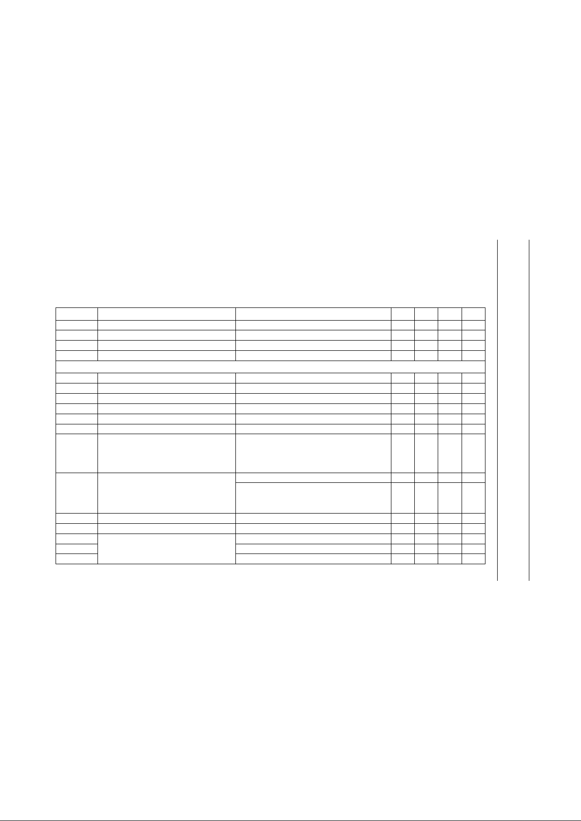
8 LIMITING VALUES
In accordance with the Absolute Maximum Rating System (IEC 60134).
Notes
1. Machine model (R = 0 Ω, C = 200 pF).
2. Human body model (R = 1.5 kΩ, C = 100 pF).
9 THERMAL CHARACTERISTICS
SYMBOL PARAMETER CONDITIONS MIN. MAX. UNIT
V
CC
supply voltage −0.3 +10 V
V
i
voltage at pins (except pins 4 and 5) VCC≤ 10 V VSS− 0.3 V
CC
V
voltage at pins 4 and 5 V
SS
− 0.3 9.7 V
P
tot
total power dissipation − 480 mW
T
stg
storage temperature −65 +150 °C
T
amb
operating ambient temperature −40 +85 °C
V
es
electrostatic handling for all pins note 1 −200 +200 V
note 2 −2000 +2000 V
SYMBOL PARAMETER CONDITIONS VALUE UNIT
R
th(j-a)
thermal resistance from junction to ambient in free air 48 K/W
2000 May 08 14
Philips Semiconductors Product specification
Up-level Car radio Analog Signal
Processor (CASP)
TEA6880H
10 CHARACTERISTICS
FM part: input signal V
i(MPX)(p-p)
= 1.89 V; m = 100% (∆f=±75 kHz, f
mod
= 400 Hz); de-emphasis of 75 µs and series resistor at input RIN= 182 kΩ;
FM audio measurements are taken at pins 13 and 27.
Tone part: R
S
= 600 Ω; RL=10kΩ, AC-coupled; CL= 2.5 nF; CLK = square-wave (5to 0 V) at 100 kHz; stereo source = A channel input; volume 1
attenuator = 0 dB; loudness=0dB, off; volume 2 attenuators = 0 dB; bass linear; treble linear; input voltage = 1 V, f = 1 kHz. Tone part audio
measurements are taken at pins 33 and 37. V
CC
= 8.3 to 8.7 V; VSS= 0; T
amb
=25°C; unless otherwise specified.
This IC shall not radiate noise in the audio system such that it disturbs any other circuit. This IC shall also not be susceptible to the radiation of any
other circuit.
SYMBOL PARAMETER CONDITIONS MIN. TYP. MAX. UNIT
V
CC
supply voltage 7.8 8.5 9.2 V
I
CC
supply current VCC=8.5V 324048mA
V
HS
half supply voltage VCC= 8.5 V 3.75 4.25 4.75 V
I
ref
reference current VCC= 8.5 V; R
ext
= 100 kΩ 35 37 39 µA
FM signal path
V
i(MPX)(p-p)
MPX input signal (peak-to-peak value) Ri= 182 kΩ−1.89 − V
∆V
i(MPX)
overdrive margin of MPX input signal THD = 1% 6 −−dB
I
i
AF input current − 3.66 −µA
I
i(max)
maximum AF input current THD = 1% 7.32 −−µA
V
o(rms)
AF mono output signal (RMS value) 91% modulation without pilot 890 1000 1110 mV
∆V
out
AF mono channel balance without pilot; V13/V
27
−1 − +1 dB
α
cs
channel separation aligned setting of data byte 1, bit 0 to bit 3;
m = 30% modulation plus 9% pilot
L=1; R=0 404770dB
L=0; R=1 404770dB
THD total harmonic distortion V
i(MPX)(p-p)
= 1.89 V; f
mod
= 1 kHz without pilot − 0.1 0.3 %
V
i(MPX)(p-p)
= 1.89 V; f
mod
= 5 kHz
L=1; R=0 − 0.1 0.3 %
L=0; R=1 − 0.1 0.3 %
S/N signal-to-noise ratio f = 20 Hz to 15 kHz 75 78 − dB
α
19
pilot signal suppression f = 19 kHz 40 50 − dB
α
38
subcarrier suppression f= 38 kHz 35 50 − dB
α
57
f = 57 kHz 40 −−dB
α
76
f = 76 kHz 50 60 − dB
2000 May 08 15
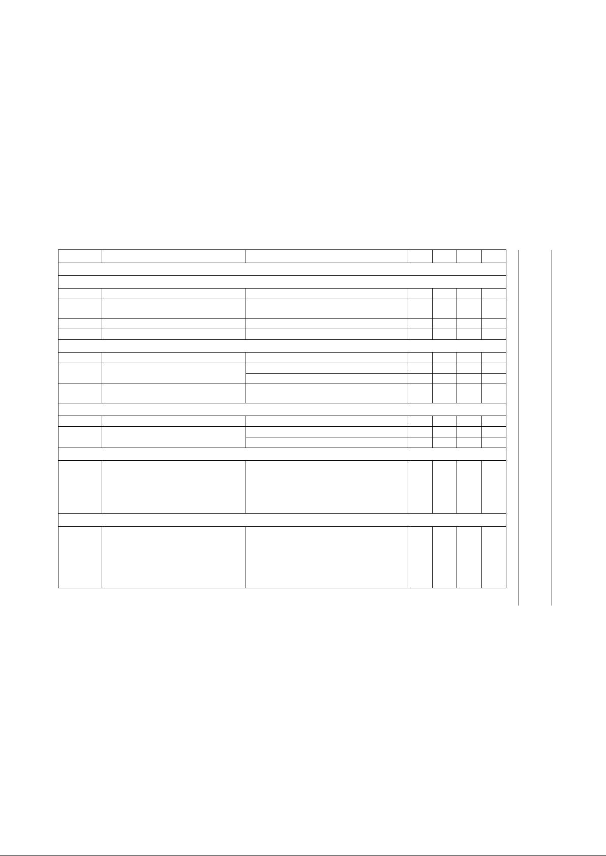
Philips Semiconductors Product specification
Up-level Car radio Analog Signal
Processor (CASP)
TEA6880H
IM2 second order intermodulation for f
spur
= 1 kHz f
mod
= 10 kHz; note 1 − 60 − dB
IM3 third order intermodulation for f
spur
= 1 kHz f
mod
= 13 kHz; note 1 − 58 − dB
α
57(RDS)
traffic radio (RDS) f = 57 kHz; note 2 − 70 − dB
α
67
Subsidiary Communication Authorization
(SCA)
f = 67 kHz; note 3 70 −−dB
α
114
Adjacent Channel Interference (ACI) f = 114 kHz; note 4 − 80 − dB
α
190
f = 190 kHz; note 4 − 70 − dB
PSRR power supply ripple rejection f = 100 Hz; V
ripple(rms)
= 100 mV − 30 − dB
R
S59
; R
S60
de-emphasis output source resistance data byte 3, bit 5 = 1; 75 µs 20 22.7 25.4 kΩ
data byte 3, bit 5 = 0; 50 µs 13.4 15.2 17 kΩ
I61; I
62
current capacity of FM buffer V
61,62
= 5.5 ±1V 50 − 200 µA
PLL VCO
f
osc
oscillator frequency − 228 − kHz
frequency range of free running oscillator 190 − 270 kHz
f
ref
reference frequency − 75.4 − kHz
V
i(fref)
reference frequency input voltage 30 100 500 mV
Z
i(48)
input impedance 100 −−kΩ
PLL pilot detector
V
i(pilot)(rms)
pilot threshold voltage for automatic switching
by pilot input voltage (RMS value)
stereo on; STIN = 1 − 27 37 mV
stereo off; STIN = 0 9 22 − mV
hys
(pilot)
hysteresis of pilot threshold voltage − 2 − dB
V
49-10
switching voltage for external mono control
(pin 49)
0.3 − 0.7 V
AM signal path
V
LOPO
;
V
ROPO
AC output voltage at pins 13 and 27 AMON= 1 and AMST = 0; Ri= 220 kΩ;
V
iAM(mono)
= 250 mV
195 245 295 mV
G
v
AM stereo audio buffer voltage gain subaddress0H: AMON = 1 and AMST = 1;
input signal at pin 59 or 60; coupled with 220 nF;
V
i(59,60)
= 200 mV; fi= 1 kHz; note 5
789dB
R
i(59,60)
input resistance for AM stereo left and right AMON = 1 and AMST = 1; note 6 80 100 120 kΩ
SYMBOL PARAMETER CONDITIONS MIN. TYP. MAX. UNIT
2000 May 08 16
Philips Semiconductors Product specification
Up-level Car radio Analog Signal
Processor (CASP)
TEA6880H
Noise blanker
FM PART
t
sup
interference suppression time 20 30 40 µs
I
offset
gate input offset current at pins during
suppression pulse duration
during AF suppression time − 20 50 nA
I
ch(FMNCAP)
charge current (into 4 V) −16 −12.5 −9.5 µA
I
dch(FMNCAP)
discharge current (from 5.5 V) 45 70 100 µA
Trigger Threshold Control (TTC), dependency on MPX signal at MPXRDS input
V
58-10
trigger threshold variation voltage V
i(MPXRDS)
= 0 V 4.5 5 5.5 V
∆V
58-10
trigger threshold voltage V
i(MPXRDS)
= 10 mV; f = 120 kHz 15 40 60 mV
V
i(MPXRDS)
= 100 mV; f = 120 kHz 75 100 200 mV
∆V
7-10
trigger threshold variation with audio
frequency f = 15 kHz
V
i(MPXRDS)
= 670 mV − 500 − mV
Trigger Threshold Control (TTC), dependency on level detector input signal
V
58-10
trigger threshold voltage V
LEVEL(AC)
= 0 V 4.5 5 5.5 V
∆V
58-10
trigger threshold voltage as a function of
V
LEVEL(AC)
V
LEVEL(AC)
= 10 mV; f = 120 kHz − 0 − mV
V
LEVEL(AC)
= 200 mV; f = 120 kHz − 40 − mV
Trigger sensitivity measurement with pulse (on MPX signal) at MPXRDS input
V
pulse
trigger sensitivity t
pulse
=10µs; write mode; data byte 3, bits 6 and 7:
NBS1 = 1; NBS0 = 1 − 60 − mV
NBS1 = 1; NBS0 = 0 − 100 − mV
NBS1 = 0; NBS0 = 1 − 150 − mV
NBS1 = 0; NBS0 = 0 − 200 − mV
Trigger sensitivity measurement with pulse (on level signal) at AM/FM level input
V
pulse
trigger sensitivity t
pulse
=10µs; V
3-10
= 0.5 V; write mode;
data byte 3, bits 6 and 7:
NBS1 = 1; NBS0 = 1 − 250 − mV
NBS1 = 1; NBS0 = 0 − 275 − mV
NBS1 = 0; NBS0 = 1 − 300 − mV
NBS1 = 0; NBS0 = 0 − 320 − mV
SYMBOL PARAMETER CONDITIONS MIN. TYP. MAX. UNIT
2000 May 08 17
Philips Semiconductors Product specification
Up-level Car radio Analog Signal
Processor (CASP)
TEA6880H
AM PART
m
mod
trigger threshold − 140 − %
t
h
hold time (suppression time) 400 500 600 µs
V
AMPCAP(AC)
AF voltage at pin 43 V
iAM(mono)
= 50 mV (RMS); f=1kHz 16 22 30 mV
α
AMGATE
attenuation of blanking gate V
iAM(mono)
= 50 mV (RMS); gate open: internal
voltage; gate closed: V
DC42-10
= 4 V; note 7
−60 −70 −80 dB
t
sup(AMHOLD)
suppression time at pin 42 t
pulse
=10µs; repetition rate = 50 Hz; V
pulse
= 1.7 V
(pin 53); V
3-10
= 0.5 V
400 500 600 µs
V
(25-10)DC
detector voltage; V
ext(53-10)DC
− 0.7 V V
53(AC)
=0V; V
(3-10)DC
= 3.5 V 3.3 3.8 4.3 V
f
42
trigger sensitivity t
pulse
=10µs; repetition rate = 50 Hz; V
pulse
= 1.7 V
(pin 53); V
3-10
=4V
45 50 55 Hz
I
offset
gate input offset current at pins during
suppression pulse duration
during AF suppression time −50 0 +50 nA
Muting average detector (pin 54); see Fig.12
V
i(LEVEL)
input voltage on pin LEVEL 0.5 − 4V
G
v
voltage gain pin 3 to pin 54 − 0 − dB
∆V
TMUTE
offset between pins 3 and 54 − 1.5 − V
∆V
TMUTE/K
temperature dependence at pin 54 − 3.3 − mV/K
MUTING AVERAGE DETECTOR TIME CONSTANT
I
ch(TMUTE)
TMUTE charge current − 0.2 −µA
I
dch(TMUTE)
TMUTE discharge current −−0.2 −µA
V
O
DC output voltage 2 − 5V
TEST CONDITION
I
ch(test)
capacitor charge current data byte6, bit7=1 − 12 −µA
I
dch(test)
capacitor discharge current data byte 6, bit7=1 −−12 −µA
SYMBOL PARAMETER CONDITIONS MIN. TYP. MAX. UNIT

2000 May 08 18
Philips Semiconductors Product specification
Up-level Car radio Analog Signal
Processor (CASP)
TEA6880H
AM wideband average detector (pin 63); see Fig.6
V
TWBAM1
DC voltage at TWBAM1 w.r.t pin 10 V
LEVEL(AC)
= 400 mV;V
LEVEL(DC)
= 3.5 V;fi= 24 kHz;
write mode; data byte 1, bits 4 and 5:
AWS1 = 1; AWS0 = 1 − 4.10 − V
AWS1 = 1; AWS0 = 0 − 3.60 − V
AWS1 = 0; AWS0 = 1 − 3.00 − V
AWS1 = 0; AWS0 = 0 − 2.35 − V
VC
TWBAM1
DC voltage coefficient V
LEVEL(AC)
= 400 mV;V
LEVEL(DC)
= 3.5 V;fi= 24 kHz;
write mode; note 8; data byte 1, bits 4 and 5:
AWS1 = 1; AWS0 = 1 0.69 0.82 0.98
AWS1 = 1; AWS0 = 0 0.60 0.72 0.86
AWS1 = 0; AWS0 = 1 0.50 0.60 0.71
AWS1 = 0; AWS0 = 0 0.40 0.47 0.56
V
O
DC output voltage 1.5 − 5.5 V
AM WIDEBAND AVERAGE DETECTOR TIME CONSTANT
I
ch(TWBAM1)
TWBAM1 charge current 11.5 15 19.5 µA
I
dch(TWBAM1)
TWBAM1 discharge current −19.5 −15 −11.5 µA
Ultrasonic noise average detector (pin 64); see Fig.5
V
TUSN1
DC voltage at TUSN1 w.r.t. pin 10 V
MPXRDS(AC)
= 350 mV; V
LEVEL(DC)
= 3.5 V;
fi= 80 kHz; write mode; data byte 1, bits 6 and 7:
USS1 = 1; USS0 = 1 − 4.25 − V
USS1 = 1; USS0 = 0 − 4.00 − V
USS1 = 0; USS0 = 1 − 3.50 − V
USS1 = 0; USS0 = 0 − 2.60 − V
VC
TUSN1
DC voltage coefficient V
MPXRDS(AC)
= 350 mV; V
LEVEL(DC)
= 3.5 V;
fi= 80 kHz; write mode; note 9; data byte 1,
bits 6 and 7:
USS1 = 1; USS0 = 1 0.71 0.85 1.00
USS1 = 1; USS0 = 0 0.67 0.80 0.95
USS1 = 0; USS0 = 1 0.60 0.70 0.85
USS1 = 0; USS0 = 0 0.44 0.52 0.62
V
O
DC output voltage 1.5 − 5.5 V
SYMBOL PARAMETER CONDITIONS MIN. TYP. MAX. UNIT

2000 May 08 19
Philips Semiconductors Product specification
Up-level Car radio Analog Signal
Processor (CASP)
TEA6880H
ULTRASONIC NOISE AVERAGE DETECTOR TIME CONSTANT
I
ch(TUSN1)
TUSN1 charge current 11.5 15 19.5 µA
I
dch(TUSN1)
TUSN1 discharge current −19.5 −15 −11.5 µA
Peak detector for stereo noise control (SNC, pin 56)
DEPENDENCY ON LEVEL VOLTAGE; see Fig.12
V
LEVEL
input voltage 0.5 − 4.75 V
G gain pin 3 to pin 56 − 0 − dB
V
TSNC
DC voltage at TSNC referred to DC level
voltage at pin 3
without MPXRDS and LEVEL (AC) input
V
(3-10)DC
= 0.5 V 1.75 2.00 2.25 V
V
(3-10)DC
= 3.5 V 4.50 5.00 5.50 V
∆V
TSNC/K
temperature dependence at pin 56 − 3.3 − mV/K
DEPENDENCY ON ULTRASONIC NOISE; see Fig.5
V
TSNC
DC voltage at TSNC w.r.t. pin 10 V
MPXRDS(AC)
= 350 mV; V
(3-10)DC
= 3.5 V;
fi= 80 kHz; write mode; data byte 1, bits 6 and 7:
USS1 = 1; USS0 = 1 − 4.25 − V
USS1 = 1; USS0 = 0 − 4.00 − V
USS1 = 0; USS0 = 1 − 3.50 − V
USS1 = 0; USS0 = 0 − 2.60 − V
VC
TSNC
DC voltage coefficient V
MPXRDS(AC)
= 350 mV; V
(3-10)DC
= 3.5 V;
fi= 80 kHz; write mode; note 10; data byte 1,
bits 6 and 7:
USS1 = 1; USS0 = 1 0.71 0.85 1.00
USS1 = 1; USS0 = 0 0.67 0.80 0.95
USS1 = 0; USS0 = 1 0.60 0.70 0.85
USS1 = 0; USS0 = 0 0.44 0.52 0.62
V
O
DC output voltage 2 − 5V
SYMBOL PARAMETER CONDITIONS MIN. TYP. MAX. UNIT

2000 May 08 20
Philips Semiconductors Product specification
Up-level Car radio Analog Signal
Processor (CASP)
TEA6880H
DEPENDENCY ON AM WIDEBAND NOISE; see Fig.6
V
TSNC
DC voltage at TSNC V
LEVEL(AC)
= 400 mV;V
LEVEL(DC)
= 3.5 V;fi= 24 kHz;
write mode; data byte 1, bits 4 and 5:
AWS1 = 1; AWS0 = 1 − 4.10 − V
AWS1 = 1; AWS0 = 0 − 3.60 − V
AWS1 = 0; AWS0 = 1 − 3.00 − V
AWS1 = 0; AWS0 = 0 − 2.35 − V
VC
TSNC
DC voltage coefficient V
LEVEL(AC)
= 400 mV;V
LEVEL(DC)
= 3.5 V;fi= 24 kHz;
write mode; note 11; data byte 1, bits 4 and 5:
AWS1 = 1; AWS0 = 1 0.69 0.82 0.98
AWS1 = 1; AWS0 = 0 0.60 0.72 0.86
AWS1 = 0; AWS0 = 1 0.50 0.60 0.71
AWS1 = 0; AWS0 = 0 0.40 0.47 0.56
V
O
DC output voltage 1.5 − 5.5 V
DETECTOR TIME CONSTANT
I
ch(TSNC)
TSNC charge current −−2.3 −µA
I
dch(TSNC)
TSNC discharge current − 65 −µA
TEST CONDITION
I
ch(test)
charge current for testing data byte 6, bit 7 = 1; V
(3-10)DC
=2V;
V
(56-10)DC
= 2.8 V
−−1.5 − mA
I
dch(test)
discharge current for testing data byte 6, bit 7 = 1; V
(3-10)DC
=2V;
V
(56-10)DC
= 4.2 V
− 200 −µA
SYMBOL PARAMETER CONDITIONS MIN. TYP. MAX. UNIT

2000 May 08 21
Philips Semiconductors Product specification
Up-level Car radio Analog Signal
Processor (CASP)
TEA6880H
Ultrasonic noise peak detector (pin 46); see Fig.5
V
TUSN2
DC voltage at TUSN2 w.r.t. pin 10 V
MPXRDS(AC)
= 350 mV; V
(3-10)DC
= 3.5 V;
fi= 80 kHz; write mode; data byte 1, bits 6 and 7:
USS1 = 1; USS0 = 1 − 4.25 − V
USS1 = 1; USS0 = 0 − 4.00 − V
USS1 = 0; USS0 = 1 − 3.50 − V
USS1 = 0; USS0 = 0 − 2.60 − V
VC
TUSN2
DC voltage coefficient V
MPXRDS(AC)
= 350 mV; V
(3-10)DC
= 3.5 V;
fi= 80 kHz; write mode; note 12; data byte 1,
bits 6 and 7:
USS1 = 1; USS0 = 1 0.71 0.85 1.00
USS1 = 1; USS0 = 0 0.67 0.80 0.95
USS1 = 0; USS0 = 1 0.60 0.70 0.85
USS1 = 0; USS0 = 0 0.44 0.52 0.62
V
O
DC output voltage 1.5 − 5.5 V
DETECTOR TIME CONSTANT
I
ch(TUSN2)
TUSN2 charge current −−1.6 −µA
I
dch(TUSN2)
TUSN2 discharge current − 21 −µA
AM wideband peak detector (pin 45); see Fig.6
V
TWBAM2
DC voltage at TWBAM2 w.r.t pin 10 V
LEVEL(AC)
= 400 mV;V
LEVEL(DC)
= 3.5 V;fi= 24 kHz;
write mode; data byte 1, bits 4 and 5:
AWS1 = 1; AWS0 = 1 − 4.10 − V
AWS1 = 1; AWS0 = 0 − 3.60 − V
AWS1 = 0; AWS0 = 1 − 3.00 − V
AWS1 = 0; AWS0 = 0 − 2.35 − V
VC
TWBAM2
DC voltage coefficient V
LEVEL(AC)
= 400 mV;V
LEVEL(DC)
= 3.5 V;fi= 24 kHz;
write mode; note 13; data byte 1, bits 4 and 5:
AWS1 = 1; AWS0 = 1 0.69 0.82 0.98
AWS1 = 1; AWS0 = 0 0.60 0.72 0.86
AWS1 = 0; AWS0 = 1 0.50 0.60 0.71
AWS1 = 0; AWS0 = 0 0.40 0.47 0.56
V
O
DC output voltage 2 − 5V
SYMBOL PARAMETER CONDITIONS MIN. TYP. MAX. UNIT

2000 May 08 22
Philips Semiconductors Product specification
Up-level Car radio Analog Signal
Processor (CASP)
TEA6880H
DETECTOR TIME CONSTANT
I
ch(TWBAM2
) TWBAM2 charge current −−1.6 −µA
I
dch(TWBAM2)
TWBAM2 discharge current − 21 −µA
Soft mute; see Figs 7 and 4
α
0dB
attenuation at pins 13 and 27 V
TMUTE
= 3.5 V; V
TUSN1
= 3.5 V −0.5 0 +0.5 dB
α
6dB
start of muting; AC attenuation at
pins 13 and 27
see Fig.4; write mode; data byte 0, bits 0 and 1;
MSL0 = 1; MSL1 = 1
MST1 = 0; MST0 = 0; V
TMUTE
= 0.42V
TUSN1
without AC
369dB
MST1 = 0; MST0 = 1; V
TMUTE
= 0.45V
TUSN1
without AC
369dB
MST1 = 1; MST0 = 0; V
TMUTE
= 0.47V
TUSN1
without AC
369dB
MST1 = 1; MST0 = 1; V
TMUTE
= 0.49V
TUSN1
without AC
369dB
α
10dB
AC attenuation for setting of mute slope at
pins 13 and 27
MST1 = 0; MST0 = 0; see Fig.7
MSL1 = 0; MSL0 = 0; V
TMUTE(DC)
= 0.35V
TUSN1
without AC
7 1013dB
MSL1 = 0; MSL0 = 1; V
TMUTE(DC)
= 0.38V
TUSN1
without AC
7 1013dB
MSL1 = 1; MSL0 = 0; V
TMUTE(DC)
= 0.39V
TUSN1
without AC
7 1013dB
MSL1 = 1; MSL0 = 1; V
TMUTE(DC)
= 0.395V
TUSN1
without AC
7 1013dB
SYMBOL PARAMETER CONDITIONS MIN. TYP. MAX. UNIT

2000 May 08 23
Philips Semiconductors Product specification
Up-level Car radio Analog Signal
Processor (CASP)
TEA6880H
Stereo Noise Control (SNC)
α
cs(start)
start of channel separation aligned at L= 1 and R = 0;
data byte 2: SST[3:0] = 1111; V
TSNC
or V
TUSN1
or
V
TWBAM1
= 0.63V
TUSN1
without AC; see note 14 and
Fig.9
4.5 6 7.5 dB
aligned at L = 1 and R = 0;
data byte 2: SST[3:0] = 1000; V
TSNC
or V
TUSN1
or
V
TWBAM1
= 0.70V
TUSN1
without AC; see note 14 and
Fig.9
4.5 6 7.5 dB
aligned at L = 1 and R = 0;
data byte 2: SST[3:0] = 0000; V
TSNC
or V
TUSN1
or
V
TWBAM1
= 0.74V
TUSN1
without AC; see note 14 and
Fig.9
4.5 6 7.5 dB
α
cs(slope)
slope of channel separation aligned at L = 1 and R = 0;
data byte 2: SST[3:0] = 1000; V
TSNC
= 0.72V
TUSN1
without AC; see note 15 and Fig.8; data byte2,
bits 4 and 5:
SSL1 = 0; SSL0 = 0 357dB
SSL1 = 0; SSL0 = 1 579dB
SSL1 = 1; SSL0 = 0 11 13 15 dB
SSL1 = 1; SSL0 = 1 (not defined)
SYMBOL PARAMETER CONDITIONS MIN. TYP. MAX. UNIT

2000 May 08 24
Philips Semiconductors Product specification
Up-level Car radio Analog Signal
Processor (CASP)
TEA6880H
High Cut Control (HCC)
α
HCC(start)
AC attenuation for start of HCC AF = 10 kHz; V
MPXIN
= 200 mV; HSL1 = 1;
HSL0 = 0; data byte 0 SMUT = 0 and MONO= 1;
write mode; see note 16 and Fig.10; data byte 3,
bits 2 and 3:
HST1 = 1; HST0 = 1; V
(3-10)DC
= 1.30 V 1.5 3 4.5 dB
HST1 = 1; HST0 = 0; V
(3-10)DC
= 1.45 V 1.5 3 4.5 dB
HST1 = 0; HST0 = 1; V
(3-10)DC
= 1.90 V 1.5 3 4.5 dB
HST1 = 0; HST0 = 0; V
(3-10)DC
= 2.10 V 1.5 3 4.5 dB
α
HCC(slope)
AC attenuation for slope of HCC AF = 10 kHz; V
MPXIN
= 200 mV;
C
61-10,C62-10
= 2.7 nF; HST1 = 1; HST0 = 1;
data byte 0 SMUT = 0 and MONO = 1; write mode;
see note 16 and Fig.11; data byte 3, bits 0 and1:
HSL1 = 1; HSL0 = 1 5.5 7.5 9.5 dB
HSL1 = 1; HSL0 = 0 468dB
HSL1 = 0; HSL0 = 1 246dB
HSL1 = 0; HSL0 = 0 135dB
α
HCC(max)
maximum HCC attenuation AF = 10 kHz; V
TMUTE
= 2 V; data byte0, SMUT = 0
and MONO = 1; data byte 3, bit1=bit0=1
C
61-10
, C
62-10
= 2.7 nF; data byte 3 bit 4 = 1 8 10 14.5 dB
C
61 -10
, C
62-10
= 680 pF; data byte 3 bit4=0 8 10 14.5 dB
SYMBOL PARAMETER CONDITIONS MIN. TYP. MAX. UNIT
2000 May 08 25
Philips Semiconductors Product specification
Up-level Car radio Analog Signal
Processor (CASP)
TEA6880H
Analog-to-digital converters
LEVEL ANALOG-TO-DIGITAL CONVERTER (6-BIT)
V
LEVEL(min)
lower limit of conversion range 600 720 840 mV
V
LEVEL(max)
upper limit of conversion range 3.2 3.4 3.6 V
∆V
LEVEL
bit resolution − 44 − mV
ULTRASONIC NOISE ANALOG-TO-DIGITAL CONVERTER (3-BIT)
V
TUSN(min)
lower limit of conversion range 1.9 2.1 2.4 V
V
TUSN(max)
upper limit of conversion range 3.8 4.1 4.5 V
∆V
TUSN
bit resolution 280 330 380 mV
AM WIDEBAND NOISE ANALOG-TO-DIGITAL CONVERTER (3-BIT)
V
TWBAM(min)
lower limit of conversion range 1.9 2.1 2.4 V
V
TWBAM(max)
upper limit of conversion range 3.8 4.1 4.5 V
∆V
TWBAM
bit resolution 280 330 380 mV
Tone/volume control
G
v(max)
maximum voltage gain RS≤ 10 Ω; RL≥ 10 MΩ 19 20 21 dB
G
v(signal)
signal voltage gain T
amb
=25°C −0.75 0 +0.75 dB
T
amb
= −40 to +85 °C −1 0 +1 dB
V
o(rms)
output voltage level THD ≤ 0.5% − 2000 − mV
THD = 1%; G
v
= 3 dB 2300 −−mV
R
L
=2kΩ; CL= 10 nF; THD = 1% 2000 −−mV
V
i(rms)
input sensitivity Vo= 500 mV; Gv=20dB − 50 − mV
f
ro
roll-off frequency high frequency (−1 dB) 20000 −−Hz
input A; C
KIL=CKIR
= 100 nF;
C
KVL=CKVR
= 220 nF
low frequency (−1 dB) − 35 45 Hz
low frequency (−3 dB) − 20 25 Hz
input C; C
KICL=CKICR
=1µF;
C
KVL=CKVR
= 220 nF
low frequency (−1 dB) − 18 23 Hz
low frequency (−3 dB) − 10 13 Hz
α
cs
channel separation Vi= 1 V; frequency range 250 Hz to 20 kHz 74 80 − dB
SYMBOL PARAMETER CONDITIONS MIN. TYP. MAX. UNIT

2000 May 08 26
Philips Semiconductors Product specification
Up-level Car radio Analog Signal
Processor (CASP)
TEA6880H
THD total harmonic distortion valid for input channel A, B or C; same for all 4
outputs refer to inputs
V
i(rms)
= 1 V; f = 1 kHz;
volume 1 attenuator: −6 dB; equalizer bands flat
− 0.05 0.1 %
V
i(rms)
= 2 V; f = 1 kHz; VCC= 8.3 V;
volume 1 attenuator: −13 dB; equalizer bands flat
− 0.1 0.3 %
V
i(rms)
= 2 V; f = 1 kHz; VCC= 8.5 V;
volume 1 attenuator: 0 dB; equalizer bands flat
− 0.05 0.1 %
V
i(rms)
= 1 V; f = 1 kHz; VCC= 8.3 V;
volume 1 attenuator: 0 dB; equalizer bands flat
− 0.01 0.1 %
V
i(rms)
= 2.3 V; f = 1 kHz; VCC=9V;
volume 1 attenuator: −13 dB; equalizer bands flat
− 0.13 0.3 %
V
i(rms)
= 1 V; f = 20 Hz to 20 kHz;
volume 1 attenuator: −6 dB; equalizer bands flat
− 0.05 0.2 %
V
i(rms)
= 2 V; f = 20 Hz to 20 kHz; VCC= 8.3 V;
volume 1 attenuator: −13 dB; equalizer bands flat
− 0.1 0.3 %
V
i(rms)
= 2.3 V; f = 20 Hz to 20 kHz; VCC=9V;
volume 1 attenuator: −13 dB; equalizer bands flat
− 0.1 0.3 %
V
i(rms)
= 0.5 V; f = 25 Hz; volume 1
attenuator: 0 dB; equalizer bass boost: +8 dB
− 0.1 0.2 %
V
i(rms)
= 0.5 V; f = 4 kHz; volume 1
attenuator: 0 dB; equalizer treble boost: +8 dB
− 0.15 0.3 %
chime adder total harmonic distortion V
i(rms)
= 0.5 V; f = 1 kHz; VCC= 8.5 V;
no input signal at input A
− 0.04 0.1 %
PSRR power supply ripple rejection C
23
=47µF;
C17=22µF
stereo source: A, B, C or mono;
VCC= 8.5 V + 0.2 V (RMS)
f = 20 to 100 Hz 35 46 − dB
f=1to20kHz 50 65 − dB
f = 1 kHz 50 75 − dB
t
turn-on
turn-on time from VCCapplied to 66%final DC
voltage at outputs
SCAP = 22 µF; VHS = 47 µF − 250 − ms
SCAP = 10 µF; VHS = 10 µF − 100 − ms
SYMBOL PARAMETER CONDITIONS MIN. TYP. MAX. UNIT
2000 May 08 27
Philips Semiconductors Product specification
Up-level Car radio Analog Signal
Processor (CASP)
TEA6880H
V
noise(rms)
noise voltage CCIR-ARM weighted
(RMS value) without input signal and shorted
AF inputs
volume 1 attenuator: +20 dB − 65 100 µV
volume 1 attenuator: +20 dB; symmetrical input − 100 140 µV
volume 1 attenuator: 0 dB − 10 14 µV
volume 1 attenuator: 0 dB; symmetrical input − 12.5 18 µV
volume 1 attenuator: 0 dB;
bass and treble boost: 6 dB
− 16 25 µV
volume 1 attenuator: 0 dB;
bass and treble boost: 6 dB; symmetrical input
− 22 32 µV
volume 1 attenuator: −9dB − 914µV
minimum volume; volume 1attenuator: −18 dB;
loudness: −20 dB; volume 2 attenuator: −22 dB
− 58µV
mute selected: data byte 8, AMUT = 1 − 3.5 5 µV
volume setting: −20 dB; volume 1 attenuator:
−10 dB; loudness: −10 dB; A-weighted
− 5.7 8 µV
CMRR input common mode rejection C channel input;V
i(rms)
=1V;f=20Hzto20kHzon
CLIP, CRIP and CCOM
48 53 − dB
C channel input; V
i(rms)
= 1 V; f = 1 kHz on CLIP,
CRIP and CCOM
48 53 − dB
C channelinput; V
i(rms)
=1V;f=20Hzto20kHzon
CLIP, CRIP and CCOM; volume attenuator: −15 dB
63 68 − dB
CMRR
mono
mono input common mode rejection source = mono input 40 45 − dB
α
ct
crosstalk between bus inputs and signal
outputs
clock frequency = 50 kHz;
repetition burst rate = 300 Hz; total initialization;
note 17
− 110 − dB
t
ABC
Audio Blend Control (ABC) step time C
ASICAP
= 22 nF; write mode; data byte 4,
bits 6 and 7:
ASI1 = 0; ASI0 = 0 − 0.83 − ms
ASI1 = 0; ASI0 = 1 − 3.33 − ms
ASI1 = 1; ASI0 = 0 − 8.33 − ms
ASI1 = 1; ASI0 = 1 − 20 − ms
SYMBOL PARAMETER CONDITIONS MIN. TYP. MAX. UNIT
 Loading...