

Page 1

TEA5880TS
Integrated FM stereo radio IC for host processor tuning in
handheld applications
Rev. 02 — 26 April 2004 Preliminary data sheet
1. General description
The TEA5880TS stereo FM radio IC dramatically reduces the printed-circuit board area
(only 100 mm2) needed to integrate FM radio functionality into portable devices. This
makes it invaluable for any application where space is at a premium.
Relying on a system host processor for radio tuning, the TEA5880TS is ideally suited for
powerful devices such as PDAs, notebooks, portable CD and MP3 players.
2. Features
■ No alignments necessary
■ Complete adjustment-free stereo decoder; no external crystal required
■ Fully integrated MPX VCO circuit
■ Fully integrated low IF selectivity and demodulation
■ The full integration level means no or few external components required
■ No external FM discriminator needed due to full integration
■ Built-in adjacent channel interference total reduction (no 114 kHz, no 190 kHz)
■ The leveloftheincomingsignalatwhichtheradiomust lock is software programmable
■ Due to new tuning concept, the tuning is independent of the channel spacing
■ Very high sensitivity due to integrated low noise RF input amplifier
■ RF Automatic Gain Control (AGC) circuit
■ Standby mode for power-down, no power switch circuitry required
■ 2.7 V minimum supply voltage
■ MPX output for RDS
■ 3-wire bus
■ In combination withthe host, fast, low power operation of preset mode, manual search,
automatic search and automatic store are possible
■ Host can be in Sleep mode after tuning; a minute retuning is recommended to
compensate for temperature and voltage fluctuations
■ Covers all Japanese, European and US bands.
Page 2

Philips Semiconductors
TEA5880TS
Integrated FM stereo radio IC for host processor tuning
3. Quick reference data
Table 1: Quick reference data
V
= V
CCA
Symbol Parameter Conditions Min Typ Max Unit
V
V
I
CCA
I
CCD
I
LED
f
FM(ant)
T
FM overall system parameters
V
SUP
IP3
IP3
S
S
S
S
IR image rejection f
V
V
(S+N)/N maximum signal plus
α
CCA
CCD
amb
i(RF)
in
out
−300
+300
−200
+200
AUDL
AUDR
cs
CCD
analog supply voltage 2.7 3.0 5.0 V
digital supply voltage 2.7 3.0 5.0 V
analog supply current operating - 17 22 mA
standby - 1 100 µA
digital supply current operating - 250 500 mA
standby - 1 100 µA
optional stereo LED - 1 2 mA
FM input frequency 76 - 108 MHz
ambient temperature V
RF sensitivity input
voltage
V
CCA
CCA
= V
= V
CC(VCO)
CC(VCO)
= V
= V
= 3 V −10 - +75 °C
CCD
= 5 V −40 - +85 °C
CCD
fRF = 76 MHz to 108 MHz; ∆f = 22.5 kHz;
f
= 1 kHz; (S+N)/N = 26 dB;
mod
-13µV
de-emphasis = 75 us;
B
= 300 Hz to 15 kHz; left = right
AF
pilot suppression ∆f
pilot
in-band 3rd order
= 6.75 kHz; ∆f = 68.5 kHz 40 dB
pilot
-95-dBµV
intercept point at LNA
input
out-band 3rd order
-95-dBµV
intercept point at LNA
input
LOW side 300 kHz
∆f = −300 kHz; fRF= 76 MHz to 108 MHz - 40 - dB
selectivity
HIGH side 300 kHz
∆f = 300 kHz; fRF = 76 MHz to 108 MHz - 50 - dB
selectivity
LOW side 200 kHz
∆f = −200 kHz; fRF = 76 MHz to 108 MHz - 30 - dB
selectivity
HIGH side 200 kHz
∆f = 200 kHz; fRF = 76 MHz to 108 MHz - 40 - dB
selectivity
= 76 MHz to 108 MHz - 26 - dB
RF
;
left and right audio output
voltage
noise-to-noise ratio
stereo channel
separation
VRF = 1 mV; left = right; ∆f = 22.5 kHz;
f
= 1 kHz
mod
= 1 mV; left = right; ∆f = 22.5 kHz;
V
RF
f
= 1 kHz de-emphasis = 75 µs;
mod
B
= 300 Hz to 15 kHz
AF
VRF = 1 mV; right = 1 and left = 0 or
right = 0 and left = 1; f
∆f
= 6.75 kHz; ∆f
pilot
∆f
= 0 or ∆f
right
= 68.5 kHz and ∆f
right
= 1 kHz;
mod
= 68.5 kHz and
left
left
- 100 - mV
48 56 - dB
15 25 - dB
= 0
9397 750 13022 © Koninklijke Philips Electronics N.V. 2004. All rights reserved.
Preliminary data sheet Rev. 02 — 26 April 2004 2 of 27
Page 3

Philips Semiconductors
TEA5880TS
Integrated FM stereo radio IC for host processor tuning
Table 1: Quick reference data
V
= V
CCA
Symbol Parameter Conditions Min Typ Max Unit
THD total harmonic distortion VRF = 1 mV; left = right; ∆f = 75 kHz;
DEEM
CCD
integrated de-emphasis - 50/75 - µs
…continued
f
= 1 kHz; BAF = 300 Hz to 15 kHz
mod
= 1 mV; left = right; ∆f = 22.5 kHz;
V
RF
f
= 1 kHz; BAF = 300 Hz to 15 kHz
mod
- 0.7 1.5 %
- 0.2 0.7 %
4. Ordering information
Table 2: Ordering information
Type number Package
Name Description Version
TEA5880TS SSOP24 plastic shrink small outline package; 24 leads; body width 5.3 mm SOT340-1
9397 750 13022 © Koninklijke Philips Electronics N.V. 2004. All rights reserved.
Preliminary data sheet Rev. 02 — 26 April 2004 3 of 27
Page 4
9397 750 13022 © Koninklijke Philips Electronics N.V. 2004. All rights reserved.
Preliminary data sheet Rev. 02 — 26 April 2004 4 of 27
xxxx xxxxxxxxxxxxxxxxxxxxxxxxxxxxxx x xxxxxxxxxxxxxx xxxxxxxxxx xxx xxxxxx xxxxxxxxxxxxxxxxxxxxxxx xxxxxxxxxxxxxxxxxxxxxx
xxxxx xxxxxx xx xxxxxxxxxxxxxxxxxxxxxxxxxxxxx xxxxxxxxxxxxxxxxxxxxxx xxxxxxxxxxx xxxxxxx xxxxxxxxxxxxxxxxxxx
xxxxxxxxxxxxxxxx xxxxxxxxxxxxxx xxxxxx xx xxxxxxxxxxxxxxxxxxxxxxxxxxxxxxxx xxxxxxxxxxxxxxxxxxxxxxxx xxxxxxx
xxxxxxxxxxxxxxxxxxxxxxxxxxxxxxxxxxxxxxxxxxxxxx xxxxxxxxxxx xxxxx x x
MICROCONTROLLER
LR1 V
CC1VCC1
LL1
reserved
2117 18 19 20
R/W CLOCK
68 7
DATA
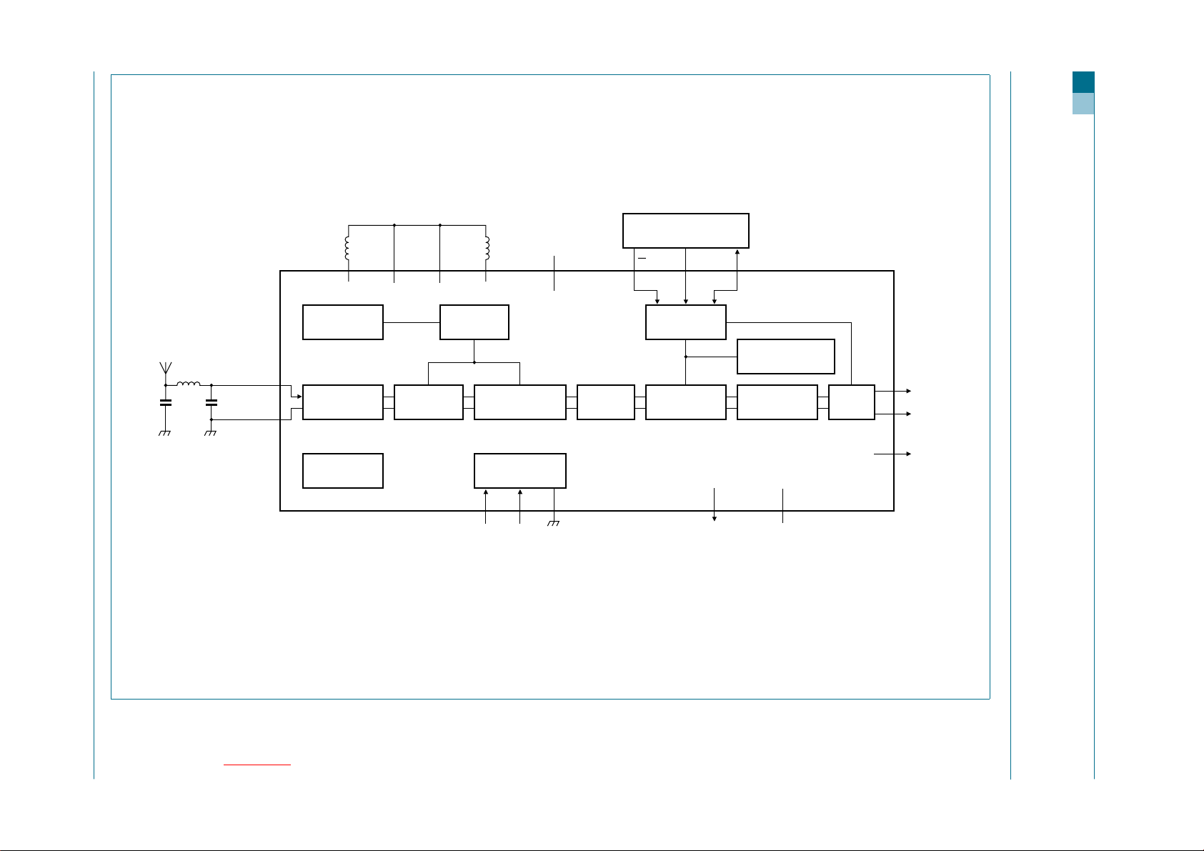
5. Block diagram
Philips Semiconductors
RFIN
RFGND
QUADRATURE
OSCILLATOR
1
QUADRATURE
2
STABILISATOR
MIXER
SELECTIVITY DEMODULATOR
TUNING
SYSTEM
V
CCA
POWER
SWITCH
5
V
CCD
DIGITAL
INTERFACE
STEREO
DECODER
DE-EMPHASIS
50/75 µs
TEA5880TS
4 3, 13, 24
GND LED n.c.
12 14, 15, 16, 22, 23
LEVEL VOLTAGE
GENERATOR
DE-EMPHASIS
15 kHz
MIXER
001aaa665
10
AUDL
11
AUDR
9
MPX
Fig 1. Block diagram.
Depending on the antenna design the filter components at pins 1 and 2 may not be necessary.The only two remaining coils connected to pin
17 to 20 can be replaced by printed-circuit board traces that will fit underneath the TEA5880TS resulting in a design without any external
components; see Section 14 for details on the printed-circuit board coils.
Integrated FM stereo radio IC for host processor tuning
TEA5880TS
Page 5
9397 750 13022 © Koninklijke Philips Electronics N.V. 2004. All rights reserved.
Preliminary data sheet Rev. 02 — 26 April 2004 5 of 27
xxxx xxxxxxxxxxxxxxxxxxxxxxxxxxxxxx x xxxxxxxxxxxxxx xxxxxxxxxx xxx xxxxxx xxxxxxxxxxxxxxxxxxxxxxx xxxxxxxxxxxxxxxxxxxxxx
xxxxx xxxxxx xx xxxxxxxxxxxxxxxxxxxxxxxxxxxxx xxxxxxxxxxxxxxxxxxxxxx xxxxxxxxxxx xxxxxxx xxxxxxxxxxxxxxxxxxx
xxxxxxxxxxxxxxxx xxxxxxxxxxxxxx xxxxxx xx xxxxxxxxxxxxxxxxxxxxxxxxxxxxxxxx xxxxxxxxxxxxxxxxxxxxxxxx xxxxxxx
xxxxxxxxxxxxxxxxxxxxxxxxxxxxxxxxxxxxxxxxxxxxxx xxxxxxxxxxx xxxxx x x
MICROCONTROLLER
LR1 V
CC1VCC1
LL1
reserved
2117 18 19 20
R/W CLOCK
68 7
DATA
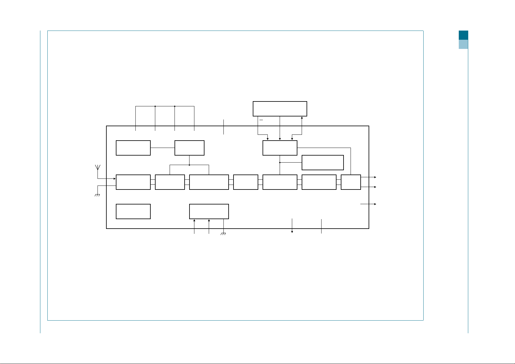
Philips Semiconductors
QUADRATURE
OSCILLATOR
RFIN
RFGND
QUADRATURE
MIXER
STABILISATOR
SELECTIVITY DEMODULATOR
Fig 2. Block diagram (no external components).
TUNING
SYSTEM
V
CCA
POWER
SWITCH
5
V
CCD
DIGITAL
INTERFACE
STEREO
DECODER
DE-EMPHASIS
50/75 µs
TEA5880TS
4 3, 13, 24
GND LED n.c.
12 14, 15, 16, 22, 23
LEVEL VOLTAGE
GENERATOR
DE-EMPHASIS
15 kHz
MIXER
001aaa666
10
AUDL
11
AUDR
9
MPX
Integrated FM stereo radio IC for host processor tuning
TEA5880TS
Page 6

Philips Semiconductors
6. Pinning information
6.1 Pin description
Table 3: Pin description
Symbol Pin Description
RFIN 1 RF input
RFGND 2 RF ground
GND 3 ground
V
CCD
V
CCA
R/W 6 digital read/write command input
DATA 7 bidirectional digital data line
CLOCK 8 digital data clock line input
MPX 9 FM MPX signal output
AUDL 10 audio left channel output
AUDR 11 audio right channel output
LED 12 stereo LED output
GND 13 ground
n.c. 14 not connected
n.c. 15 not connected
n.c. 16 not connected
LR1 17 coil right
V
CC1
V
CC1
LL1 20 coil left
reserved 21 reserved for testing use
n.c. 22 not connected
n.c. 23 not connected
GND 24 ground
TEA5880TS
Integrated FM stereo radio IC for host processor tuning
4 digital supply voltage
5 analog supply voltage
18 internal analog voltage
19 internal analog voltage
9397 750 13022 © Koninklijke Philips Electronics N.V. 2004. All rights reserved.
Preliminary data sheet Rev. 02 — 26 April 2004 6 of 27
Page 7
Philips Semiconductors
TEA5880TS
Integrated FM stereo radio IC for host processor tuning
Fig 3. Pin configuration.
7. Functional description
7.1 FM quadrature mixer
The FM quadrature mixer converts FM RF (76 MHz to 108 MHz) to an IF of 110 kHz. The
FM quadrature mixer provides inherent image rejection.
RFIN GND
1
RFGND n.c.
CLOCK LR1
2
GND n.c.
3
V
4
CCD
V
5
CCA
R/W V
6
7
8
9
10
11
12
TEA5880TS
001aaa667
DATA V
MPX n.c.
AUDL n.c.
AUDR n.c.
LED GND
24
23
22
21
20
19
18
17
16
15
14
13
reserved
LL1
CC1
CC1
7.2 Quadrature oscillator
The internally tuned LC VCO provides the Local Oscillator (LO) signal for the FM
quadrature mixer. The VCO frequency range is 150 MHz to 217 MHz.
7.3 Selectivity
Fully integrated I and Q channel IF filter.
7.4 Demodulator
The FM quadrature demodulator is an integrated PLL demodulator.
7.5 Level voltage generator and analog-to-digital converter
The level voltage is analog-to-digital converted with 3 bits and output via the data line.
7.6 IF counter
The IF counter outputs a 16-bit count result via the data line.
7.7 Mute
The digital interface controls the audio mute and output level.
9397 750 13022 © Koninklijke Philips Electronics N.V. 2004. All rights reserved.
Preliminary data sheet Rev. 02 — 26 April 2004 7 of 27
Page 8
Philips Semiconductors
7.8 Stereo decoder
The PLL stereo decoder is adjustment free. The stereo decoder can be switched to mono
via the digital interface.
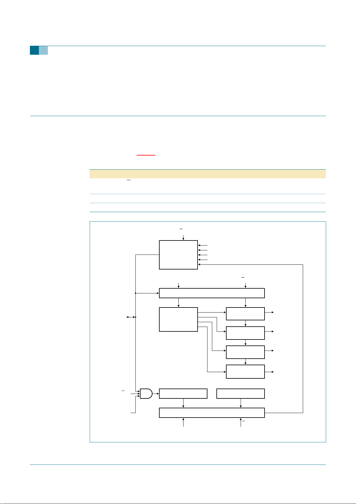
8. Digital interface (3-wire bus)
The TEA5880TS has a 3-wire bus with read/write, clock and data line.
The register set of the TEA5880TS can be accessed via the digital interface.
The pins given in Table 4 are defined for the digital interface of the TEA5880TS.
Table 4: Digital interface pins
Pin number Name Type Description Remark
Pin 6
Pin 8 CLOCK input clock rising edge
Pin 7 DATA input/output bidirectional data
R/W input LOW is read from TEA5880TS;
TEA5880TS
Integrated FM stereo radio IC for host processor tuning
HIGH is write to TEA5880TS
DATA
R/W
enable
counter 1
R/W
OUTPUT
SOURCE
SELECTOR
CLOCK
15 BITS SIPO (SERIAL IN PARALLEL OUT)
4 bits data
ADDRESS
DECODER
COUNTER 1 (16 bits)
16 bits data 16 bits data
16 BITS PISO (PARALLEL IN SERIAL OUT)
CLOCK R/W
stereo LED
stereo clock
IF OSC
FM OSC
REGISTER A
REGISTER B
REGISTER C
REST OF THE
REGISTERS
STATUS REGISTER
R/W
11 bits data
CONTROL
CONTROL
CONTROL
control bits
control bits
control bits
control bits
1-bit data
001aaa668
Fig 4. Digital interface block diagram.
9397 750 13022 © Koninklijke Philips Electronics N.V. 2004. All rights reserved.
Preliminary data sheet Rev. 02 — 26 April 2004 8 of 27
Page 9

Philips Semiconductors
8.1 Register description
Table 5: TEA5880TS registers description
Address Register name Access Operation Data width Clocks
0000b VADC write only VADC register 11 bits 15
0001b CTRL_C write only control register C 11 bits 15
0010b CTRL_A write only control register A 11 bits 15
0011b OSC_STEREO write only oscillator stereo
0100b CTRL_B write only control register B 11 bits 15
0101b CAP_FM write only capacitor bank FM 11 bits 15
0110b OSC_IF write only oscillator IF 11 bits 15
0111b OSC_FM write only oscillator FM 11 bits 15
- STATUS read only status register 16 bits 15
- COUNTER read only counter register 16 bits 15
Table 6: VADC - (address 0h) bit description
Bit Symbol Description
14 to 11 - address bits
10 to 6 VADC2[4:0] controls the width filter
5 - not applicable; should be written to logic 0
4 to 0 VADC1[4:0] controls the center filter
TEA5880TS
Integrated FM stereo radio IC for host processor tuning
11 bits 15
decoder clock
Table 7: CTRL_C - (address 1h) bit description
Bit Symbol Description
14 to 11 - address bits
10 and 9 - reserved for production test; should be written to logic 0
8 - reserved for swapping counters1 and 2; should be written to logic 0
7 to 4 - not applicable; should be written to logic 0
3 to 1 - reserved for time delay selection (counter 2); application should keep
bits 3 to 1 at logic 0; see
0 - reserved for enable counter 2; should be written to logic 0
[1] The application should write logic 0 to this register at start-up to ensure that the device functions correctly.
Table 8: Time delay selection
Value Decimal Stop value
000b 0 count 2
001b 1 count 8
010b 2 count 32
011b 3 count 128
100b 4 count 512
101b 5 count 2048
110b 6 count 8192
111b 7 count 32768
[1]
Table 8
9397 750 13022 © Koninklijke Philips Electronics N.V. 2004. All rights reserved.
Preliminary data sheet Rev. 02 — 26 April 2004 9 of 27
Page 10

Philips Semiconductors
Table 9: CTRL_A - (address 2h) bit description
Bit Symbol Description
14 to 11 - address bits
10 to 7 OUTPUT_
6 STE_PMUTE mutes the stereo PLL when set to logic 1; this bit should be
5 DEM_PMUTE mutes the demodulator PLL when set to logic 1; this bit
4 STE_INT_OFF# turns off the stereo integrator loop when set to logic 0
3 EN_MEAS# enables measurement when set to logic 0
2 AMUTE mutes the audio when set to logic 1
1 FM enables the FM circuitry when set to logic 1
0 - reserved for AM circuitry; should be written to logic 0
Table 10: Description of OUTPUT_SELECT bits
Symbol Value Decimal Output selected
OS-NONE 0000b 0 no output selected
OS_FM_OSC 0001b 1 FM oscillator
OS_NA2 0010b 2 not defined
OS_CNT2_RDY_NA 0011b 3 reserved for counter 2 ready output
OS_NA4 0100b 4 not defined
OS_STEREO_DEC 0101b 5 stereo decoder clock
OS_NA6 0110b 6 not defined
OS_STEREO_LED 0111b 7 stereo LED
OS_NA8 1000b 8 not defined
OS_IF_OSC 1001b 9 IF oscillator
OS_INTERRUPT_NA 1010b 10 reserved for interrupt output
OS_PISO 1011b 11 PISO output (reading STATUS / COUNTER
OS_NA12 1100b 12 not defined
OS_RDS_NA 1101b 13 reserved for RDS output
OS_NA14 1110b 14 not defined
OS_NA15 1111b 15 not defined
SELECT[3:0]
TEA5880TS
Integrated FM stereo radio IC for host processor tuning
selects an internal circuit as output for measurement purpose;
Table 10
see
set during calibration of the stereo decoder clock and should be
cleared during normal operation
should be set during calibration of the IF frequency and should
be cleared during normal operation
register)
Table 11: OSC_STEREO - (address 3h) bit description
Bit Symbol Description
14 to 11 - address bits
10 to 0 SO[10:0] 11-bit digital-to-analog converter for adjusting the stereo decoder clock
[1] The frequency is decreased when increasing the content of this register.
9397 750 13022 © Koninklijke Philips Electronics N.V. 2004. All rights reserved.
Preliminary data sheet Rev. 02 — 26 April 2004 10 of 27
[1]
Page 11

Philips Semiconductors
Table 12: CTRL_B - (address 4h) bit description
Bit Symbol Description
14 to 11 - address bits
10 L_CNT latch counter: a transition from logic 1 to logic 0 will latch the
9 L_STS latch status: a transition from logic 1 to logic 0 will latch the STATUS
8 to 6 - reserved for output level control; should be written with 4 (100b);
5 DEEMP de-emphasis: logic 1 is 75 µs (USA), logic 0 is 50 µs (Europe, Japan)
4 PISO_CLR a transition from logic 1 to logic 0 will clear the PISO; the PISO should
3 CNT_RST a transition from logic 1 to logic 0 will clear both counter 1 and counter 2
2 CNT1_EN counter 1 enabled (counting mode) when set to logic 1
1 - should be written to logic 0
0 MONO mono mode when set to logic 1, stereo mode when set to logic 0
TEA5880TS
Integrated FM stereo radio IC for host processor tuning
COUNTER register into the PISO (reading the PISO hereafter will read
the COUNTER register)
register into the PISO (reading the PISO hereafter will read the STATUS
register)
Table 13
see
be clear before reading the STATUS/COUNTER register
Table 13: Description of output level control register bits
Value Decimal Output level
0000b 0 12 mV
0001b 1 20 mV
0010b 2 35 mV
0011b 3 60 mV
0100b 4 100 mV
0101b 5 170 mV
0110b 6 200 mV
Table 14: CAP_FM - (address 5h) bit description
Bit Symbol Description
14 to 11 - address bits
10 - reserved for capacitor extra current; this bit should be written to logic 1
by any access to the CAP_FM to ensure that the device functions
properly
9 to 8 - reserved, should be written to logic 0
7 to 0 FC[7:0] FM capacitor bank switches for adjusting the FM (RF) frequency in big
steps. Every bit, when set, will switch on a capacitor with a weight
according to its position i.e. bit 0 has weight 1, bit 1 has weight 2, bit 2
has weight 4 etc, bit 6 has weight 64, exceptforbit 7, which also has the
same weight as bit 6; there is thus only 71⁄2 effective bits; this means
that the value range 0 to 127 will switch on different capacitors the value
range 128 to 191 switches on the same capacitors as range 64 to 127,
the value range 192 to 255 will switch on different capacitors (an
overlapped range of 64 values caused when FC[7:6] = 01b or 10b)
[1]
[1] The frequency is decreased when increasing the content of this register (more capacitors).
9397 750 13022 © Koninklijke Philips Electronics N.V. 2004. All rights reserved.
Preliminary data sheet Rev. 02 — 26 April 2004 11 of 27
Page 12

Philips Semiconductors
TEA5880TS
Integrated FM stereo radio IC for host processor tuning
Table 15: OSC_IF - (address 6h) bit description
[1]
Bit Symbol Description
14 to 11 - address bits
10 to 0 IFO[10:0] 11-bit digital-to-analog converter for adjusting the IF frequency
[1] The frequency is decreased when increasing the content of this register.
Table 16: OSC_FM - (address 7h) bit description
[1]
Bit Symbol Description
14 to 11 - address bits
10 to 0 FO[10:0] 11-bit digital-to-analog converter for adjusting the FM frequency in fine steps;
this register is used in combination with the CAP_FM register to set a FM
frequency
[1] The frequency is increased when increasing the content of this register.
Table 17: STATUS - bit description
[1]
Bit Symbol Description
15 to 9 FS[6:0] field strength, indicated by the amount of bits set:
0 bits set = < 10 dBµV
1 bit set = 10 dBµV to 20 dBµV
2 bits set = 20 dBµV to 30 dBµV
3 bits set = 30 dBµV to 40 dBµV
4 bits set = 40 dBµV to 50 dBµV
5 bits set = 50 dBµV to 60 dBµV
6 bits set = 60 dBµV to 70 dBµV
7 bits set = > 70 dBµV
8 - not applicable; always read as logic 1
7 to 5 R[2:0] chip revision; the revision for TEA5880TS is 100b
4 to 3 - not applicable; always read as logic 1
2 - reserved for production test
1 - not applicable; always read as logic 1
0 - reserved for production test
[1] This register does not have an address. To read the status register, latch its content into the PISO (using
L_STS bit in control register B) then read out the PISO.
Table 18: COUNTER - bit description
[1]
Bit Symbol Description
15 to 0 CNT[15:0] pulses counted during the period that the counter is enabled and the NR/W
line the 3 wire bus is low
[1] This register does not have an address. To read the counter register, latch its content into the PISO (using
L_CNT bit in control register B) then read out the PISO.
9397 750 13022 © Koninklijke Philips Electronics N.V. 2004. All rights reserved.
Preliminary data sheet Rev. 02 — 26 April 2004 12 of 27
Page 13

Philips Semiconductors
8.2 Accessing the TEA5880TS
Access to the TEA5880TS can be achieved via the 3-wire bus. At the host side, the R/W
and CLOCK are output signals, while the DATA signal is bidirectional.
When powered up, the host should initialize the 3-wire bus in the host read mode as
follows:
1. Set (at host side) the DATA line into input mode
2. R/W set to LOW
3. CLOCK set to LOW.
Note: Use the following sequence for changing read/write mode:
1. To change from host read mode to host write mode proceed as follows:
a. Keep the CLOCK signal LOW
b. Set the R/W signal to HIGH (write mode)
c. Set the DATA pin (of the application controller) into output mode.
2. To change from host write mode to host read mode proceed as follows:
a. Keep the CLOCK signal LOW
b. Set the DATA pin (of the application controller) into input mode
c. Set R/W to LOW (input mode).
TEA5880TS
Integrated FM stereo radio IC for host processor tuning
8.3 Writing to the TEA5880TS
Writing to the TEA5880TS is achieved with a 15-bit data pattern:
• D[14:11]: 4-bit register address
• D[10:0]: 11-bit register data.
The data pattern is sent serially to the TEA5880TS as follows:
1. Drive R/W pin HIGH to set the TEA5880TS in input mode
2. Drive the DATA pin to correct level
3. Generate positive edge of CLOCK (driving CLOCK into LOW-to-HIGH transition)
4. Delay some time to meet the data hold time requirement
5. Driving CLOCK into HIGH-to-LOW transition
6. Repeat step (2) to (5) 15 times to shift the 15-bit data pattern into the TEA5880TS
7. Drive R/W pin LOW; this signals the TEA5880TS to latch the data into the correct
register.
Note: The application should shift the LSB out first.
9397 750 13022 © Koninklijke Philips Electronics N.V. 2004. All rights reserved.
Preliminary data sheet Rev. 02 — 26 April 2004 13 of 27
Page 14

Philips Semiconductors
8.4 Reading from the TEA5880TS
Only the status or the counter register can be read from the TEA5880TS.
These are 16-bit registers and can be read serially as follow:
1. Select OS_PISO (parallel in, serial out) as output (control register A,
OUTPUT_SELECT bits)
2. Clear the PISO (control register B, PISO_CLR bit, pulse HIGH-to-LOW transition)
3. Latch the counter register (control register B, L_CNT bit, pulse HIGH-to-LOW
transition) or the status register (control register B, L_STS bit, pulse HIGH-to-LOW
transition) into the PISO
4. Drive R/W pin LOW to set the TEA5880TS in output mode
5. Read the first bit at pin DATA
6. Generate positive CLOCK pulse (LOW-to-HIGH transition)
7. Delay for a period of time to meet the data set-up time requirement
8. Read the data bit at pin DATA
9. Drive CLOCK into HIGH-to-LOW transition
10.Repeat step (6) to (9) 15 times to shift the remaining 15 bits of data out of the chip
TEA5880TS
Integrated FM stereo radio IC for host processor tuning
Note: The TEA5880TS will shift the MSB out first.
8.5 Measuring frequency with the TEA5880TS
The three frequencies: IF, stereo decoder clock and FM can be measured by using the
counter register and a software timing window. This is achieved as follows:
1. Select the output to be measured (control register A, OUTPUT_SELECT bits, select
OS_STEREO_DEC, OS_IF_OSC or OS_FM_OSC output)
2. Enable measure mode (clear EN_MEAS# bit of control register A)
3. Reset the counter (control register B, CNT_RST bit, pulse HIGH-to-LOW transition)
4. Start the counter on the TEA5880TS (control register B, set CNT1_EN bit); at the
moment the R/W signal goes LOW the counter starts
5. Wait time t
6. To stop the counter, first set the R/W signal HIGH, then disable the counter in the
TEA5880TS (control register B, clear CNT1_EN bit)
7. Read the pulse count n from the counter register of the TEA5880TS
8. Restore the measure mode
9. Restore the output select bits.
Note: The measuring window begins at the moment the R/W signal is driven LOW (point
4) and ends when the R/W signal is driven HIGH (point 6).
9397 750 13022 © Koninklijke Philips Electronics N.V. 2004. All rights reserved.
Preliminary data sheet Rev. 02 — 26 April 2004 14 of 27
Page 15

Philips Semiconductors
The IF and stereo decoder frequency can be calculated using the equation f = n/t, and the
FM frequency can be calculated using the equation f = (n/t) x 256.
Note: The precision of ‘f’ depends on the following:
• The duration of t. 1 pulse wrong at t = 1 ms results in more deviation than at t = 32 ms
• The precision of the measuring window: calculate with t = 32 ms gives other ‘f’ values
than with t = 32 ms. In the application care should be taken to have an accurate
measuring window t.
8.6 Initialize the TEA5880TS
After power-up, the TEA5880TS needs to be initialized as follows:
• Control register A: STE_PMUTE = 1; DEM_PMUTE = 1; AMUTE = 1; FM = 1; other
bits = 0
• Control register B: CNT_RST = 1; PISO_CLR = 1; MONO = 1; DEEMP = 1 (for
Europe); Bit [8:6] = 100b; other bits = 0
• Control register C: All bits = 0
• VADC register: VADC1 = 26 (decimal), this value should not be changed hereafter;
VADC2 = 18 (decimal), this value should not be changed hereafter
• Calibrate the IF frequency at 110 kHz
• Calibrate the stereo decoder clock at 37.5 kHz (to reduce the initialization time,
calibration of the stereo decoder clock can be postponed until the stereo mode is
selected).
TEA5880TS
Integrated FM stereo radio IC for host processor tuning
9. Timing diagrams
R/W
CLOCK
1 1511
LSB MSB MSBLSB
DATA
Fig 5. Writing data.
11-bit data 4-bit address
001aaa669
9397 750 13022 © Koninklijke Philips Electronics N.V. 2004. All rights reserved.
Preliminary data sheet Rev. 02 — 26 April 2004 15 of 27
Page 16

Philips Semiconductors
R/W
CLOCK
0 15
LSB
DATA
Fig 6. Reading data.
enable FM OSC at output source selector
TEA5880TS
Integrated FM stereo radio IC for host processor tuning
MSB
16-bit data
001aaa670
enable internet clock
set 16-bit counter clear
reset 16-bit counter clear
enable 16-bit counter to count
timing width 8 ms to 100 ms
disable 16-bit counter
enable PISO at output source
Fig 7. Measuring sequence.
001aaa671
9397 750 13022 © Koninklijke Philips Electronics N.V. 2004. All rights reserved.
Preliminary data sheet Rev. 02 — 26 April 2004 16 of 27
Page 17

Philips Semiconductors
TEA5880TS
Integrated FM stereo radio IC for host processor tuning
10. Limiting values
Table 19: Limiting values
In accordance with the Absolute Maximum Rating System (IEC 60134).
Symbol Parameter Conditions Min Max Unit
V
CCD
V
CCA
T
stg
T
amb
V
esd
[1] Machine model (R = 10 Ω, C = 200 pF, 75 µH).
[2] Human body model (R = 1.5 kΩ, C = 100 pF).
digital supply voltage −0.3 +5 V
analog supply voltage −0.3 +8 V
storage temperature −55 +150 °C
ambient temperature V
electrostatic discharge voltage
for all pins
V
CCA
CCA
= V
= V
CC(VCO)
CC(VCO)
= V
= V
= 3 V −10 +75 °C
CCD
= 5 V −40 +85 °C
CCD
[1]
−200 +200 V
[2]
−2000 +2000 V
11. Thermal characteristics
Table 20: Thermal characteristics
Symbol Parameter Conditions Typ Unit
R
th(j-a)
thermal resistance from junction to ambient in free air <tbd> K/W
12. Characteristics
Table 21: Digital input AC values
Symbol Parameter Conditions Min Typ Max Unit
Digital inputs
V
IH
V
IL
Digital outputs
I
sink (L)
V
OL
Timing
f
clk
t
CLK(H)
t
CLK(L)
HIGH-level input voltage IOH = 500 µA 1.4 - - V
LOW-level input voltage - - 0.6 V
LOW-level sink current 500 - - µA
LOW-level output voltage IOL = 500 µA - - 0.6 V
clock input - - 1 MHz
clock HIGH time 495 - - ns
clock LOW time 495 - - ns
9397 750 13022 © Koninklijke Philips Electronics N.V. 2004. All rights reserved.
Preliminary data sheet Rev. 02 — 26 April 2004 17 of 27
Page 18

Philips Semiconductors
TEA5880TS
Integrated FM stereo radio IC for host processor tuning
20
dB
(1)
0
−20
−40
−60
−10 1107030
(1) Mono signal.
(2) Mono noise.
(3) Stereo left.
(4) Stereo right.
(5) Stereo noise.
Fig 8. Signal characteristics.
001aaa673
(2)
(3)
(4)
(5)
RFIN (dBµV)
Fig 9. Total harmonic distortion.
13. Components list
No external components necessary.
THD = 30 %.
5
THD
(%)
4
3
2
1
0
−10 1107030
001aaa674
RFIN (dBµV)
9397 750 13022 © Koninklijke Philips Electronics N.V. 2004. All rights reserved.
Preliminary data sheet Rev. 02 — 26 April 2004 18 of 27
Page 19

Philips Semiconductors
Integrated FM stereo radio IC for host processor tuning
14. Printed-circuit board layout for SSOP24 package
TEA5880TS
The printed-circuit board traces from LL1 to V
and from V
CC1
to LR1 as shown in
CC1
Figure 10, are to create two inductors, each of approximately 38 nH. These inductors,
together with internal capacitors, form part of the LC oscillator to determine the FM tuning
band. If the value of the inductors becomes much greater than 38 nH, the whole FM
tuning band (normally from 76 MHz to 108 MHz) will be shifted lower. If the value of the
inductors becomes much smaller than 38 nH, the whole FM tuning band (normally from
76 MHz to 108 MHz) will be shifted higher.
If the layout of the two inductance traces is not preferred, two SMD inductors can be used
to replace the two printed-circuit board inductance traces as an alternative. The layout of
the two SMD inductors should be as close to the pins as possible.
RFIN
RFGND
GND
V
CCD
V
CCA
R/W
DATA
CLOCK
MPX
AUDL
AUDR
LED
GND
n.c.
n.c.
reserved
LL1
LR1
n.c.
n.c.
n.c.
GND
V
CC1
V
CC1
3.5 mm
3.5 mm
(1) Width of printed-circuit board trace = 0.15 mm; spacing between printed-circuit board
trace = 0.15 mm.
(2) Pins 14, 15, 16, 21, 22 and 23 are not connected.
001aaa675
Fig 10. Printed-circuit board layout.
9397 750 13022 © Koninklijke Philips Electronics N.V. 2004. All rights reserved.
Preliminary data sheet Rev. 02 — 26 April 2004 19 of 27
Page 20

Philips Semiconductors
15. Application information
V
CCD
100 nF
FM antenna
(1)
TEA5880TS
Integrated FM stereo radio IC for host processor tuning
RFIN
V
CCA
R/W
DATA
CLOCK
MPX
AUDL
AUDR
LED
1
2
3
4
5
6
7
8
9
10
11
12
TEA5880FM
24
23
22
21
20
19
18
17
16
15
14
13
001aaa672
LL1
V
CC1
LR1
V
CC1
100 nF
(1)
(1) optional.
Fig 11. Application diagram.
9397 750 13022 © Koninklijke Philips Electronics N.V. 2004. All rights reserved.
Preliminary data sheet Rev. 02 — 26 April 2004 20 of 27
Page 21

Philips Semiconductors
16. Package outline
TEA5880TS
Integrated FM stereo radio IC for host processor tuning
SSOP24: plastic shrink small outline package; 24 leads; body width 5.3 mm
D
c
y
Z
24 13
A
2
A
pin 1 index
1
SOT340-1
E
H
E
Q
L
p
L
(A )
A
X
v M
A
A
3
θ
112
w M
b
e
DIMENSIONS (mm are the original dimensions)
UNIT A1A2A
Note
1. Plastic or metal protrusions of 0.2 mm maximum per side are not included.
A
max.
0.21
mm
2
OUTLINE
VERSION
SOT340-1 MO-150
0.05
1.80
1.65
IEC JEDEC JEITA
0.25
b
3
p
0.38
0.25
p
cD
0.20
8.4
0.09
8.0
REFERENCES
0 2.5 5 mm
scale
(1)E(1) (1)
5.4
0.65 1.25
5.2
eHELLpQZywv θ
7.9
7.6
1.03
0.63
detail X
0.9
0.7
EUROPEAN
PROJECTION
0.13 0.10.2
0.8
0.4
ISSUE DATE
99-12-27
03-02-19
o
8
o
0
Fig 12. Package outline.
9397 750 13022 © Koninklijke Philips Electronics N.V. 2004. All rights reserved.
Preliminary data sheet Rev. 02 — 26 April 2004 21 of 27
Page 22

Philips Semiconductors
17. Soldering
17.1 Introduction to soldering surface mount packages
This text gives a very brief insight to a complex technology. A more in-depth account of
soldering ICs can be found in our
(document order number 9398 652 90011).
There is no soldering method that is ideal for all surface mount IC packages. Wave
soldering can still be used for certain surface mount ICs, but it is not suitable for fine pitch
SMDs. In these situations reflow soldering is recommended.
17.2 Reflow soldering
Reflow soldering requires solder paste (a suspension of fine solder particles, flux and
binding agent) to be applied to the printed-circuit board by screen printing, stencilling or
pressure-syringe dispensing before package placement. Driven by legislation and
environmental forces the worldwide use of lead-free solder pastes is increasing.
Several methods exist for reflowing; for example, convection or convection/infrared
heating in a conveyor type oven. Throughput times (preheating, soldering and cooling)
vary between 100 and 200 seconds depending on heating method.
TEA5880TS
Integrated FM stereo radio IC for host processor tuning
Data Handbook IC26; Integrated Circuit Packages
Typical reflow peak temperatures range from 215 to 270 °C depending on solder paste
material. The top-surface temperature of the packages should preferably be kept:
• below 225 °C (SnPb process) or below 245 °C (Pb-free process)
– for all BGA, HTSSON..T and SSOP..T packages
– for packages with a thickness ≥ 2.5 mm
– for packages with a thickness < 2.5 mm and a volume ≥ 350 mm3 so called
thick/large packages.
• below 240 °C (SnPb process) or below 260 °C (Pb-free process) for packages with a
thickness < 2.5 mm and a volume < 350 mm3 so called small/thin packages.
Moisture sensitivity precautions, as indicated on packing, must be respected at all times.
17.3 Wave soldering
Conventional single wave soldering is not recommended for surface mount devices
(SMDs) or printed-circuit boards with a high component density, as solder bridging and
non-wetting can present major problems.
To overcome these problems the double-wave soldering method was specifically
developed.
If wave soldering is used the following conditions must be observed for optimal results:
• Use a double-wave soldering method comprising a turbulent wave with high upward
pressure followed by a smooth laminar wave.
• For packages with leads on two sides and a pitch (e):
– larger than or equal to 1.27 mm, the footprint longitudinal axis is preferred to be
parallel to the transport direction of the printed-circuit board;
9397 750 13022 © Koninklijke Philips Electronics N.V. 2004. All rights reserved.
Preliminary data sheet Rev. 02 — 26 April 2004 22 of 27
Page 23

Philips Semiconductors
– smaller than 1.27 mm, the footprint longitudinal axis must be parallel to the
The footprint must incorporate solder thieves at the downstream end.
• For packages with leads on four sides, the footprint must be placed at a 45° angle to
the transport direction of the printed-circuit board. The footprint must incorporate
solder thieves downstream and at the side corners.
During placement and before soldering, the package must be fixed with a droplet of
adhesive. The adhesive can be applied by screen printing, pin transfer or syringe
dispensing. The package can be soldered after the adhesive is cured.
Typical dwell time of the leads in the wave ranges from 3 to 4 seconds at 250 °C or
265 °C, depending on solder material applied, SnPb or Pb-free respectively.
A mildly-activated flux will eliminate the need for removal of corrosive residues in most
applications.
17.4 Manual soldering
Fix the component by first soldering two diagonally-opposite end leads. Use a low voltage
(24 V or less) soldering iron applied to the flat part of the lead. Contact time must be
limited to 10 seconds at up to 300 °C.
TEA5880TS
Integrated FM stereo radio IC for host processor tuning
transport direction of the printed-circuit board.
When using a dedicated tool, all other leads can be soldered in one operation within
2 to 5 seconds between 270 and 320 °C.
17.5 Package related soldering information
Table 22: Suitability of surface mount IC packages for wave and reflow soldering methods
Package
BGA, HTSSON..T
SSOP..T
DHVQFN, HBCC, HBGA, HLQFP, HSO, HSOP,
HSQFP, HSSON, HTQFP, HTSSOP, HVQFN,
HVSON, SMS
PLCC
LQFP, QFP, TQFP not recommended
SSOP, TSSOP, VSO, VSSOP not recommended
CWQCCN..L
[1] For more detailed information on the BGA packages refer to the
[2] All surface mount (SMD) packages are moisture sensitive. Depending upon the moisture content, the
[3] These transparent plastic packages are extremely sensitive to reflow soldering conditions and must on no
[1]
Soldering method
Wave Reflow
[3]
[3]
, LBGA, LFBGA, SQFP,
, TFBGA, USON, VFBGA
not suitable suitable
not suitable
[5]
, SO, SOJ suitable suitable
[8]
, PMFP
order a copy from your Philips Semiconductors sales office.
maximum temperature (with respect to time) and body size of the package, there is a risk that internal or
external package cracks may occur due to vaporization of the moisture in them (the so called popcorn
effect). For details, refer to the Drypack information in the
Packages; Section: Packing Methods
account be processed through more than one soldering cycle or subjected to infrared reflow soldering with
peak temperature exceeding 217 °C ± 10 °C measured in the atmosphere of the reflow oven. The package
body peak temperature must be kept as low as possible.
[9]
, WQCCN..L
[8]
.
not suitable not suitable
[4]
[5] [6]
[7]
(LF)BGA Application Note
Data Handbook IC26; Integrated Circuit
suitable
suitable
suitable
(AN01026);
[2]
9397 750 13022 © Koninklijke Philips Electronics N.V. 2004. All rights reserved.
Preliminary data sheet Rev. 02 — 26 April 2004 23 of 27
Page 24

Philips Semiconductors
[4] These packages are not suitable for wave soldering. On versions with the heatsink on the bottom side, the
solder cannot penetrate between the printed-circuit board and the heatsink. On versions with the heatsink
on the top side, the solder might be deposited on the heatsink surface.
[5] If wave soldering is considered, then the package must be placed at a 45° angle to the solder wave
direction. The package footprint must incorporate solder thieves downstream and at the side corners.
[6] Wave soldering is suitable for LQFP, QFP and TQFP packages with a pitch (e) larger than 0.8 mm; it is
definitely not suitable for packages with a pitch (e) equal to or smaller than 0.65mm.
[7] Wave soldering is suitable for SSOP, TSSOP, VSO and VSOP packages with a pitch (e) equal to or larger
than 0.65 mm; it is definitely not suitable for packages with a pitch (e) equal to or smaller than 0.5mm.
[8] Image sensor packages in principle should not be soldered. They are mounted in sockets or delivered
pre-mounted on flex foil. However, the image sensor package can be mounted by the client on a flex foil by
using a hot bar soldering process. The appropriate soldering profile can be provided on request.
[9] Hot bar soldering or manual soldering is suitable for PMFP packages.
TEA5880TS
Integrated FM stereo radio IC for host processor tuning
9397 750 13022 © Koninklijke Philips Electronics N.V. 2004. All rights reserved.
Preliminary data sheet Rev. 02 — 26 April 2004 24 of 27
Page 25

Philips Semiconductors
Integrated FM stereo radio IC for host processor tuning
TEA5880TS
18. Revision history
Table 23: Revision history
Document ID Release date Data sheet status Change notice Order number Supersedes
TEA5880_2 20040426 Preliminary data sheet - 9397 750 13022 -
9397 750 13022 © Koninklijke Philips Electronics N.V. 2004. All rights reserved.
Preliminary data sheet Rev. 02 — 26 April 2004 25 of 27
Page 26

Philips Semiconductors
19. Data sheet status
TEA5880TS
Integrated FM stereo radio IC for host processor tuning
Level Data sheet status
I Objective data Development This data sheet contains data from the objective specification for product development. Philips
II Preliminary data Qualification Thisdata sheet contains data fromthe preliminary specification. Supplementary data will bepublished
III Product data Production This data sheet contains data from the product specification. Philips Semiconductors reserves the
[1] Please consult the most recently issued data sheet before initiating or completing a design.
[2] The product status of the device(s) described in this data sheet may have changed since this data sheet was published. The latest information is available on the Internet at
URL http://www.semiconductors.philips.com.
[3] For data sheets describing multiple type numbers, the highest-level product status determines the data sheet status.
[1]
Product status
20. Definitions
Short-form specification — The data in a short-form specification is
extracted from a full data sheet with the same type number and title. For
detailed information see the relevant data sheet or data handbook.
Limiting values definition — Limiting values given are in accordance with
the Absolute Maximum Rating System (IEC 60134). Stress above one or
more of the limiting values may cause permanent damage to the device.
These are stress ratings only and operation of the device at these or at any
other conditions above those given in the Characteristics sections of the
specification is not implied. Exposure to limiting values for extended periods
may affect device reliability.
Application information — Applications that are described herein for any
of these products are for illustrative purposes only. Philips Semiconductors
make no representation or warranty that such applications will be suitable for
the specified use without further testing or modification.
[2] [3]
Definition
Semiconductors reserves the right to change the specification in any manner without notice.
at a later date.Philips Semiconductors reserves theright to change thespecificationwithout notice, in
order to improve the design and supply the best possible product.
right to make changes at any time in order toimprove the design, manufacturing and supply. Relevant
changes will be communicated via a Customer Product/Process Change Notification (CPCN).
21. Disclaimers
Life support — These products are not designed for use in life support
appliances, devices, or systems where malfunction of these products can
reasonably be expected to result in personal injury. Philips Semiconductors
customers using or selling these products for use in such applications do so
at their own risk and agree to fully indemnify Philips Semiconductors for any
damages resulting from such application.
Right to make changes — Philips Semiconductors reserves the right to
make changes in the products - including circuits, standard cells, and/or
software - described or contained herein in order to improve design and/or
performance. When the product is in full production (status ‘Production’),
relevant changes will be communicated via a Customer Product/Process
Change Notification (CPCN). Philips Semiconductors assumes no
responsibility or liability for the use of any of these products, conveys no
license or title under any patent, copyright, or mask work right to these
products, andmakes no representationsor warranties thatthese products are
free from patent,copyright, or mask workrightinfringement, unlessotherwise
specified.
22. Contact information
For additional information, please visit: http://www.semiconductors.philips.com
For sales office addresses, send an email to: sales.addresses@www.semiconductors.philips.com
9397 750 13022 © Koninklijke Philips Electronics N.V. 2004. All rights reserved.
Preliminary data sheet Rev. 02 — 26 April 2004 26 of 27
Page 27

Philips Semiconductors
23. Contents
TEA5880TS
Integrated FM stereo radio IC for host processor tuning
1 General description . . . . . . . . . . . . . . . . . . . . . . 1
2 Features . . . . . . . . . . . . . . . . . . . . . . . . . . . . . . . 1
3 Quick reference data . . . . . . . . . . . . . . . . . . . . . 2
4 Ordering information . . . . . . . . . . . . . . . . . . . . . 3
5 Block diagram . . . . . . . . . . . . . . . . . . . . . . . . . . 4
6 Pinning information. . . . . . . . . . . . . . . . . . . . . . 6
6.1 Pin description . . . . . . . . . . . . . . . . . . . . . . . . . 6
7 Functional description . . . . . . . . . . . . . . . . . . . 7
7.1 FM quadrature mixer . . . . . . . . . . . . . . . . . . . . 7
7.2 Quadrature oscillator . . . . . . . . . . . . . . . . . . . . 7
7.3 Selectivity . . . . . . . . . . . . . . . . . . . . . . . . . . . . . 7
7.4 Demodulator. . . . . . . . . . . . . . . . . . . . . . . . . . . 7
7.5 Level voltage generator and analog-to-digital
converter. . . . . . . . . . . . . . . . . . . . . . . . . . . . . . 7
7.6 IF counter . . . . . . . . . . . . . . . . . . . . . . . . . . . . . 7
7.7 Mute . . . . . . . . . . . . . . . . . . . . . . . . . . . . . . . . . 7
7.8 Stereo decoder. . . . . . . . . . . . . . . . . . . . . . . . . 8
8 Digital interface (3-wire bus). . . . . . . . . . . . . . . 8
8.1 Register description . . . . . . . . . . . . . . . . . . . . . 9
8.2 Accessing the TEA5880TS. . . . . . . . . . . . . . . 13
8.3 Writing to the TEA5880TS . . . . . . . . . . . . . . . 13
8.4 Reading from the TEA5880TS . . . . . . . . . . . . 14
8.5 Measuring frequency with the TEA5880TS . . 14
8.6 Initialize the TEA5880TS . . . . . . . . . . . . . . . . 15
9 Timing diagrams . . . . . . . . . . . . . . . . . . . . . . . 15
10 Limiting values. . . . . . . . . . . . . . . . . . . . . . . . . 17
11 Thermal characteristics. . . . . . . . . . . . . . . . . . 17
12 Characteristics. . . . . . . . . . . . . . . . . . . . . . . . . 17
13 Components list. . . . . . . . . . . . . . . . . . . . . . . . 18
14 Printed-circuit board layout for SSOP24
package. . . . . . . . . . . . . . . . . . . . . . . . . . . . . . . 19
15 Application information. . . . . . . . . . . . . . . . . . 20
16 Package outline. . . . . . . . . . . . . . . . . . . . . . . . 21
17 Soldering . . . . . . . . . . . . . . . . . . . . . . . . . . . . . 22
17.1 Introduction to soldering surface mount
packages . . . . . . . . . . . . . . . . . . . . . . . . . . . . 22
17.2 Reflow soldering. . . . . . . . . . . . . . . . . . . . . . . 22
17.3 Wave soldering. . . . . . . . . . . . . . . . . . . . . . . . 22
17.4 Manual soldering . . . . . . . . . . . . . . . . . . . . . . 23
17.5 Package related soldering information. . . . . . 23
18 Revision history . . . . . . . . . . . . . . . . . . . . . . . 25
19 Data sheet status. . . . . . . . . . . . . . . . . . . . . . . 26
20 Definitions . . . . . . . . . . . . . . . . . . . . . . . . . . . . 26
21 Disclaimers . . . . . . . . . . . . . . . . . . . . . . . . . . . 26
22 Contact information . . . . . . . . . . . . . . . . . . . . 26
© Koninklijke Philips Electronics N.V. 2004
All rights are reserved. Reproduction in whole or in part is prohibited without the prior
written consent of the copyright owner. The information presented in this document does
not form part of any quotation or contract, is believed to be accurate and reliable and may
be changed without notice. No liability will be accepted by the publisher for any
consequence of its use. Publication thereof does not convey nor imply any license under
patent- or other industrial or intellectual property rights.
Document order number: 9397 750 13022
Published in The Netherlands
Date of release: 26 April 2004
 Loading...