

Page 1

查询TEA1552供应商查询TEA1552供应商
INTEGRATED CIRCUITS
DATA SH EET
TEA1552
GreenChipII SMPS control IC
Product specification
Supersedes data of 2002 Jul 03
2002 Aug 27
Page 2

Philips Semiconductors Product specification
GreenChipII SMPS control IC TEA1552
FEATURES
Distinctive features
• Universal mains supply operation (70 to 276 V AC)
• High level of integration, giving a very low external
component count.
Green features
• Valley or zero voltage switching for minimum switching
losses
• Efficient quasi-resonant operation at high power levels
• Frequency reductionat low power standby for improved
system efficiency (<3 W)
• Cycle skipping mode at very low loads. Pi< 300 mW at
no-load operation for a typical adapter application
• On-chip start-up current source
• Standby indication pin to indicate low output power
consumption.
Protection features
• Safe restart mode for system fault conditions
• Continuous mode protection by means of
demagnetization detection (zero switch-on current)
• Accurate and adjustable overvoltage protection
(latched)
• Short winding protection
• Undervoltage protection (foldback during overload)
• Overtemperature protection (latched)
• Low and adjustable overcurrent protection trip level
• Soft (re)start
• Mains voltage-dependent operation-enabling level
• General purpose input for lock protection.
APPLICATIONS
Typical application areas are adapters and chargers (e.g.
for laptops, camcorders and printers) and all applications
that demand an efficient and cost-effective solution up to
250 W.
GENERAL DESCRIPTION
The GreenChip
(1)
II is the second generation of green
Switched Mode Power Supply (SMPS) control ICs
operatingdirectly from the rectified universalmains.A high
level of integration leads to a cost effective power supply
with a very low number of external components.
The special built-in green functions allow the efficiency to
be optimum at all power levels. This holds for
quasi-resonant operation at high power levels, as well as
fixed frequency operation with valley switching at medium
power levels. At low power (standby) levels, the system
operates at reduced frequency and with valley detection.
The proprietary high voltage BCD800 process makes
direct start-up possible from the rectified mains voltage in
an effective and green way. A second low voltage
BICMOS IC is used for accurate, high speed protection
functions and control.
Highly efficient, reliable supplies can easily be designed
using the GreenChipII control IC.
(1) GreenChip is a trademark of Koninklijke Philips
Electronics N.V.
2002 Aug 27 2
Page 3
Philips Semiconductors Product specification
GreenChipII SMPS control IC TEA1552
handbook, full pagewidth
VCOadj
I
sense
STDBY
DRIVER
HVS
HVS
DRAIN
1
2
3
4
TEA1552T
5
6
7
DEM
14
CTRL
13
LOCK
12
V
CC(5V)
11
GND
10
n.c.
9
V
CC
8
MBL498
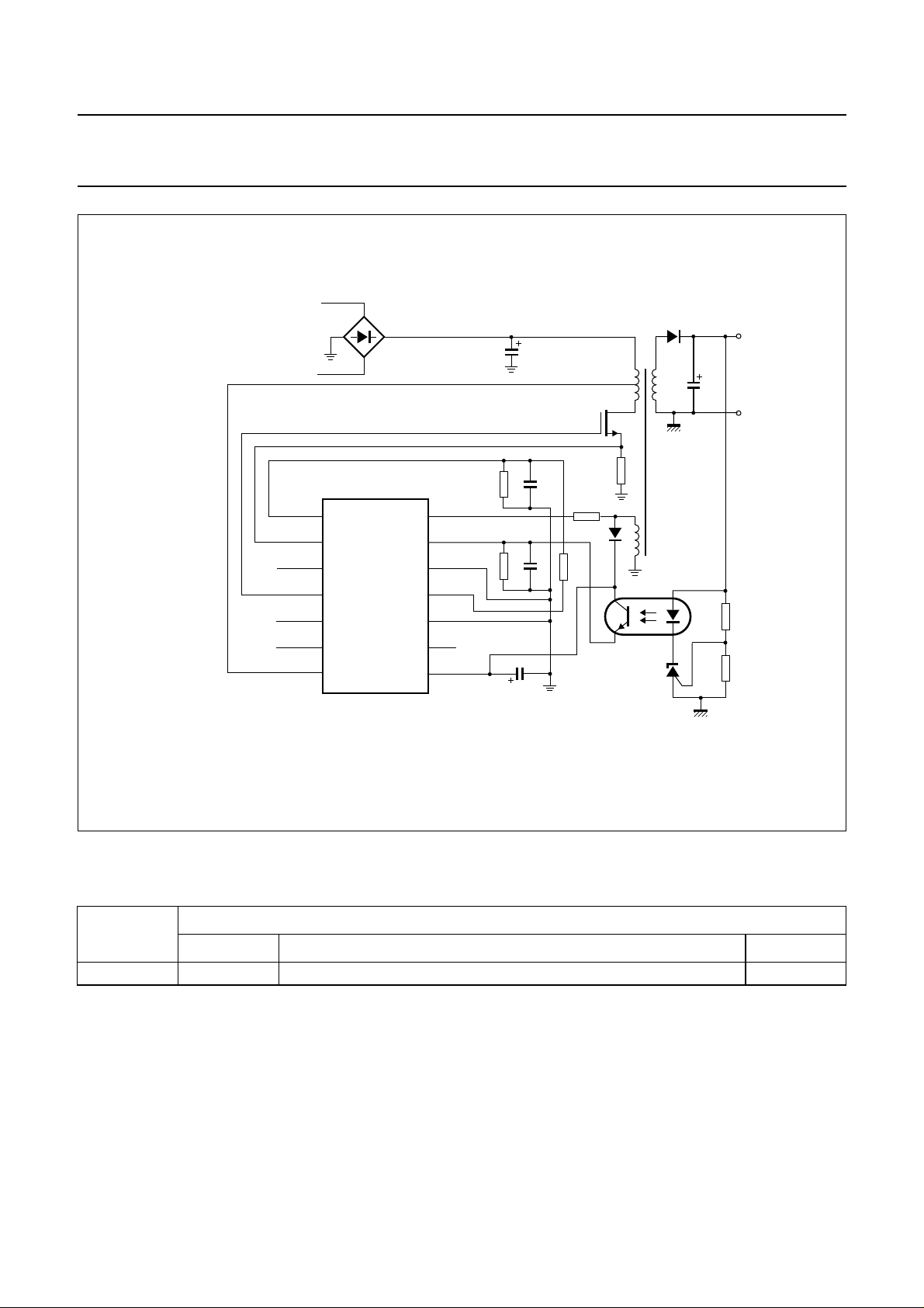
Fig.1 Basic application.
ORDERING INFORMATION
TYPE
NUMBER
NAME DESCRIPTION VERSION
PACKAGE
TEA1552T SO14 plastic small outline package; 14 leads; body width 3.9 mm SOT108-1
2002 Aug 27 3
Page 4
Philips Semiconductors Product specification
GreenChipII SMPS control IC TEA1552
BLOCK DIAGRAM
handbook, full pagewidth
V
CC
GND
STDBY
VCOadj
CTRL
LOCK
8
10
3
1
13
12
300 Ω
5.6 V
S1
TEA1552
2.5 V
M-level
lock
detect
FREQUENCY
CONTROL
−1
SUPPLY
MANAGEMENT
internal
supply
VOLTAGE
CONTROLLED
OSCILLATOR
POWER-ON
TEMPERATURE
PROTECTION
UVLO start
RESET
OVER-
V
CC
LOGIC
UVLO
MAXIMUM
ON-TIME
PROTECTION
< 4.5 V
LOGIC
SQ
R
Q
SQ
R
Q
START-UP
CURRENT SOURCE
VALLEY
100 mV
short
winding
OVER-POWER
PROTECTION
OVER-
VOLTAGE
PROTECTION
DRIVER
LEB
blank
OCP
0.88 V
clamp
soft
start
S2
5 V/1 mA
(max)
7
DRAIN
5, 6
HVS
14
DEM
4
DRIVER
I
ss
0.5 V
2
I
sense
11
V
CC(5V)
MBL499
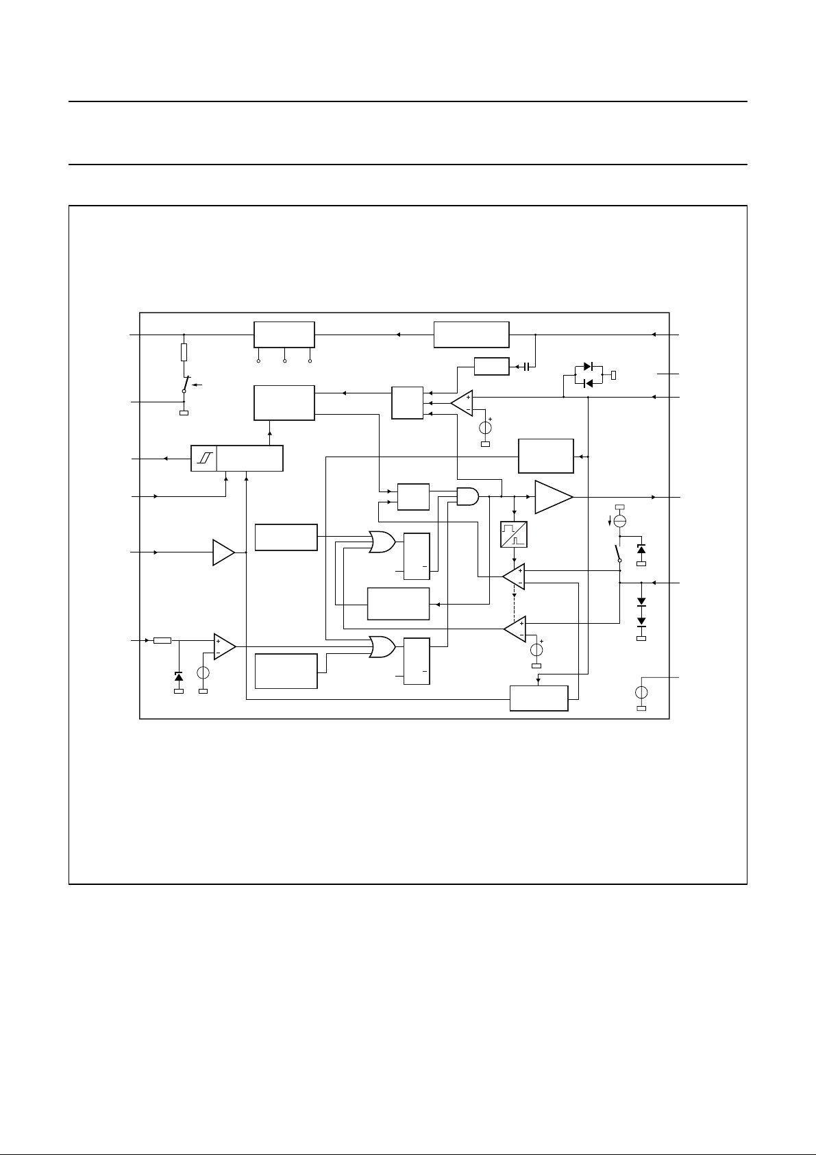
Fig.2 Block diagram.
2002 Aug 27 4
Page 5
Philips Semiconductors Product specification
GreenChipII SMPS control IC TEA1552
PINNING FUNCTIONAL DESCRIPTION
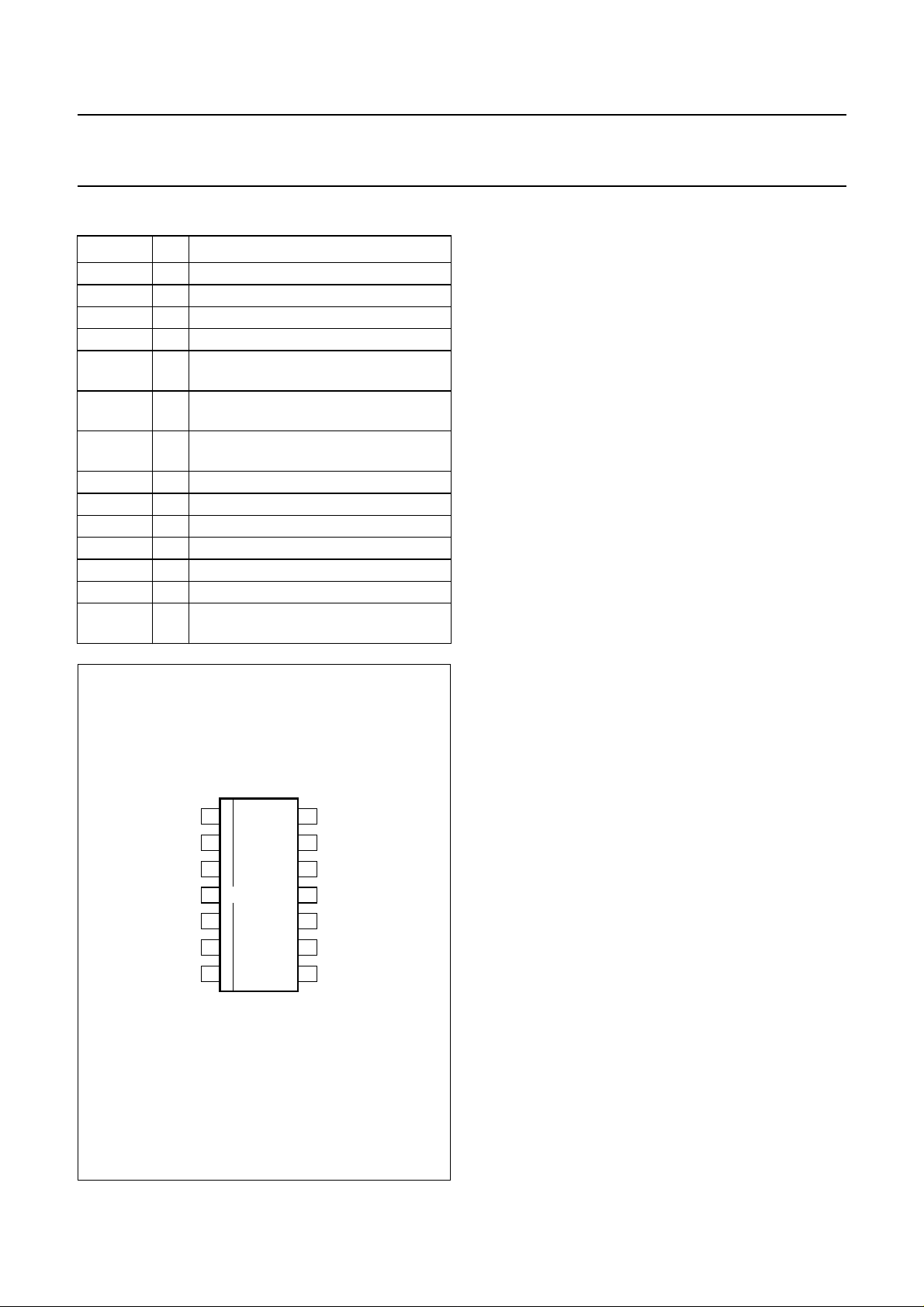
SYMBOL PIN DESCRIPTION
VCOadj 1 VCO adjustment input
I
sense
2 programmable current sense input
STDBY 3 standby indication or control output
DRIVER 4 gate driver output
HVS 5 high voltage safety spacer, not
connected
HVS 6 high voltage safety spacer, not
connected
DRAIN 7 drain of external MOS switch, input for
start-up current and valley sensing
V
CC
8 supply voltage
n.c. 9 not connected
GND 10 ground
V
CC(5V)
11 5 V output
LOCK 12 lock input
CTRL 13 control input
DEM 14 input from auxiliary winding for
demagnetization timing, OVP and OPP
The TEA1552 is the controller of a compact flyback
converter, with the IC situated at the primary side.
An auxiliary winding of the transformer provides
demagnetization detection and powers the IC after
start-up.
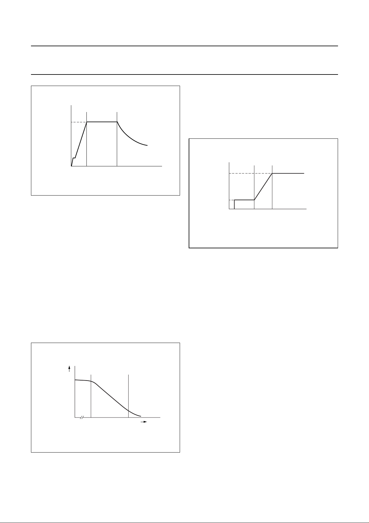
The TEA1552 operates in multi modes (see Fig.4).
The next converter stroke is started only after
demagnetization of the transformer current (zero current
switching), while the drain voltage has reached the lowest
voltage to prevent switching losses (green function). The
primary resonant circuit of primary inductance and drain
capacitor ensures this quasi-resonant operation. The
design can be optimized in such a way that zero voltage
switching can be reached over almost the complete
universal mains range.
To prevent very high frequency operation at lower loads,
the quasi-resonant operation changes smoothly in fixed
frequency PWM control.
At very low power (standby) levels, the frequency is
controlled down, via the VCO, to a minimum frequency of
approximately 25 kHz.
Start-up, mains enabling operation level and
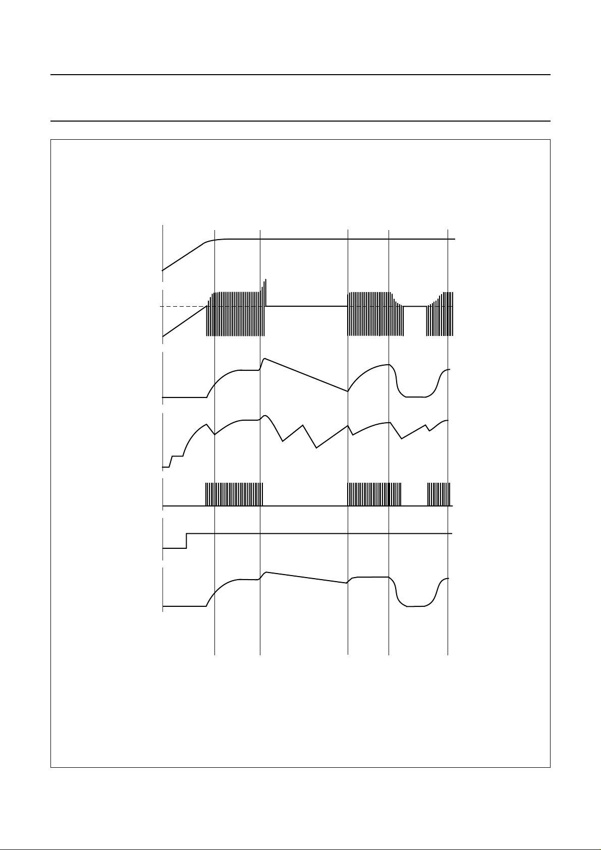
undervoltage lock-out (see Figs 11 and 12)
handbook, halfpage
VCOadj
STDBY
DRIVER
I
sense
HVS
HVS
DRAIN
1
2
3
4
TEA1552T
5
6
7
Fig.3 Pin configuration.
MBL497
Initially, the IC is self supplying from the rectified mains
voltage via pin DRAIN. Supply capacitor C
is charged
VCC
by the internal start-up current source to a level of
approximately 4 V or higher, depending on the drain
DEM
14
13
CTRL
12
LOCK
11
V
CC(5V)
GND
10
n.c.
9
V
8
CC
voltage. Once the drain voltage exceeds the M-level
(mains-dependent operation-enabling level), the start-up
current source will continue charging capacitor C
VCC
(switch S1 will be opened); see Fig.2. The IC will activate
the power converter as soon as the voltage on pin V
passes the level V
. The IC supply is taken over by
CC(start)
CC
the auxiliary winding as soon as the output voltage
reaches its intended level and the IC supply from the
mains voltage is subsequently stopped for high efficiency
operation (green function).
The moment the voltage on pin VCC drops below the
undervoltage lock-out level V
, the IC stops switching
UVLO
and enters a safe restart from the rectified mains voltage.
Inhibiting the auxiliary supply by external means causes
the converter to operate in a stable, well defined burst
mode.
Supply management
All (internal) reference voltages are derived from a
temperature compensated, on-chip band gap circuit.
2002 Aug 27 5
Page 6
Philips Semiconductors Product specification
GreenChipII SMPS control IC TEA1552
The maximum fixed frequency of the oscillator isset by an
internal current source and capacitor. The maximum
frequency is reduced once the control voltage enters the
VCO control window. Then, the maximum frequency
changeslinearly with thecontrol voltage untilthe minimum
frequency is reached (see Figs 5 and 6).
handbook, halfpage
(kHz)
f
VCO fixed quasi resonant
125
MBL500
25
P (W)
Fig.4 Multi mode operation.
Current mode control
Current mode control is used for its good line regulation
behaviour.
The ‘on-time’ iscontrolled by theinternally inverted control
pin voltage, which is compared with the primary current
information. The primary current is sensed across an
external resistor. The driver output is latched in the logic,
preventing multiple switch-on.
The internal control voltage is inverselyproportional to the
external control pin voltage, with an offset of 1.5 V. This
means that a voltage range from 1 to 1.5 V on pin CTRL
will result in an internal control voltage range from
0.5 to 0 V (a high external control voltage results in a low
duty cycle).
Oscillator
V
handbook, halfpage
sense(max)
0.52 V
MGU233
handbook, halfpage
f
(kHz)
125
25
VCO
VCO
level
1
2
level
Fig.6 VCO frequency as a function of V
MBL501
125 kHz
V
sense(max) (V)
sense(max)
.
VCO adjustment
The VCOadj pin can be used to set the VCO operation
point. As soon as the peak voltageon thesense resistoris
controlledbelow half thevoltage on the VCOadjpin (VCO
level), frequency reduction will start. The actual peak
voltageonsense will be somewhat higherduetoswitch-off
delay (see Fig.7). The frequency reduction will stop
approximately 25 mV lower (VCO2 level), when the
minimum frequency is reached.
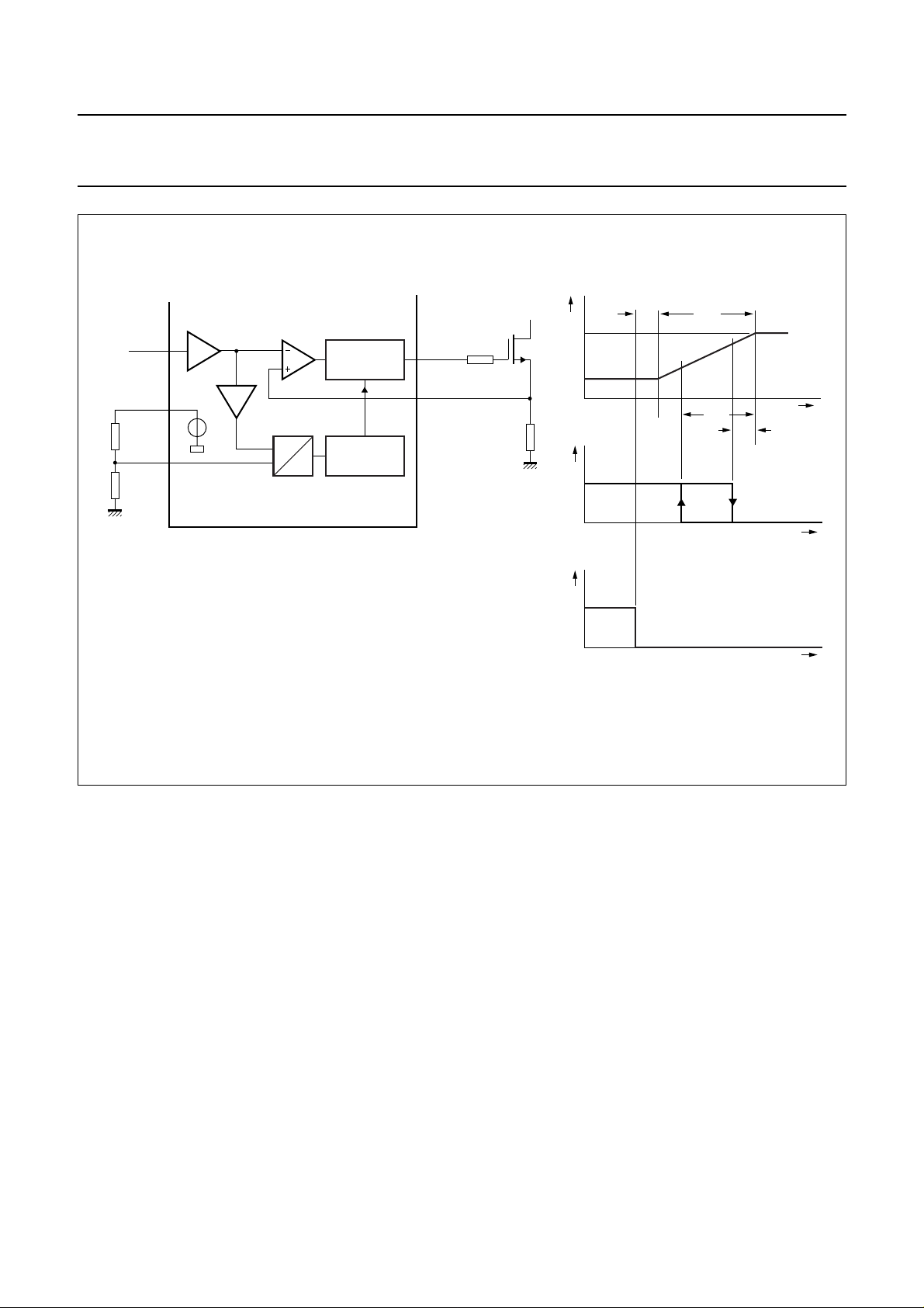
Cycle skipping
At very low power levels, a cycle skipping mode will be
activated. A high control voltage will reduce the switching
frequency to a minimum of 25 kHz. If the voltage on the
controlpin has raisedeven more, switch-onof the external
power MOSFET will be inhibited until the voltage on the
control pin has dropped to a lower value again (see Fig.7).
1
V
CTRL
CTRL
.
Fig.5 V
1 V
(typ)
sense(max)
1.5 V
(typ)
as a function of V
2002 Aug 27 6
For system accuracy, it is not the absolute voltage on the
control pin that will trigger the cycle skipping mode, but a
signal derived from the internal VCO will be used.
Remark: If the no-load requirement of the system is such
that the output voltage can be regulated to its intended
level at a switching frequency of 25 kHz or above, the
cycle skipping mode will not be activated.
Page 7
Philips Semiconductors Product specification
GreenChipII SMPS control IC TEA1552
handbook, full pagewidth
1.5 V − V
CTRL
CTRL
V
CC(5V)
VCOadj
The voltage levels dV1,dV2,dV3and dV4are fixed in the IC to typically 50 mV, 18 mV, 40 mV and 15 mV respectively.
The level at which VCO mode of operation starts or ends can be externally controlled with the VCOadj pin.
X2
5 V
V
x
current
comparator
V
I
DRIVER
OSCILLATOR
DRIVER
I
sense
MBL502
f
osc
f
max
f
min
V
STDBY
(V)
5
0
cycle
skipping
1
0
dV
2
dV
dV
1
4
VCO
Vx (mV)
adj
Vx (mV)
Vx (mV)
3
dV
Fig.7 A functional implementation of the standby and cycle skipping circuitry.
Standby output
TheSTDBY output pin (V
= 5 V)can be used to drive
STDBY
an external NPN transistor or FET in order to e.g.
switch-off a PFCcircuit. The STDBY output is activated by
the internal VCO: as soon as the VCO has reduced the
switching frequency to (almost) the minimum frequency of
25 kHz, the STDBY output will be activated (see Fig.7).
The STDBY output will go low again as soon as the VCO
allows a switching frequency close to the maximum
frequency of 125 kHz.
Demagnetization
The system will be in discontinuous conduction mode all
the time. The oscillator will not start a new primary stroke
until the secondary stroke has ended.
Demagnetization features a cycle-by-cycle output
short-circuit protection by immediately lowering the
frequency (longer off-time), thereby reducing the power
level.
Demagnetizationrecognition is suppressedduringthe first
time (t
). This suppression may be necessary in
suppr
applications where the transformer has a large leakage
inductance and at low output voltages/start-up.
OverVoltage Protection (OVP)
An OVP mode is implemented in the GreenChip series.
For the TEA1552, this works by sensing the auxiliary
voltage via the current flowing into pin DEM during the
secondary stroke. The auxiliary winding voltage is a
well-defined replica of the output voltage. Any voltage
spikes are averaged by an internal filter.
If the output voltage exceeds the OVP trip level, the OVP
circuit switches off the power MOSFET. The controller
then waits until the UVLO level is reached on pin VCC.
When VCC drops to UVLO, capacitor C
recharged to the V
level, however the IC will not start
start
VCC
will be
switching again. Subsequently, VCC will drop again to the
UVLO level, etc.
2002 Aug 27 7
Page 8
Philips Semiconductors Product specification
GreenChipII SMPS control IC TEA1552
Operation only recommenceswhen the VCCvoltage drops
below a level of approximately 4.5 V (practically when the
V
has been disconnected for a short period).
mains
The output voltage (V
can be set by the demagnetization resistor R
N
V
OVP
where N
s
-----------N
is the number of secondary turnsand N
s
I
aux
) at which the OVP function trips,
OVP
R
OVP DEM()
+×[]×=
DEMVclamp DEM()pos()
DEM
:
aux
is the
number of auxiliary turns of the transformer.
Current I
OVP(DEM)
The value of the demagnetization resistor (R
is internally trimmed.
DEM
) can be
adjusted to the turns ratio of the transformer, thus making
an accurate OVP possible.
handbook, full pagewidth
primary
stroke
secondary
stroke
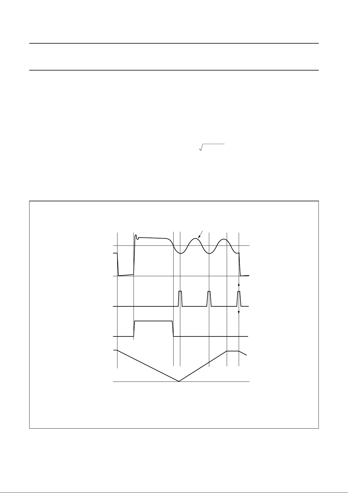
Valley switching (see Fig.8)
A new cycle starts when the power switch is switched on.
After the ‘on-time’ (which is determined by the ‘sense’
voltage and the internal control voltage), the switch is
opened and the secondary stroke starts.
After the secondary stroke, the drain voltage shows an
oscillation with a frequency of approximately
---------------------------------------------------2π×L
where L
1
C
×()×()
p
d
is the primary self inductance of the transformer
p
and Cd is the capacitance on the drain node.
secondary
ringing
drain
valley
secondary
stroke
oscillator
A: Start of new cycle at lowest drain voltage.
B: Start of new cycle in a classical PWM system at high drain voltage.
Fig.8 Signals for valley switching.
BA
MGU235
2002 Aug 27 8
Page 9

Philips Semiconductors Product specification
GreenChipII SMPS control IC TEA1552
As soon as the oscillator voltage is high again and the
secondary stroke has ended, the circuit waits for the
lowest drain voltage before starting a new primary stroke.
This method is called valley detection. Figure 8 shows the
drain voltage together with the valley signal, the signal
indicating the secondary stroke and the oscillator signal.
In an optimum design, the reflected secondary voltage on
the primary side will force the drain voltage to zero. Thus,
zero voltage switching is very possible, preventing large
1
capacitive switching losses , and
P
-- -
2
2
CV
f×××=
allowing high frequency operation, which results in small
and cost effective inductors.
MGU236
handbook, halfpage
−100 µA
(typ)
I
DEM
−24 µA
(typ)
V
sense(max)
0.52 V
(typ)
0.3 V
(typ)
OverCurrent Protection (OCP)
The cycle-by-cycle peak drain current limit circuit uses the
externalsource resistor to measurethecurrent accurately.
This allows optimum size determination of the transformer
core (cost issue). The circuit is activated after the leading
edge blanking time t
. The OCP protection circuit limits
leb
the ‘sense’ voltage to an internal level.
OverPower Protection (OPP)
Duringthe primary stroke,the rectified mainsinput voltage
is measured by sensing the current drawn from pin DEM.
This current is dependent on the mains voltage, according
to the following formula:
N
where:
N
=
-----------N
aux
p
V
aux
≈≈
I
-------------- -
DEM
R
DEM
×
NV
mains
-------------------------R
DEM
The current information is used to adjust the peak drain
current, which is measured via pin I
. The internal
sense
compensation is such that an almost mains independent
maximum output power can be realized.
The OPP curve is given in Fig.9.
Fig.9 OPP correction curve.
Minimum and maximum ‘on-time’
The minimum ‘on-time’ of the SMPS is determined by the
Leading Edge Blanking (LEB) time. The IC limits the
‘on-time’ to 50 µs. When the system desires an ‘on-time’
longer than 50 µs,a fault condition is assumed,and the IC
will stop switching and enter the safe restart mode.
Short winding protection
After the leading edge blanking time, the short winding
protection circuit is also activated. If the ‘sense’ voltage
exceeds the short winding protection voltage V
swp
, the
converter will stop switching. Once VCC drops below the
UVLO level, capacitor C
will be recharged and the
VCC
supply will restart again. This cycle will be repeated until
the short-circuit is removed (safe restart mode).
The short winding protection will also protect in case of a
secondary diode short-circuit.
2002 Aug 27 9
Page 10
Philips Semiconductors Product specification
GreenChipII SMPS control IC TEA1552
LOCK input
Pin LOCK is a general purpose (high-impedance) input
pin, which can be used to switch off the IC. As soon as the
voltageonthis pin is raised above 2.5 V,switchingwillstop
immediately.Thevoltage on the VCCpinwillcycle between
V
CC(start)
and V
CC(UVLO)
, but the IC will not start switching
again until the latch function is reset. The latch is reset as
soon as the VCC drops below 4.5 V (typical value). The
internal OVP and OTP will also trigger this latch (see
Fig.2).
The detection levelof this inputis related to the V
voltage in the following way: 0.5 × V
CC(5V)
± 4%.
CC(5V)
pin
An internal Zener diode clamp of 5.6 V will protect this pin
from excessive voltages. No internal filtering is done on
this input.
OverTemperature Protection (OTP)
An accurate temperature protection is provided in the
circuit. When the junction temperature exceeds the
thermal shutdown temperature, the IC will stop switching.
When VCC drops to UVLO, capacitor C
recharged to the V
level, however the IC will not start
start
VCC
will be
switching again. Subsequently, VCC will drop again to the
UVLO level, etc.
Operation only recommences when theVCCvoltage drops
below a level of approximately 4.5 V (practically when the
V
has been disconnected for a short period).
mains
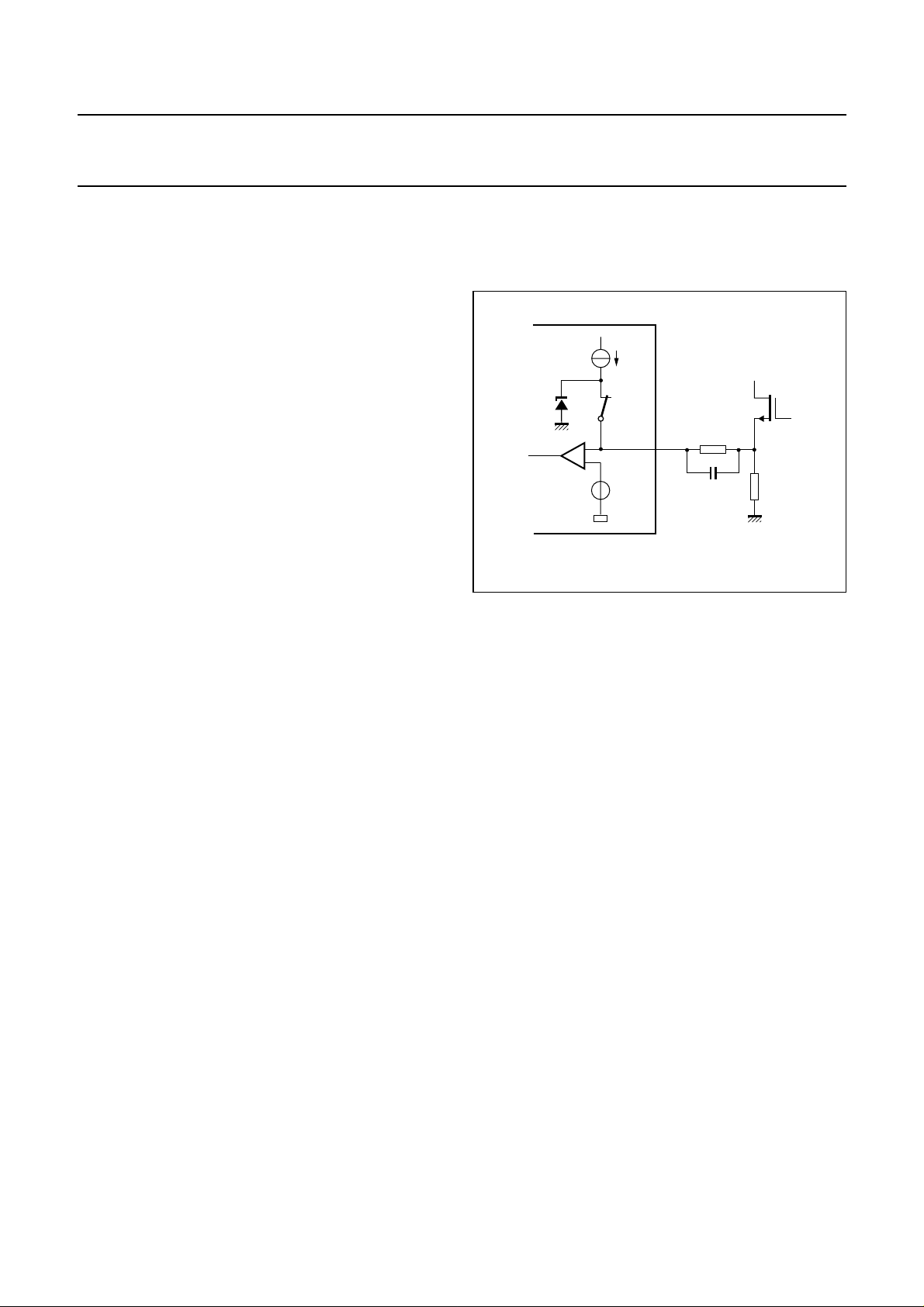
Soft start-up
To prevent transformer rattle during hiccup, the
transformer peak current is slowly increased by the soft
start function. This can be achieved by inserting a resistor
and a capacitor between pin I
and the sense resistor
sense
(see Fig.10). An internal current source charges the
capacitor to V = ISS× RSS, with a maximum of
approximately 0.5 V.
The start level and the time constant of the increasing
primary current level can be adjusted externally by
changing the values of RSS and CSS.
I
primary(max)
τ R
SSCSS
V
ocpISSRSS
=
---------------------------------------------- -
×=
×()–
R
sense
Since the soft start current I
is subtracted from pin V
SS
CC
chargingcurrent, the RSSvaluewill affect the VCCcharging
current level by a maximum of 60 µA (typical value).
handbook, halfpage
I
SS
0.5 V
start-up
V
ocp
2
I
sense
R
SS
C
SS
R
sense
MBL503
Fig.10 Soft start-up.
5 V output
Pin V
can be used for supplying external circuitry.
CC(5V)
The maximum output current must be limited to 1 mA.
If higher peak currents are required, an external RC
combination should limit the current drawn from this pin to
1 mA maximum.
The 5 V output voltage will be available as soon as the
start-upvoltage is reached.As the highvoltage supply can
not supply the 5 V pin during start-up and/or shutdown,
during latched shutdown (via pin LOCK or other latched
protection such as OVP or OTP), the voltage is switched
to zero.
Driver
The driver circuit to the gate of the power MOSFET has a
current sourcing capability of typically 170 mA and a
current sink capability of typically 700 mA. This permits
fast turn-on andturn-off of thepower MOSFET for efficient
operation. A low driver source current has been chosen to
limit the ∆V/∆t at switch-on. Thisreduces Electro Magnetic
Interference (EMI) and also limits the current spikes
across R
sense
.
The charging currentI
pin I
pin I
is below approximately 0.5 V. If the voltage on
sense
exceeds 0.5 V, the soft start current source will
sense
start limiting the current ISS. At the V
will flow aslong as the voltage on
SS
level, the I
CC(start)
SS
current source is completely switched off.
2002 Aug 27 10
Page 11
Philips Semiconductors Product specification
GreenChipII SMPS control IC TEA1552
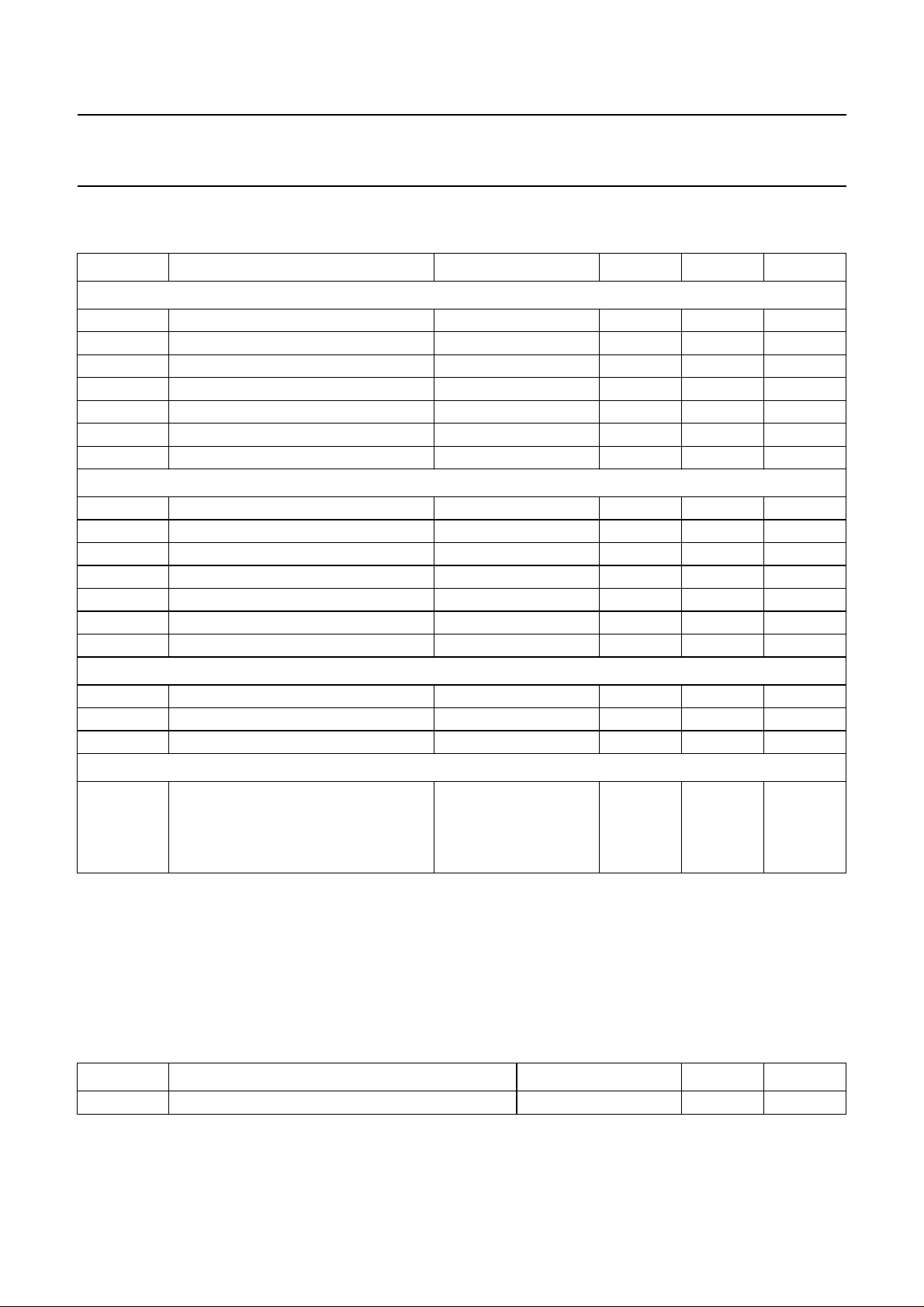
LIMITING VALUES
In accordance with the Absolute Maximum Rating System (IEC 60134); note 1.
SYMBOL PARAMETER CONDITIONS MIN. MAX. UNIT
Voltages
V
VCOadj
V
sense
V
DRAIN
V
CC
V
LOCK
V
CTRL
V
DEM
Currents
I
sense
I
STDBY
I
DRIVER
I
DRAIN
I
CC(5V)
I
CTRL
I
DEM
General
P
tot
T
stg
T
j
ESD
V
esd
voltage on pin VCOadj continuous −0.4 +5 V
voltage on pin I
sense
current limited −0.4 − V
voltage on pin DRAIN −0.4 +650 V
supply voltage continuous −0.4 +20 V
voltage on pin LOCK continuous −0.4 +7 V
voltage on pin CTRL −0.4 +5 V
voltage on pin DEM current limited −0.4 − V
current on pin I
sense
−1 +10 mA
current on pin STDBY −1 − mA
current on pin DRIVER d < 10% −0.8 +2 A
current on pin DRAIN − +5 mA
current on pin V
CC(5V)
−10 mA
current on pin CTRL − +5 mA
current on pin DEM −250 +250 µA
total power dissipation T
<70°C − 0.75 W
amb
storage temperature −55 +150 °C
junction temperature −20 +145 °C
electrostatic discharge voltage
pins 1 to 6 and pins 9 to 14 HBM class 1; note 2 − 2000 V
pin 7 HBM class 1; note 2 − 1500 V
any other pin MM; note 3 − 400 V
Notes
1. All voltages are measured with respect to ground; positive currents flow into the chip; pin VCC may not be current
driven. The voltage ratings are valid provided other ratings are not violated; current ratings are valid provided the
maximum power rating is not violated.
2. Equivalent to discharging a 100 pF capacitor through a 1.5 kΩ series resistor.
3. Equivalent to discharging a 200 pF capacitor through a 0.75 µH coil and a 10 Ω resistor.
THERMAL CHARACTERISTICS
SYMBOL PARAMETER CONDITIONS VALUE UNIT
R
th(j-a)
thermal resistance from junction to ambient in free air; note 1 100 K/W
Note
1. With pin GND connected to sufficient copper area on the printed-circuit board.
2002 Aug 27 11
Page 12
Philips Semiconductors Product specification
GreenChipII SMPS control IC TEA1552
QUALITY SPECIFICATION
In accordance with
‘SNW-FQ-611D’
.
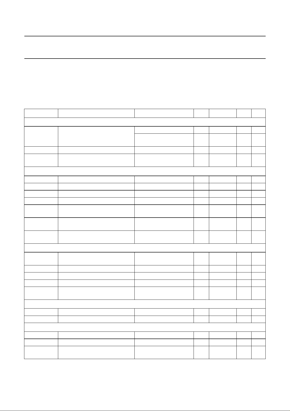
CHARACTERISTICS
T
=25°C; VCC= 15 V; all voltages are measured with respect to ground; currents are positive when flowing into
amb
the IC; unless otherwise specified.
SYMBOL PARAMETER CONDITIONS MIN. TYP. MAX. UNIT
Start-up current source (pin DRAIN)
I
DRAIN
BV
DSS
supply current from pin DRAIN VCC=0V; V
breakdown voltage 650 −−V
M-level mains-dependent
with auxiliary supply;
V
DRAIN
> 100 V
> 100 V 1.0 1.2 1.4 mA
DRAIN
− 100 300 µA
60 − 100 V
operation-enabling level
Supply voltage management (pin V
V
CC(start)
V
CC(UVLO)
V
CC(hys)
I
CC(h)
I
CC(l)
I
CC(restart)
I
CC(oper)
start-up voltage on V
undervoltage lock-out on V
hysteresis voltage on V
pin VCC charging current (high) V
pin VCC charging current (low) V
pin VCC restart current V
supply current under normal
CC
CC
)
CC
CC
10.3 11 11.7 V
8.1 8.7 9.3 V
V
CC(start)
DRAIN
DRAIN
3V<VCC<V
DRAIN
V
CC(UVLO)<VCC
− V
CC(UVLO)
2.0 2.3 2.6 V
> 100 V; VCC<3V −1.2 −1 −0.8 mA
> 100 V;
> 100 V;
CC(UVLO)
<V
CC(start)
−1.2 −0.75 −0.45 mA
−650 −550 −450 µA
no load on pin DRIVER 1.1 1.3 1.5 mA
operation
Demagnetization management (pin DEM)
V
th(DEM)
demagnetization comparator
50 100 150 mV
threshold voltage on pin DEM
I
prot(DEM)
V
clamp(DEM)(neg)
V
clamp(DEM)(pos)
t
suppr
protection current on pin DEM V
negative clamp voltage on pin DEM I
positive clamp voltage on pin DEM I
suppression of transformer ringing
=50mV −50
DEM
= −150 µA −0.5 −0.25 −0.05 V
DEM
= 250 µA 0.5 0.7 0.9 V
DEM
(1)
−−10 nA
1.1 1.5 1.9 µs
at start of secondary stroke
Pulse width modulator
t
on(min)
t
on(max)
minimum on-time − t
leb
maximum on-time latched 40 50 60 µs
− ns
Oscillator
f
osc(l)
f
osc(h)
V
vco(start)
oscillator low fixed frequency V
oscillator high fixed frequency V
peak voltage on pin I
sense
, where
> 1.5 V 20 25 30 kHz
CTRL
< 1 V 100 125 150 kHz
CTRL
see Figs 6 and 7 − VCO
1
− mV
frequency reduction starts
2002 Aug 27 12
Page 13
Philips Semiconductors Product specification
GreenChipII SMPS control IC TEA1552
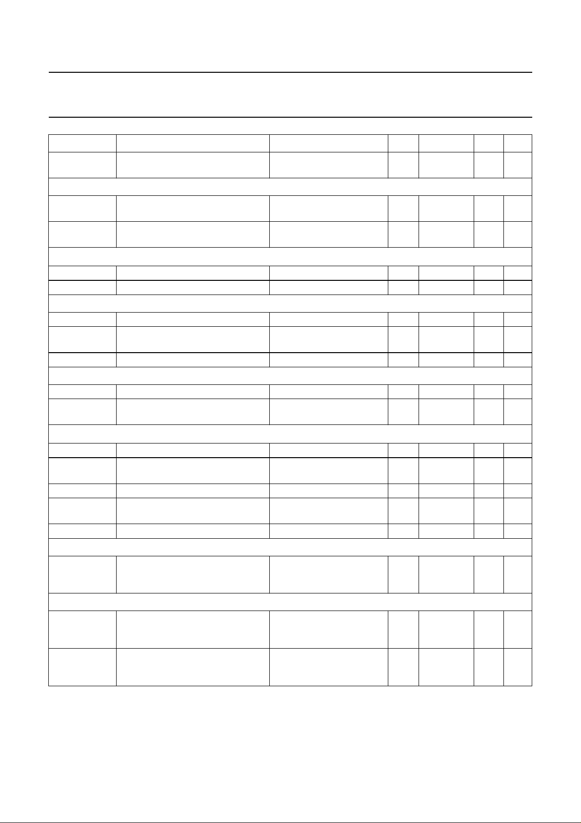
SYMBOL PARAMETER CONDITIONS MIN. TYP. MAX. UNIT
V
vco(max)
Duty cycle control (pin CTRL)
V
CTRL(min)
V
CTRL(max)
5 V output (pin V
V
CC(5V)
I
CC(5V)
LOCK input (pin LOCK)
V
LOCK
V
CC(reset)
REL
LOCK,5V
Valley switch (pin DRAIN)
∆V/∆t
valley
t
valley-swon
Overcurrent and short winding protection (pin I
V
sense(max)
t
PD
V
swp
t
leb
I
SS
Overvoltage protection (pin DEM)
I
OVP(DEM)
Overpower protection (pin DEM)
I
OPP(DEM)
I
OPP50%(DEM)
peak voltage on pin I
the frequency is equal to f
minimum voltage on pin CTRL for
sense
, where
osc(l)
− VCO1− 25 − mV
− 1.0 − V
maximum duty cycle
maximum voltage on pin CTRL for
− 1.5 − V
minimum duty cycle
)
CC(5V)
output voltage IO= 1 mA 4.75 5.0 5.25 V
current capability of pin V
CC(5V)
−1.0 −−mA
LOCK trip level 2.37 2.5 2.63 V
voltage level on pin VCC which
V
< 2.3 V − 4.5 − V
LOCK
resets the latch
relation to 5 V output (pin V
CC(5V)
)V
LOCK
= 0.5 × V
CC(5V)
−4 − +4 %
valley recognition voltage change −85 −+85 V/µs
delay from valley recognition to
− 150
(1)
− ns
switch-on
)
sense
maximum source voltage OCP ∆V/∆t = 0.1 V/µs 0.48 0.52 0.56 V
propagation delay from detecting
V
sense(max)
to switch-off
∆V/∆t = 0.5 V/µs − 140 185 ns
short winding protection voltage 0.83 0.88 0.96 V
blanking time for current and short
300 370 440 ns
winding protection
soft start current V
OVP level on pin DEM set by resistor R
< 0.5 V 45 60 75 µA
sense
DEM
; see
54 60 66 µA
Section “OverVoltage
Protection (OVP)”
OPP current on pin DEM to start
OPP correction
set by resistor R
DEM
Section “OverPower
; see
−−24 −µA
Protection (OPP)”
OPP current on pin DEM, where
−−100 −µA
maximum source voltage is limited
to 0.3 V
2002 Aug 27 13
Page 14
Philips Semiconductors Product specification
GreenChipII SMPS control IC TEA1552
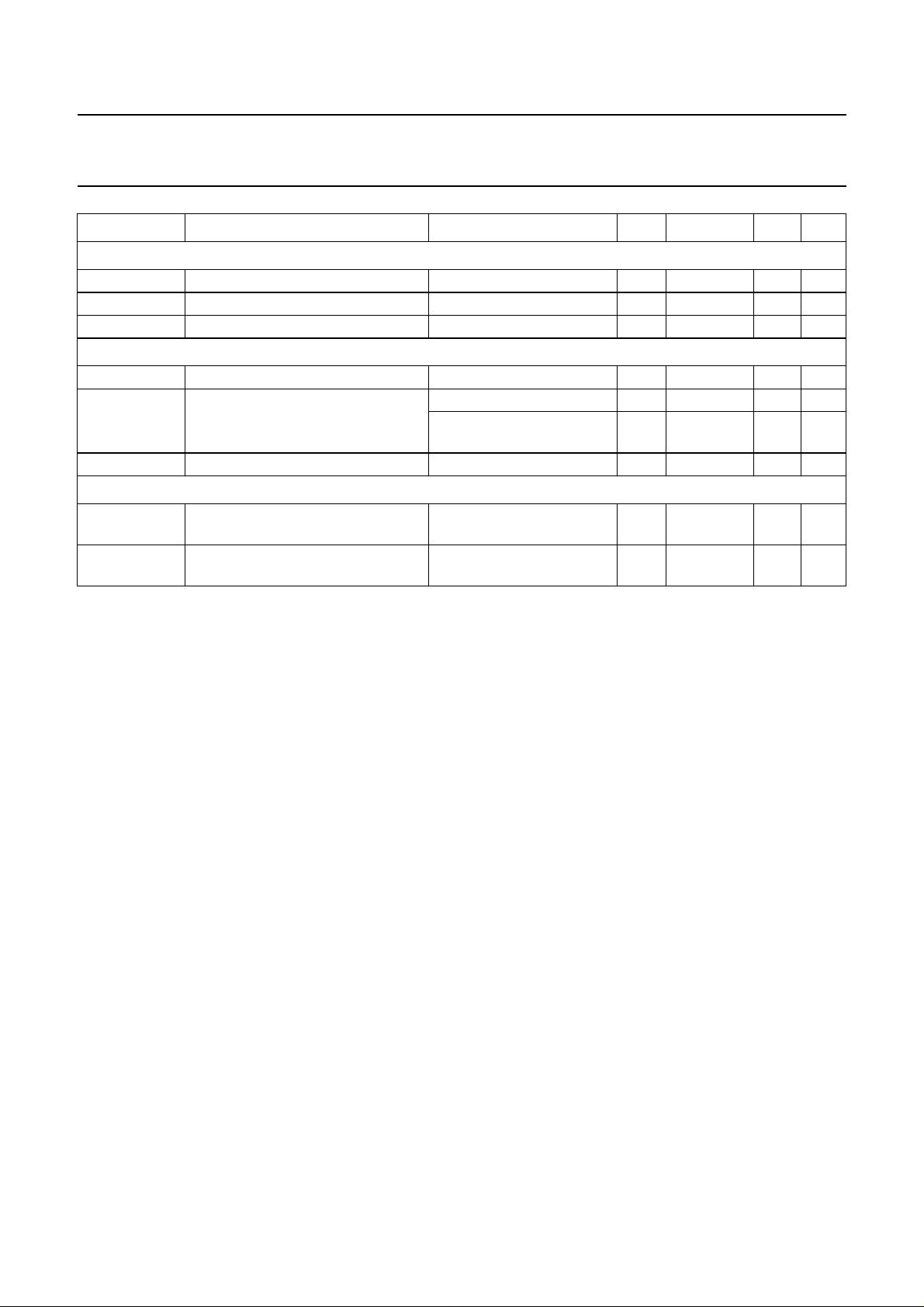
SYMBOL PARAMETER CONDITIONS MIN. TYP. MAX. UNIT
Standby output (pin STDBY)
V
STDBY
I
source
I
sink
Driver (pin DRIVER)
I
source
I
sink
V
o(driver)(max)
Temperature protection
T
prot(max)
T
prot(hys)
standby output voltage 4.75 5.0 5.25 V
source current capability V
sink current capability V
source current capability of driver VCC= 9.5 V; V
sink current capability of driver VCC= 9.5 V; V
V
V
=1V 20 22 24 µA
STDBY
=1V 2 −−mA
STDBY
=2V −−170 −88 mA
DRIVER
=2V − 300 − mA
DRIVER
= 9.5 V;
CC
DRIVER
= 9.5 V
400 700 − mA
maximum output voltage of driver VCC>12V − 11.5 12 V
maximum temperature protection
130 140 150 °C
level
hysteresis for the temperature
− 8
(1)
−°C
protection level
Note
1. Guaranteed by design.
2002 Aug 27 14
Page 15
Philips Semiconductors Product specification
GreenChipII SMPS control IC TEA1552
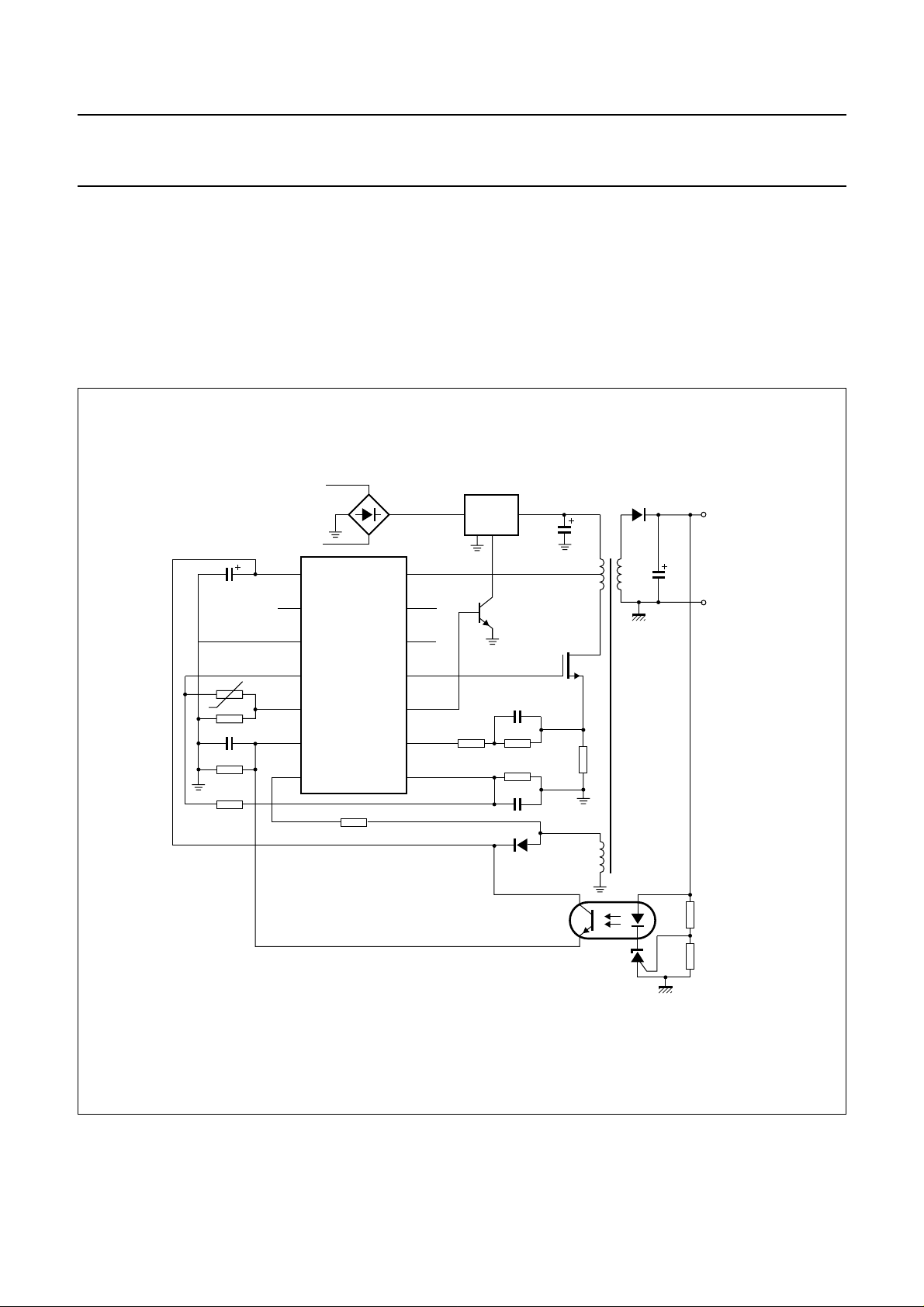
APPLICATION INFORMATION
A converter with the TEA1552 consistsof an inputfilter, a transformerwith a thirdwinding (auxiliary), andan output stage
with a feedback circuit.
Capacitor C
(at pin VCC) buffers the supply voltage of the IC, which is powered via the high voltage rectified mains
VCC
during start-up and via the auxiliary winding during operation.
A sense resistor converts the primary current into a voltage at pin I
maximum primary peak current.
V
CC(5V)
LOCK
CTRL
V
V
CC
n.c.
GND
DEM
mains
8
9
10
11
TEA1552T
12
13
14
7
6
5
4
3
2
1
DRAIN
HVS
HVS
DRIVER
STDBY
I
sense
VCOadj
PFC
Rs2
handbook, full pagewidth
C
−
C
CTRL
R
CTRL
VCC
t
. The value of this sense resistor defines the
sense
D
V
i
N
p
power
MOSFET
C
SS
R
SS
R
sense
o
N
s
V
o
C
o
R
DEM
The LOCKpinis used in this example foranadditional external overtemperature protection.
If this pin is not used, it must be tied to ground.
Fig.11 Configuration with controlled PFC.
2002 Aug 27 15
N
aux
R
reg1
R
reg2
MBL504
Page 16
Philips Semiconductors Product specification
GreenChipII SMPS control IC TEA1552
handbook, full pagewidth
V
i
V
D
(power
MOSFET)
V
V
CC
V
gate
M-level
V
µC
o
start-up
sequence
normal
operation
overvoltage
protection
normal
operation
output
short-circuit
MBL505
Fig.12 Typical waveforms.
2002 Aug 27 16
Page 17
Philips Semiconductors Product specification
GreenChipII SMPS control IC TEA1552
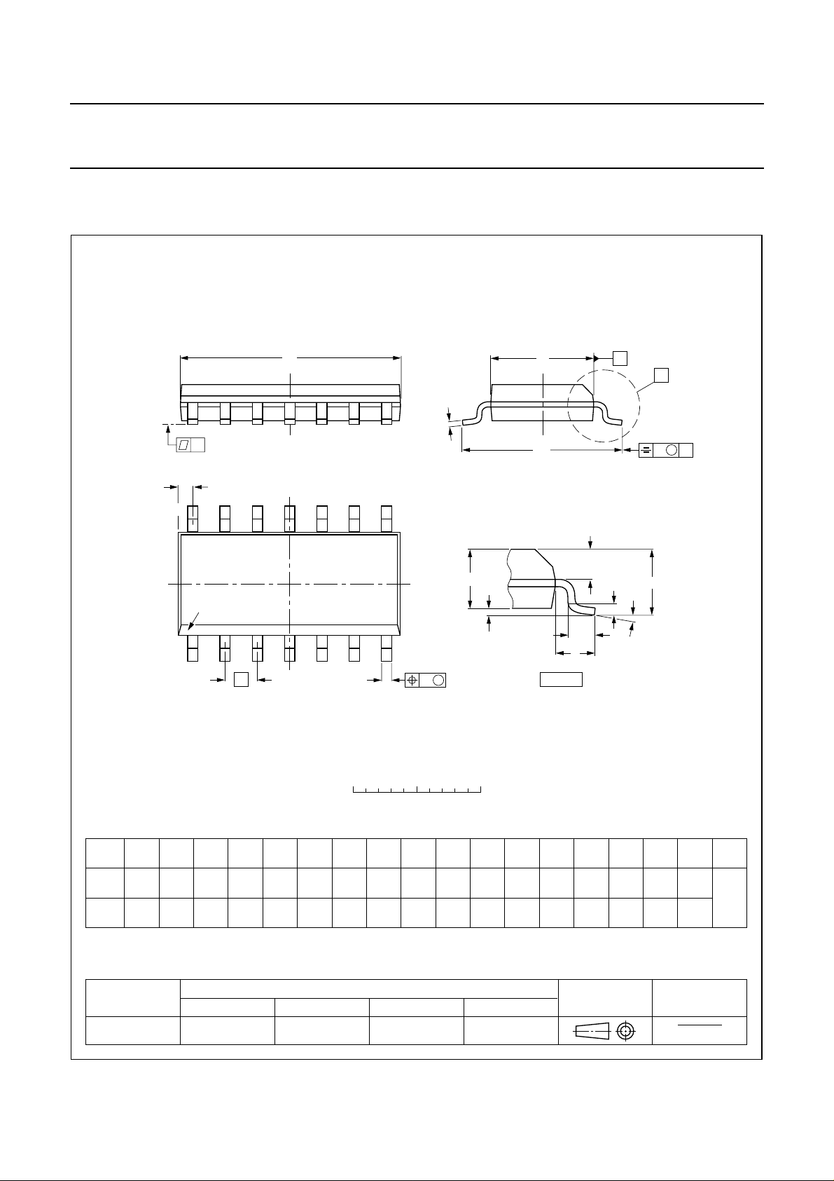
PACKAGE OUTLINE
SO14: plastic small outline package; 14 leads; body width 3.9 mm
SOT108-1
y
Z
14
pin 1 index
1
D
c
8
A
2
A
1
7
e
w M
b
p
E
H
E
detail X
A
X
v M
A
Q
(A )
L
p
L
A
3
θ
0 2.5 5 mm
scale
DIMENSIONS (inch dimensions are derived from the original mm dimensions)
mm
OUTLINE
VERSION
SOT108-1
A
max.
1.75
0.069
A
1
0.25
0.10
0.010
0.004
A2A
1.45
1.25
0.057
0.049
IEC JEDEC EIAJ
076E06 MS-012
0.25
0.01
b
3
p
0.49
0.25
0.36
0.19
0.019
0.0100
0.014
0.0075
UNIT
inches
Note
1. Plastic or metal protrusions of 0.15 mm maximum per side are not included.
(1)E(1)
cD
8.75
8.55
0.35
0.34
REFERENCES
4.0
3.8
0.16
0.15
1.27
0.050
2002 Aug 27 17
eHELLpQZywv θ
1.05
0.041
1.0
0.4
0.039
0.016
0.7
0.25
0.6
0.028
0.01 0.004
0.024
EUROPEAN
PROJECTION
0.25 0.1
0.01
6.2
5.8
0.244
0.228
(1)
0.7
0.3
0.028
0.012
ISSUE DATE
97-05-22
99-12-27
o
8
o
0
Page 18

Philips Semiconductors Product specification
GreenChipII SMPS control IC TEA1552
SOLDERING
Introduction to soldering surface mount packages
Thistext gives a very briefinsightto a complex technology.
A more in-depth account of soldering ICs can be found in
our
“Data Handbook IC26; Integrated Circuit Packages”
(document order number 9398 652 90011).
There is no soldering method that is ideal for all surface
mount IC packages. Wave soldering can still be used for
certainsurfacemount ICs, but it isnotsuitablefor fine pitch
SMDs. In these situations reflow soldering is
recommended.
Reflow soldering
Reflow soldering requires solder paste (a suspension of
fine solder particles, flux and binding agent) to be applied
tothe printed-circuit board byscreen printing, stencilling or
pressure-syringe dispensing before package placement.
Several methods exist for reflowing; for example,
convection or convection/infrared heating in a conveyor
type oven. Throughput times (preheating, soldering and
cooling) vary between 100 and 200 seconds depending
on heating method.
Typical reflow peak temperatures range from
215 to 250 °C. The top-surface temperature of the
packages should preferable be kept below 220 °C for
thick/large packages, and below 235 °C for small/thin
packages.
Wave soldering
Conventional single wave soldering is not recommended
forsurfacemount devices (SMDs) or printed-circuitboards
with a high component density, as solder bridging and
non-wetting can present major problems.
To overcome these problems the double-wave soldering
method was specifically developed.
If wave soldering is used the following conditions must be
observed for optimal results:
• Use a double-wave soldering method comprising a
turbulent wave with high upward pressure followed by a
smooth laminar wave.
• For packages with leads on two sides and a pitch (e):
– larger than or equal to 1.27 mm, the footprint
longitudinal axis is preferred to be parallel to the
transport direction of the printed-circuit board;
– smaller than 1.27 mm, the footprint longitudinal axis
must be parallel to the transport direction of the
printed-circuit board.
The footprint must incorporate solder thieves at the
downstream end.
• Forpackageswith leads on four sides,thefootprintmust
be placed at a 45° angle to the transport direction of the
printed-circuit board. The footprint must incorporate
solder thieves downstream and at the side corners.
During placement andbefore soldering, the package must
be fixed with a droplet of adhesive. The adhesive can be
applied by screen printing, pin transfer or syringe
dispensing. The package can be soldered after the
adhesive is cured.
Typical dwell time is 4 seconds at 250 °C.
A mildly-activated flux will eliminate the need for removal
of corrosive residues in most applications.
Manual soldering
Fix the component by first soldering two
diagonally-opposite end leads. Use a low voltage (24 V or
less) soldering iron applied to the flat part of the lead.
Contact time must be limited to 10 seconds at up to
300 °C.
When using a dedicated tool, all other leads can be
soldered in one operation within 2 to 5 seconds between
270 and 320 °C.
2002 Aug 27 18
Page 19

Philips Semiconductors Product specification
GreenChipII SMPS control IC TEA1552
Suitability of surface mount IC packages for wave and reflow soldering methods
PACKAGE
(1)
SOLDERING METHOD
WAVE REFLOW
(2)
BGA, LBGA, LFBGA, SQFP, TFBGA, VFBGA not suitable suitable
HBCC, HBGA, HLQFP, HSQFP, HSOP, HTQFP, HTSSOP, HVQFN,
not suitable
(3)
suitable
HVSON, SMS
(4)
PLCC
LQFP, QFP, TQFP not recommended
SSOP, TSSOP, VSO not recommended
, SO, SOJ suitable suitable
(4)(5)
suitable
(6)
suitable
Notes
1. Formore detailed information ontheBGA packages refertothe
“(LF)BGAApplication Note
”(AN01026); order a copy
from your Philips Semiconductors sales office.
2. All surface mount (SMD) packages are moisture sensitive. Depending upon the moisture content, the maximum
temperature (with respect to time) and body size of the package, there is a risk that internal or external package
cracks may occur due to vaporization of the moisture in them (the so called popcorn effect). For details, refer to the
Drypack information in the
“Data Handbook IC26; Integrated Circuit Packages; Section: Packing Methods”
.
3. These packages are not suitable for wave soldering. On versions with the heatsink on the bottom side, the solder
cannot penetrate between the printed-circuit board and the heatsink. On versions with the heatsink on the top side,
the solder might be deposited on the heatsink surface.
4. If wave soldering is considered, then the package must be placed at a 45° angle to the solder wave direction.
The package footprint must incorporate solder thieves downstream and at the side corners.
5. Wave soldering is suitable for LQFP,TQFP and QFP packages with a pitch (e) larger than 0.8 mm; it is definitely not
suitable for packages with a pitch (e) equal to or smaller than 0.65 mm.
6. Wave soldering is suitable for SSOP and TSSOP packages with a pitch (e) equal to or larger than 0.65 mm; it is
definitely not suitable for packages with a pitch (e) equal to or smaller than 0.5 mm.
2002 Aug 27 19
Page 20

Philips Semiconductors Product specification
GreenChipII SMPS control IC TEA1552
DATA SHEET STATUS
PRODUCT
DATA SHEET STATUS
Objective data Development This data sheet contains data from the objective specification for product
Preliminary data Qualification This data sheet contains data from the preliminary specification.
Product data Production This data sheet contains data from the product specification. Philips
(1)
STATUS
(2)
DEFINITIONS
development. Philips Semiconductors reserves the right to change the
specification in any manner without notice.
Supplementary data will be published at a later date. Philips
Semiconductors reserves the right to change the specification without
notice, in order to improve the design and supply the best possible
product.
Semiconductors reserves the right to make changes at any time in order
to improve the design, manufacturing and supply. Changes will be
communicated according to the Customer Product/Process Change
Notification (CPCN) procedure SNW-SQ-650A.
Notes
1. Please consult the most recently issued data sheet before initiating or completing a design.
2. The product status of the device(s) described in this data sheet may have changed since this data sheet was
published. The latest information is available on the Internet at URL http://www.semiconductors.philips.com.
DEFINITIONS
Short-form specification The data in a short-form
specification is extracted from a full data sheet with the
same type number and title. For detailed information see
the relevant data sheet or data handbook.
Limiting values definition Limiting values given are in
accordance with the Absolute Maximum Rating System
(IEC 60134). Stress above one or more of the limiting
values may cause permanent damage to the device.
These are stress ratings only and operation of the device
atthese or at anyotherconditionsabove those given inthe
Characteristics sections of the specification is not implied.
Exposure to limiting values for extended periods may
affect device reliability.
Application information Applications that are
described herein for any of these products are for
illustrative purposes only. Philips Semiconductors make
norepresentationorwarranty that such applications willbe
suitable for the specified use without further testing or
modification.
DISCLAIMERS
Life support applications These products are not
designed for use in life support appliances, devices, or
systems where malfunction of these products can
reasonably be expected to result inpersonal injury. Philips
Semiconductorscustomersusingor selling these products
for use in such applications do so at their own risk and
agree to fully indemnify Philips Semiconductors for any
damages resulting from such application.
Right to make changes Philips Semiconductors
reserves the right to make changes, without notice, in the
products, including circuits, standard cells, and/or
software, described or contained herein in order to
improve design and/or performance. Philips
Semiconductors assumes no responsibility or liability for
theuseof any of these products,conveysnolicence or title
under any patent, copyright, or mask work right to these
products,and makes no representationsorwarranties that
these products are free from patent, copyright, or mask
work right infringement, unless otherwise specified.
2002 Aug 27 20
Page 21

Philips Semiconductors Product specification
GreenChipII SMPS control IC TEA1552
NOTES
2002 Aug 27 21
Page 22

Philips Semiconductors Product specification
GreenChipII SMPS control IC TEA1552
NOTES
2002 Aug 27 22
Page 23

Philips Semiconductors Product specification
GreenChipII SMPS control IC TEA1552
NOTES
2002 Aug 27 23
Page 24

Philips Semiconductors – a w orldwide compan y
Contact information
For additional information please visit http://www.semiconductors.philips.com. Fax: +31 40 27 24825
For sales offices addresses send e-mail to: [email protected].
© Koninklijke Philips Electronics N.V. 2002
All rights are reserved. Reproduction in whole or in part is prohibited without the prior written consent of the copyright owner.
The information presented in this document does not form part of any quotation or contract, is believed to be accurate and reliable and may be changed
without notice. No liability will be accepted by the publisher for any consequence of its use. Publication thereof does not convey nor imply any license
under patent- or other industrial or intellectual property rights.
Printed in The Netherlands 613502/02/pp24 Date of release: 2002 Aug 27 Document order number: 9397 750 10259
SCA74
 Loading...