

Page 1

查询TEA1541供应商
INTEGRATED CIRCUITS
DATA SH EET
TEA1541
SMPS control IC with
synchronization function
Product specification 2003 Aug 11
Page 2

Philips Semiconductors Product specification
SMPS control IC with
synchronization function
CONTENTS
1 FEATURES
1.1 Distinctive features
1.2 Green features
1.3 Protection features
2 GENERAL DESCRIPTION
3 ORDERING INFORMATION
4 BLOCK DIAGRAM
5 PINNING
6 FUNCTIONAL DESCRIPTION
6.1 Start-up, mains voltage-dependent
operation-enabling level and undervoltage
lock-out
6.2 Supply management
6.3 Primary current regulation
6.4 Oscillator
6.5 Demagnetization
6.6 Minimum and maximum ‘on-time’
6.7 Overvoltage protection
6.8 Overcurrent protection and overpower
protection
6.9 Soft start
6.10 Winding short-circuit protection
6.11 Overtemperature protection
6.12 Burst standby mode
6.13 Driver
TEA1541
7 LIMITING VALUES
8 THERMAL CHARACTERISTICS
9 QUALITY SPECIFICATION
10 CHARACTERISTICS
11 APPLICATION INFORMATION
12 PACKAGE OUTLINE
13 SOLDERING
13.1 Introduction to soldering through-hole mount
packages
13.2 Soldering by dipping or by solder wave
13.3 Manual soldering
13.4 Suitability of through-hole mount IC packages
for dipping and wave soldering methods
14 DATA SHEET STATUS
15 DEFINITIONS
16 DISCLAIMERS
2003 Aug 11 2
Page 3

Philips Semiconductors Product specification
SMPS control IC with
synchronization function
1 FEATURES
1.1 Distinctive features
• Universal mains supply operation (70 to 276 V AC)
• High-level of integration requiring few external
components
• Synchronization with internal frequency divider
• Frequency independent over-power protection.
1.2 Green features
• Frequency reductionat low power standby for improved
system efficiency (<3 W)
• Burst mode operation for very low power standby
levels (<1 W)
• On-chip start-up current source.
1.3 Protection features
• Safe restart mode for system fault conditions
• Continuous mode protection using demagnetization
detection (zero switch-on current)
• Accurate and adjustable overvoltage protection
• Winding short-circuit protection
• Undervoltage protection (foldback during overload)
• Overtemperature protection
• Adjustable low overcurrent protection (OCP) trip level
• Soft (re)start
• Mains voltage-dependent operation-enabling level.
TEA1541
2 GENERAL DESCRIPTION
The TEA1541 is a second generation GreenChip
Switched Mode Power Supply (SMPS) controller IC that
operates directly from the rectified universal mains.
A high-level of integration provides a cost-effective power
supply requiring only a few external components.
The TEA1541 controller enables easy design of highly
efficient, reliable switched mode power supplies.
Its internal oscillator can be synchronized to pulses from
an external signal source. External synchronizing pulses
whose frequency is above the SMPS switching frequency
range are divided by an internal divider.
Special built-in green functions ensure optimum efficiency
at all power levels. At low power (standby) levels, the
SMPS supply operates at a lower frequency. In burst
standbymode, power consumptioncan be reducedto less
than 1 W.
The proprietary EZ-HV SOI process allows start-up
directly from the rectified mains voltage,avoiding the need
for bleeder circuits, and also saves energy.
A low voltage BICMOS implements accurate control and
high speed protection functions.
(1) GreenChip is a trademark of Koninklijke Philips
Electronics N.V.
TM(1)
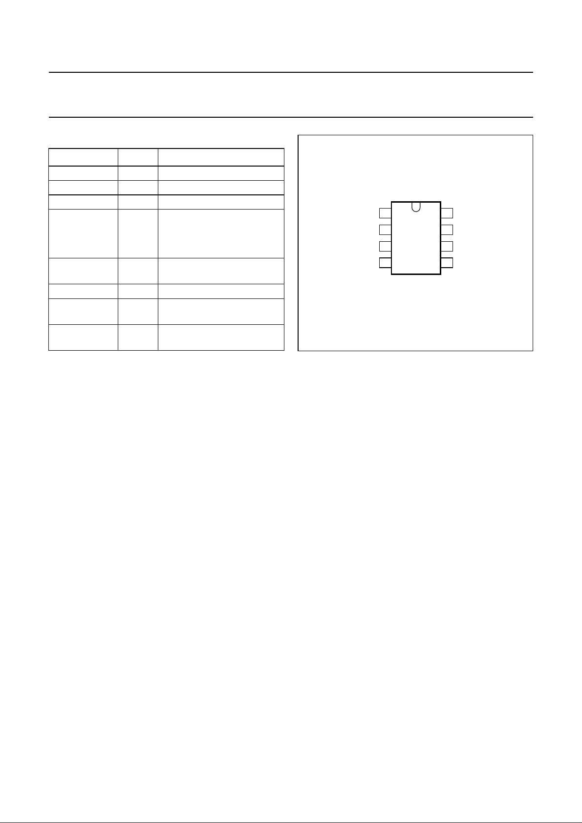
3 ORDERING INFORMATION
TYPE
NUMBER
TEA1541P DIP8 plastic dual-in-line package; 8 leads (300 mil) SOT97-1
2003 Aug 11 3
NAME DESCRIPTION VERSION
PACKAGE
Page 4
Philips Semiconductors Product specification
SMPS control IC with
synchronization function
handbook, full pagewidth
V
mains
Sync
pulses
C
VCC
1
2
TEA1541P
3
4
R
DEM
TEA1541
C
VIN
8
n.c.
7
6
5
MDB082
Fig.1 Basic application.
2003 Aug 11 4
Page 5
Philips Semiconductors Product specification
SMPS control IC with
synchronization function
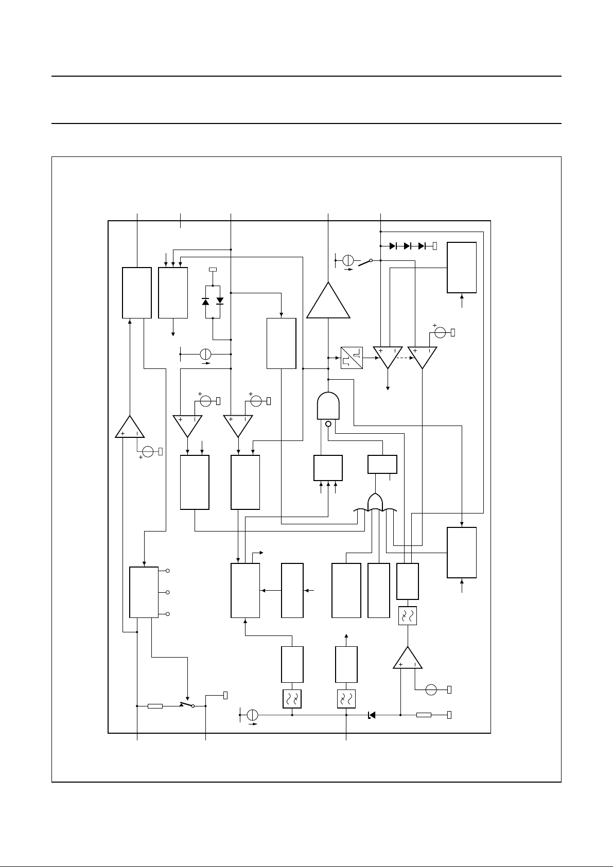
4 BLOCK DIAGRAM
(internal
control)
PRIMARY
CURRENT
PCS
HVS
7
SIMULATION
VIN
8
SOURCE
CURRENT
START-UP
Clamp
DEM
I
−50 mV
4
DEM
100 mV
PROTECTION
OVERVOLTAGE
DRIVER
6
DRIVER
TEA1541
sense
I
5
MDB083
SS
I
soft
start
S2
PROTECTION
OVERPOWER
(frequency
880 mV
information)
LEB
blank
short-
circuit
winding
OCP
700 mV
SUPPLY
MANAGEMENT
1
mains ok
DEM
SHORT-CIRCUIT
UVLO start
supply
internal
S1
OCP
PROTECTION
2
MODE
PROTECTION
CONTINUOUS
(frequency
VOLTAGE
OSCILLATOR
CONTROLLED
CTRL
I
information)
CONTROL
FREQUENCY
SYNC.
DETECTOR
LOGIC
PCS
control)
(internal
OCP
OVER-
PROTECTION
TEMPERATURE
control)
(internal
SAMPLE-
AND-HOLD
3
Q
S
R
UVLO
RESET
POWER-ON
3.5 V
BURST
CONTROL
burst
detect
ON-TIME
MAXIMUM
PROTECTION
(frequency
information)
TEA1541
handbook, full pagewidth
Fig.2 Block diagram.
This text is here in white to force landscape pages to be rotated correctly when browsing through the pdf in the Acrobat reader.This text is here in
_white to force landscape pages to be rotated correctly when browsing through the pdf in the Acrobat reader.This text is here inThis text is here in
white to force landscape pages to be rotated correctly when browsing through the pdf in the Acrobat reader. white to force landscape pages to be ...
2003 Aug 11 5
CC
V
GND
CTRL
Page 6
Philips Semiconductors Product specification
SMPS control IC with
synchronization function
5 PINNING
SYMBOL PIN DESCRIPTION
V
CC
GND 2 ground
CTRL 3 control input
DEM 4 input from auxiliary winding
I
sense
DRIVER 6 gate driver output
HVS 7 high voltage safety spacer,
VIN 8 input for start-up current and
6 FUNCTIONAL DESCRIPTION
The TEA1541 is intended as the controller for a compact
flyback converter for CRT monitor applications. The IC is
situated on the primary side of the output transformer.
Output power is determined by the current in the primary
winding. The voltage across an auxiliary winding in the
transformer is converted to a current by resistor R
used by theIC to derive the current in theprimary winding.
This winding is also used for continuous mode protection,
overvoltage protection, and to power the IC after start-up.
The IC can operate in either synchronized or
unsynchronized mode. In synchronized mode, the IC
synchronizes the converter switching frequency to the
monitor line frequency to prevent interference.
Line synchronizing pulses are applied to pin CTRL.
1 supply voltage
for demagnetization timing,
OVP and overpower
protection (OPP)
5 programmablecurrent sense
input
not connected
mains voltage recognition
and
DEM
TEA1541
handbook, halfpage
The IC has an internal frequency divider which allows it to
operate in synchronized mode at a lower frequency than
the synchronizing pulses supplied to pin CTRL by the
application. The limited frequency range allows an
economical design of the transformer.
In unsynchronized mode, when the power that is drawn
from the converter decreases, the converter switching
frequency also decreases. At very low power (standby)
levels, the frequency of the VCO decreases from 25 kHz
to the minimumvalue of approximately 6 kHz as shown by
the slope of Fig.4. In a typical application it is possible to
obtain an input power of less than 3 W with an output
power of 100 mW.
1
V
CC
2
GND
CTRL
DEM
TEA1541P
3
4
MDB084
Fig.3 Pin configuration.
8
7
6
5
VIN
HVS
DRIVER
I
sense
Each operating cycle of the convertercomprises a primary
stroke followed by a secondary stroke. During the primary
stroke, current flows in the primary winding.
The secondary stroke transfers the energy stored in the
transformer core to the secondary winding. In either
synchronized or unsynchronized mode, the primary stroke
only starts at the end of the secondary stroke when the
transformer is demagnetized to ensure zero switching
primary current. If no synchronizing pulses are present
(unsynchronized mode), the IC will operate at its minimum
switching frequency.
2003 Aug 11 6
Page 7

Philips Semiconductors Product specification
SMPS control IC with
synchronization function
f
handbook, halfpage
(kHz)
50
synchronized operation
25
6
VCO
variable
unsynchronized operation
VCO
fixed
Fig.4 Multi mode operation.
P(W)
MDB085
handbook, halfpage
M-level
V
CC(start)
V
CC(trip)(VIN)
I
VIN(max)
I
VIN(min)
V
I
VIN
CC
VIN
I
CC
TEA1541
6.1 Start-up, mains voltage-dependent
operation-enabling level and undervoltage
lock-out
Initially, the IC is supplied by the rectified mains voltage at
pin VIN. When the voltage at pin VCC is below the V
voltage for VIN current trip level V
current drawn from pin VIN, (I
I
. When VCC rises to the V
VIN(min)
VIN
CC(trip)(VIN)
) is at the low value
CC(trip)(VIN)
, the supply
level, the
current at pin VIN changes to the high value I
VIN(max)
CC
.
When the voltage at pin VIN is below the mains
voltage-dependent operation-enabling level (M-level), the
IC supply capacitor C
is charged by the internal
VCC
start-up current source to approximately 5 V. When the
voltage at pin VIN exceeds the M-level, the start-up
current source continuesto charge C
(switch S1 open;
VCC
see Fig.2).
When VCCreaches the start-up voltage level V
CC(start)
, the
ICswitches to high efficiency(green function) operation by
no longer drawing current from pin VIN (see Fig.5).
At V
the IC activates the external MOSFET. When
CC(start)
the voltage across the auxiliary winding rises above the
voltage across C
, the IC supply current will be supplied
VCC
by the auxiliary winding via pin VCC.
If the voltage on pin VCCfalls below the VCCundervoltage
lock-out level V
CC(UVLO)
, the IC stops switching and enters
a safe restart mode in which current to the IC is supplied
by the rectified mains voltage via pin VIN, and C
VCC
is
re-charged by the internal start-up current source to
V
CC(start)
.
MDB087
Fig.5 Start-up sequence.
Inhibiting the auxiliary supply by external means causes
the converter to operate in a stable, well-defined burst
mode. This is a burst standby mode that is less efficient
than the normal burst standby mode described in
section 6.12.
Ifthe voltage at pin VINfallsbelow the mains undervoltage
lock-out level M
, a safe restart mode is activated, and
UVLO
the IC stops switching.
During normal operation (non-burst standby mode), the
duty cycle of the IC, and thus the output power of the
supply, is regulated by a control voltage at pin CTRL.
If pin VCC is connected to ground, the IC switches to low
power standby operation and the start-up current drawn
via pin VIN reduces to 400 µA (typical). When the voltage
on pin VCC rises above 700 mV (typical), the start-up
current increases to 1 mA (typical).
6.2 Supply management
All internal reference voltages are derived from a
temperature compensated, on-chip bandgap.
2003 Aug 11 7
Page 8

Philips Semiconductors Product specification
SMPS control IC with
synchronization function
6.3 Primary current regulation
The IC uses current mode control for its good line
regulation behaviour. The primary current is sensed
indirectly via the voltage at pin DEM.
The ‘on-time’ of the external MOSFET is controlled by the
voltage on pin CTRL which is compared with the internal
simulated primary current information. For pin CTRL
voltages (V
calculated by the equation:
t
α
on
PCS
where:
• t
: the on-time
on
•α
: an internal constant which is approximately 0.9.
PCS
• V
• I
: the voltage on pin CTRL
CTRL
:thecurrent drawn from pin DEM during theprimary
DEM
cycle.
) between 1 and 1.6 V, the on-time is
CTRL
1.6 V
–
× ns[]=
CTRL
------------------------------I
DEM
TEA1541
handbook, halfpage
Fig.6 Switching frequency as a function of the
f
(kHz)
f
smps(max)
f
osc
f
sync
(min)
synchronizing frequency.
f
sync
(max)
2 × f
(max)
sync
f
(kHz)
MDB086
6.4 Oscillator
In synchronized mode, the switching frequency of the
SMPS f
is controlled by the synchronizing pulses f
smps
sync
at pin CTRL. Synchronized mode prevents noise
disturbance on the CRT monitor screen. Synchronizing
pulseswhose frequency isoutside of the f
osc
andf
smps(max)
window of 26 to 54 kHz are divided by an internal
frequency divider. A small frequency hysteresis exists to
ensure a stable frequency switch-over. In unsynchronized
mode, the system runs at f
(26 kHz). In unsynchronized
osc
mode, at verylow power (standby)levels, the frequency of
theVCO and consequentlythe SMPS switching frequency
is reduced linearly to its low value of approximately 6 kHz
(see Figs 4 and 6).
6.5 Demagnetization
The system always operates in discontinuous conduction
modeto ensure demagnetizationof the output transformer
core.A primary cycleonlystarts when thesecondary cycle
has ended.
Pin DEM protects against an output short-circuit on a
cycle-by-cycle basis, by immediately lowering the
switching frequency to give a longer off-time and a lower
operating power.
Demagnetization detection is suppressed automatically at
the start of each secondary cycle for a period t
suppr
.
Suppressionofdemagnetizationdetectionisnecessaryfor
applications where the transformer has a large leakage
inductance, at low output voltages and at start-up.
If, due to a fault condition, pin DEM is left open circuit,
operation of the flyback converter supply immediately
stops, and restartswhen the faultsituation is removedand
pin DEM is reconnected.
If, during start-up, a fault condition causes pin DEM to be
shorted to ground, operation of the flyback converter
supply stops after the first cycle, and the IC then begins a
restart cycle. This situation continues until the short-circuit
is removed. Short-circuit protection is also active at full
power to ensure limitation of peak current.
2003 Aug 11 8
Page 9

Philips Semiconductors Product specification
SMPS control IC with
synchronization function
6.6 Minimum and maximum ‘on-time’
The minimum on-time of the converter is notlimited by the
leading edge blanking time, and therefore can be zero.
The IC limits the maximum on-time to
where f
is the converter switching frequency in either
smps
synchronized or unsynchronized mode. If the system
requires a longer on-time, a fault condition is assumed, for
example, if C
is removed, the IC willstop switching and
VIN
enter the safe restart mode.
6.7 Overvoltage protection
The TEA1541 allows OVP to be set accurately.
The flyback converter output voltage is accurately
represented by the voltage across the auxiliary winding.
The auxiliary winding voltage is monitored by the current
flowinginto pin DEM during the demagnetizingcycleof the
transformer. The inevitable voltage spikes at pin DEM are
reduced using an internal filter.
1
------------f
smps
TEA1541
prematurely due to the false sensing of an overcurrent
condition caused by current spikes produced by the
discharge of primary-side snubber and parasitic
capacitances.
The OCP level is adjusted proportionally to the switching
frequency such that the product of (I
stays constant. This arrangement also implements OPP,
ensuringthatthemaximum output power is independentof
theswitchingfrequency, otherwise the output powerwould
increase in direct proportion to the switching frequency.
6.9 Soft start
The soft start function allows the transformer peak current
to slowly increase at every start-up and restart, to prevent
transformer rattle.
The soft start function requires a resistor RSS and
capacitor CSSto be connected between pin I
sense resistor R
(see Fig.7). CSS is charged by an
sense
internal current source ISSto V = ISS× RSS, to a maximum
of approximately 0.5 V.
)2× frequency
peak
sense
and the
If the output voltage causes the current into pin DEM to
exceed the OVP level l
OVP(DEM)
, the OVP circuit turns off
the power MOSFET. The controller then waits until the
V
CC(UVLO)
condition is reached. This is followed by a safe
restart cycle, before switching recommences.
This process is repeated until the OVP condition ends.
Theoutputvoltage at which OVPactivates,V
the value of resistor, R
N
V
o(ovp)
----------N
aux
s
I
, (see Fig.8) using the equation:
DEM
R
OVP DEM()
+×()×=
DEMVclamp DEM()pos()
o(ovp)
issetby
where N is the number of turns on the transformer
windings; V
clamp(DEM)(pos)
pin DEM; reference current I
is the positive clamp voltage on
OVP(DEM)
is set internally.
6.8 Overcurrent protection and overpower
protection
The current in the transformer primary is measured
accurately by the internal cycle-by-cycle source current
limit circuit using the external sense resistor R
sense
.
The accuracy of the current limit circuit allows the
transformer core to have a minimum specification for the
output power required. The OCP circuit limits the ‘sense’
voltage to an internal level, and is activated after the
leading edge blanking period, t
generated by the
leb
Leading Edge Blanking circuit (LEB shown in Fig.2).
Leading edge blanking is required to inhibit OCP for a
short period when the power MOSFET turns on.
This ensures that the MOSFET is not turned off
handbook, halfpage
I
SS
0.5 V
start-up
V
ocp
5
I
sense
R
SS
C
SS
R
sense
MBL503
Fig.7 Soft start.
The rate at which the primary current increases can be
adjustedby changing thevalues of RSSandCSStochange
the circuit time constant:
τ RSSCSS×=
The maximum primary current is calculated by the
equation:
I
primary max()
V
sense max()
=
------------------------------------------------------------------
ISSRSS×()–
R
sense
2003 Aug 11 9
Page 10

Philips Semiconductors Product specification
SMPS control IC with
synchronization function
where V
sense(max)
ISS flows when the voltage on pin I
approximately 0.5 V. If this voltage exceeds 0.5 V, the
soft-start current source starts to limit ISS and completely
switches ISS off at V
Note that ISS is derived from the internal current source
supplying charging current to pin VCC. During soft-start,
the charging current to pin VCC will be reduced by up to
60 µA depending on the value of RSS.
6.10 Winding short-circuit protection
Thewindingshort-circuitprotectioncircuit is activated after
the leading edge blanking period. A short-circuit in the
transformer winding is detected when the voltage at
pin I
voltage V
exceeds the winding short-circuit protection
sense
swp
converter supply will stop switching. When the voltage at
pin VCC falls below V
mode, and capacitor C
start-up current source supplied from pin VIN until the
flyback converter supply restarts at V
detection and restart cycle will be repeated until the
short-circuit is removed. The winding short-circuit
protection circuit also provides protection if a diode in the
transformer secondary circuit goes short-circuit.
is the maximum source voltage for OCP.
is less than
sense
.
CC(start)
. When a short-circuit is detected, the flyback
CC(UVLO)
, the IC enters safe restart
will recharge via the internal
VCC
. The fault
CC(start)
TEA1541
period that is longer than the burst standby mode blanking
period t
blank(burst)
Duringa burst standbymode cycle, thesoft-start capacitor
CSS, (see Fig.8) is charged to 1.25 V and then discharged
via the soft-start resistor R
0.5 V, a soft-restart is initiated. The frequency of a typical
burst standby mode cycle is approximately:
If, during a burst standby mode cycle, the voltage at
pin V
falls below the trip level voltage V
CC
willbe supplied againfrom pin VIN. IfV
within the burst cycle period due to an external load on
pin V
, a restart cycle begins. If during a burst standby
CC
mode cycle, the voltage on pin V
level voltage V
obtained because the IC is being consistently powered by
the auxiliary winding.
6.13 Driver
The Gate of the external power MOSFET is driven from a
driver circuit having a current sourcing capability of
typically 100 mA, and a current sink capability of typically
500 mA.This permits fastturn-onand turn-off ofthe power
MOSFET for efficient operation.
.
CC(burst)
. When CSS is discharged to
SS
1
--------------------------- -
×
R
SSCSS
CC(burst)
CC(UVLO)
stays above the trip
CC
, the IC
isreached
, a maximum burst efficiency is
6.11 Overtemperature protection
An accurate temperature protection circuit stops the
converter from switching if the IC junction temperature
exceeds the maximum temperature protection level
T
prot(max)
V
CC(UVLO)
C
VCC
. When the voltage at pin VCC falls below
, the IC enters safe restart mode, and capacitor
will recharge to V
via the internal start-up
CC(start)
current source derived from pin VIN. If the temperature is
still too high, the voltage at pin VCC will fall again to
V
CC(UVLO)
temperature falls 8 degrees (typical) below T
. This cycle is repeated until the junction
prot(max)
.
6.12 Burst standby mode
Pin CTRL and pin I
are also used to implement the
sense
burst standby mode feature. In burst standby mode, the
converter consumes lessthan 1 W (typical)of input power
at a maximum output power of 100 mW. This power is
sufficient to supply a low power device such as a
microcontroller. Burst standby mode is entered when a
current larger than the burst standby mode active current
I
is forced into pin CTRL, via the opto-coupler, for a
burst
A low driver source current has been chosen in order to
limit the ∆V/∆t at switch-on. Thisreduces Electro Magnetic
Interference (EMI) and also limits the voltage spikes
across the current sense resistor R
sense
.
2003 Aug 11 10
Page 11

Philips Semiconductors Product specification
SMPS control IC with
TEA1541
synchronization function
7 LIMITING VALUES
In accordance with the Absolute Maximum Rating System (IEC 60134). All voltages are measured with respect to
ground (pin 2); positive currents flow into the chip; pin 1 is not allowed to be current driven. The voltage ratings are valid
provided other ratings are not being violated; current ratings are valid provided the maximum power rating is not
violated.
SYMBOL PARAMETER CONDITIONS MIN. MAX. UNIT
V
CC
V
CTRL
V
DEM
V
sense
V
VIN
I
CTRL
I
DEM
I
sense
I
DRIVER
I
VIN
P
tot
T
stg
T
j
V
esd
voltage on pin V
CC
voltage on pin CTRL −0.4 +5V
voltage on pin DEM current limited −0.4 − V
voltage on pin I
sense
voltage on pin VIN −0.4 +550 V
current on pin CTRL δ < 10% − 50 mA
current on pin DEM −250 +250 µA
current on pin I
sense
current on pin DRIVER δ < 10% −0.8 +2A
current pin VIN −+5mA
total power dissipation T
storage temperature −55 +150 °C
junction temperature −20 +145 °C
electrostatic discharge;
human body model; note 1 pins 1 to 6 (class II) − 2000 V
machine model; note 2 − 200 V
continuous −0.4 +40 V
current limited −0.4 − V
−1 +10 mA
<70°C − 0.75 W
amb
pin 8 (Vin) (class I) − 1250 V
Notes
1. Equivalent to discharging a 100 pF capacitor through a 1.5 kΩ series resistor.
2. Equivalent to discharging a 200 pF capacitor through a 0.75 µH coil and a 10 Ω resistor.
8 THERMAL CHARACTERISTICS
SYMBOL PARAMETER CONDITIONS VALUE UNIT
R
th(j-a)
thermal resistance from junction to ambient in free air 100 K/W
9 QUALITY SPECIFICATION
In accordance with
“SNW-FQ-611 part D”
.
2003 Aug 11 11
Page 12

Philips Semiconductors Product specification
SMPS control IC with
TEA1541
synchronization function
10 CHARACTERISTICS
T
=25°C; VCC= 15 V; all voltages are measured with respect to ground (pin 2); currents are positive when flowing
amb
into the IC.
SYMBOL PARAMETER CONDITIONS MIN. TYP. MAX. UNIT
Start-up current source (pin VIN)
I
VIN(min)
V
CC(VIN)trip
I
VIN(max)
I
VIN
V
bd
M-level mains-dependentoperation-enabling
M
UVLO
VCC management (pin VCC)
minimum supply current drawn from
pin VIN
supply voltage for pin VIN current trip
VCC<V
V
V
CC(trip)(VIN)
> 100 V
VIN
> 100 V 0.5 0.75 1.0 V
VIN
,
300 400 500 µA
level
maximum supply current drawn from
pin VIN
supply current drawn from pin VIN after start-up;
VCC=10V;
V
> 100 V
VIN
V
CC>VCC(start)
V
> 100 V
VIN
1.25 1.6 1.95 mA
− 100 300 µA
;
breakdown voltage 550 −−V
33 37 40 V
level
mains undervoltage lock-out level 25 28.5 33 V
V
CC(start)
V
CC(UVLO)
V
CC(hys)
I
CC(h)
I
CC(l)
I
CC(restart)
I
CC(oper)
start-up voltage 10.8 11.4 12 V
undervoltage lock-out 8.5 9.0 9.5 V
hysteresis voltage V
charging current (high) V
charging current (low) V
restart current V
supply current under normal
operation
Primary current simulation
α
PCS
primary current simulation factor − 0.9 − A.s/V
Demagnetization management (pin DEM)
V
th(DEM)
demagnetization comparator
threshold voltage
I
prot(DEM)
V
clamp(DEM)(neg)
V
clamp(DEM)(pos)
t
suppr
demagnetization current −50 −−10 nA
negative clamp voltage I
positive clamp voltage I
suppression time of transformer
ringing at start of secondary stroke
V
sc(prot)(DEM)
short-circuit protection voltage −90 −50 −10 mV
CC(start)
VIN
VCC<V
VIN
V
CC(trip)(VIN)<VCC
<V
VIN
<VCC<V
− V
> 100 V;
CC(trip)(VIN)
> 100 V;
CC(UVLO)
> 100 V;V
CC(start)
CC(UVLO)
CC(UVLO)
2.1 2.4 2.7 V
−−0.25 − mA
−1.6 −1.2 −0.75 mA
−1.25 −1.0 −0.75 mA
no load on pin DRIVER − 1.6 − mA
70 100 130 mV
= −150 µA −0.5 −0.25 −0.05 V
(DEM)
= 250 µA 0.55 0.7 0.85 V
(DEM)
1.1 1.5 1.9 µs
2003 Aug 11 12
Page 13

Philips Semiconductors Product specification
SMPS control IC with
TEA1541
synchronization function
SYMBOL PARAMETER CONDITIONS MIN. TYP. MAX. UNIT
Pulse width modulator
t
on(min)
t
on(max)
Oscillator
f
osc(min)
f
osc
f
smps(max)
f
smps(hys)
V
vco(start)
V
vco(max)
Duty cycle control (pin CTRL)
V
CTRL(min)
V
CTRL(max)
I
prot(CTRL)
Burst standby mode (pin CTRL)
V
th(burst)(on)
I
burst
t
blank(burst)
V
ch(sense)(burst)
V
dis(sense)(burst)
I
ch(sense)(burst)
V
CC(burst)
I
CC(burst)
Synchronization (pin CTRL)
V
sync
∆V/∆t
sync
minimum on-time − 0 −
maximum on-time latched − 1/f
minimum oscillator frequency V
oscillator frequency V
> 1.5 V; no sync − 6 − kHz
CTRL
< 1.5 V; no sync;
CTRL
24 26 28 kHz
smps
− s
note 2
maximum SMPS switching
sync. on; note 3 − 54 − kHz
frequency before frequency division
frequency hysteresis for division sync. on − 4 − kHz
voltage on pin CTRL where
sync off 1.38 1.46 1.54 V
frequency reduction starts
peak voltage on pin CTRL where
frequency is equal to f
osc(min)
minimum voltage on pin CTRL for
sync off − 1.58 − V
− 1.0 − V
maximum duty cycle
maximum voltage on pin CTRL for
− 1.6 − V
minimum duty cycle
current on pin CTRL −0.6 −0.8 −1.0 µA
burst standby mode active threshold
I
=4mA − 3.6 − V
burst
voltage
burst standby mode active current 4 7 11 mA
burst standby mode blanking time 25 32 40 µs
charge voltage on pin I
sense
in burst
− 1.25 − V
standby mode
discharge voltage level on pin I
sense
− 0.5 − V
in burst standby mode
charging current into pin I
sense
in
− 100 −µA
burst standby mode
supply voltage trip level for supply
− 11.2 − V
from pin VIN during burst standby
mode
supply current during burst standby
− 600 −µA
mode
synchronization recognition voltage 0.37 0.52 0.65 V
synchronization recognition − 0.5
(1)
− V/µs
2003 Aug 11 13
Page 14

Philips Semiconductors Product specification
SMPS control IC with
TEA1541
synchronization function
SYMBOL PARAMETER CONDITIONS MIN. TYP. MAX. UNIT
Overcurrent and winding short-circuit protection (pin I
V
sense(max)
t
PD
V
swp
maximum source voltage for OCP f
propagation delay from detecting
V
sense(max)
to switch-off
winding short-circuit protection
voltage
t
leb
blanking time forcurrent and winding
short-circuit protection
I
ss
V
ss(max)
soft start current V
soft start maximum sense voltage 0.45 0.50 0.55 V
Overvoltage protection (pin DEM)
I
OVP(DEM)
OVP trigger current see Section
Driver (pin DRIVER)
I
source
I
sink
V
o(driver)(max)
source current capability of driver VCC= 9.5 V;
sink current capability of driver VCC= 9.5 V;
maximum output voltage of driver VCC>12V − 11.5 12 V
Temperature protection
T
prot(max)
maximum temperature protection
level
T
prot(hys)
hysteresis for the temperature
protection level
)
sense
smps(min)
;
0.48 0.52 0.56 V
∆V/∆t = 0.1 V/µs
f
smps(max)
;
0.33 0.37 0.41 V
∆V/∆t = 0.1 V/µs
∆V/∆t = 0.5 V/µs − 140 185 ns
∆V/∆t = 0.5 V/µs 0.83 0.88 0.96 V
320 380 480 ns
< 0.5 V 45 60 75 µA
sense
54 60 66 µA
“Overvoltage protection”
−−100 −75 mA
V
DRIVER
=5V
− 500 − mA
V
V
V
DRIVER
= 9.5 V;
CC
DRIVER
=5V
400 700 − mA
= 9.5 V
130 140 150 °C
− 8 −°C
Notes
1. Guaranteed by design.
2. This is also the minimum SMPS switching frequency in synchronized mode.
3. This is also the maximum oscillator frequency in synchronized mode.
2003 Aug 11 14
Page 15

Philips Semiconductors Product specification
SMPS control IC with
synchronization function
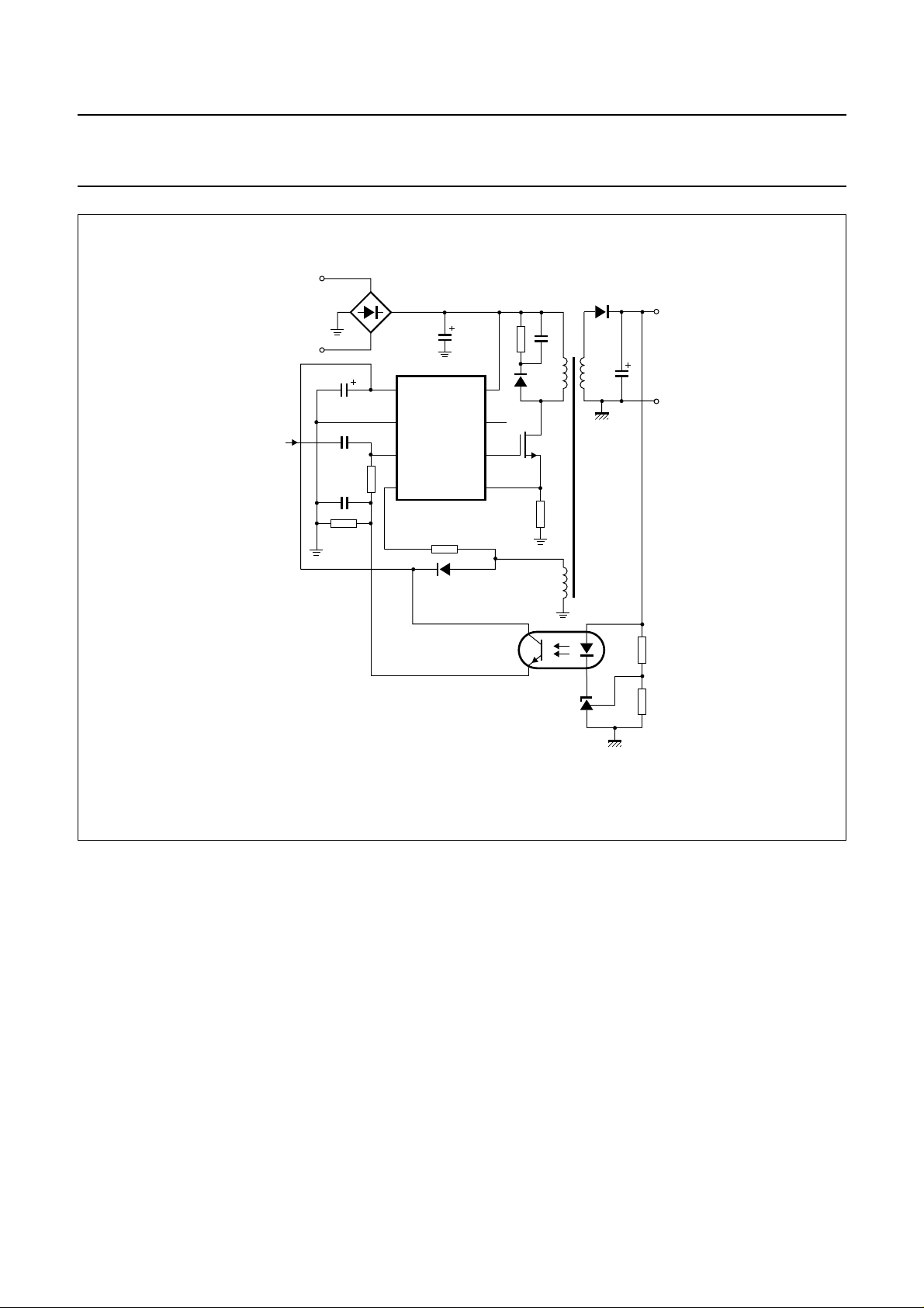
11 APPLICATION INFORMATION
Atypical flyback converter that usestheTEA1541 consists
of an input filter, a transformer with a third (auxiliary)
winding, and an output stage with a feedback circuit.
CapacitorC
voltage from the rectified high voltage (AC) mains during
start-up, or from the auxiliary winding during operation.
Resistor R
at pin I
sense
primary peak current. Resistor RSS and capacitor C
enable soft start and burst standby mode operation.
handbook, full pagewidth
Sync
connectedto pin VCCbuffersthe IC supply
VCC
converts the primary current into a voltage
sense
. The resistor value defines the maximum
V
mains
C
C
R
SYNC
C
R
VCC
SYNC
REG
REG
V
CC
GND
CTRL
DEM
1
2
3
4
TEA1541P
SS
C
8
7
6
5
VIN
VIN
HV
DRIVER
I
TEA1541
A resistor and a series diode can be placed inparallel with
resistor R
and out of the IC, allowing the valuesof theOVP leveland
primary current simulation to be defined independently.
More details are available in
R
SNUB
D
SNUB
R
C
R
SS
SS
DEM
sense
to control the amount of current flowing into,
DEM
Application note AN10205
D
OUT
C
SNUB
OUTPUT
power
MOSFET
R
sense
C
OUT
.
MDB081
Fig.8 Flyback configuration with synchronization and soft start.
2003 Aug 11 15
D
VCC
OPTO
R
REG1
R
REG2
Page 16

Philips Semiconductors Product specification
SMPS control IC with
synchronization function
12 PACKAGE OUTLINE
DIP8: plastic dual in-line package; 8 leads (300 mil)
D
seating plane
A
L
Z
e
b
8
1
w M
b
1
b
2
5
TEA1541
SOT97-1
M
E
A
2
A
c
(e )
1
M
H
pin 1 index
E
1
DIMENSIONS (inch dimensions are derived from the original mm dimensions)
A
A
A
UNIT
max.
mm
inches
Note
1. Plastic or metal protrusions of 0.25 mm (0.01 inch) maximum per side are not included.
OUTLINE
VERSION
SOT97-1
12
min.
max.
050G01 MO-001 SC-504-8
b
1.73
1.14
0.068
0.021
0.045
0.015
IEC JEDEC JEITA
b
1
0.53
0.38
4
0 5 10 mm
scale
b
2
0.36
1.07
0.23
0.89
0.014
0.042
0.009
0.035
REFERENCES
(1) (1)
cD E e M
9.8
6.48
9.2
6.20
0.39
0.26
0.36
0.24
L
e
1
M
3.60
8.25
3.05
7.80
0.14
0.32
0.12
0.31
EUROPEAN
PROJECTION
E
10.0
8.3
0.39
0.33
H
0.2542.54 7.62
ISSUE DATE
w
0.010.1 0.3
99-12-27
03-02-13
max.
1.154.2 0.51 3.2
0.0450.17 0.02 0.13
(1)
Z
2003 Aug 11 16
Page 17

Philips Semiconductors Product specification
SMPS control IC with
synchronization function
13 SOLDERING
13.1 Introduction to soldering through-hole mount
packages
This text gives a brief insight to wave, dip and manual
soldering.A more in-depth accountofsoldering ICs can be
found in our
Packages”
Wave soldering is the preferred method for mounting of
through-hole mount IC packages on a printed-circuit
board.
13.2 Soldering by dipping or by solder wave
Driven by legislation and environmental forces the
worldwide use of lead-free solder pastes is increasing.
Typical dwell time of the leads in the wave ranges from
3 to 4 seconds at 250 °C or 265 °C, depending on solder
material applied, SnPb or Pb-free respectively.
Thetotalcontact time of successive solderwavesmustnot
exceed 5 seconds.
“Data Handbook IC26; Integrated Circuit
(document order number 9398 652 90011).
TEA1541
The device may be mounted up to the seating plane, but
the temperature of the plastic body must not exceed the
specified maximum storage temperature (T
printed-circuit board has been pre-heated, forced cooling
may be necessary immediately after soldering to keep the
temperature within the permissible limit.
13.3 Manual soldering
Apply the soldering iron (24 V or less) to the lead(s) of the
package, either below the seating plane or not more than
2 mm above it. If the temperature of the soldering iron bit
is less than 300 °C it may remain in contact for up to
10 seconds. If the bit temperature is between
300 and 400 °C, contact may be up to 5 seconds.
stg(max)
). If the
13.4 Suitability of through-hole mount IC packages for dipping and wave soldering methods
PACKAGE
DBS, DIP, HDIP, SDIP, SIL suitable suitable
(2)
PMFP
Notes
1. For SDIP packages, the longitudinal axis must be parallel to the transport direction of the printed-circuit board.
2. For PMFP packages hot bar soldering or manual soldering is suitable.
− not suitable
DIPPING WAVE
SOLDERING METHOD
(1)
2003 Aug 11 17
Page 18

Philips Semiconductors Product specification
SMPS control IC with
TEA1541
synchronization function
14 DATA SHEET STATUS
LEVEL
I Objective data Development This data sheet contains data from the objective specification for product
II Preliminary data Qualification This data sheet contains data from the preliminary specification.
III Product data Production This data sheet contains data from the product specification. Philips
Notes
1. Please consult the most recently issued data sheet before initiating or completing a design.
2. The product status of the device(s) described in this data sheet may have changed since this data sheet was
3. For data sheets describing multiple type numbers,the highest-levelproduct statusdetermines thedata sheet status.
DATA SHEET
STATUS
published. The latest information is available on the Internet at URL http://www.semiconductors.philips.com.
(1)
PRODUCT
STATUS
(2)(3)
development. Philips Semiconductors reserves the right to change the
specification in any manner without notice.
Supplementary data will be published at a later date. Philips
Semiconductors reserves the right to change the specification without
notice, in order to improve the design and supply the best possible
product.
Semiconductors reserves the right to make changes at any time in order
to improve the design, manufacturing and supply. Relevant changes will
be communicated via a Customer Product/Process Change Notification
(CPCN).
DEFINITION
15 DEFINITIONS
Short-form specification The data in a short-form
specification is extracted from a full data sheet with the
same type number and title. For detailed information see
the relevant data sheet or data handbook.
Limiting values definition Limiting values given are in
accordance with the Absolute Maximum Rating System
(IEC 60134). Stress above one or more of the limiting
values may cause permanent damage to the device.
These are stress ratings only and operation of the device
atthese or at anyotherconditionsabove those given inthe
Characteristics sections of the specification is not implied.
Exposure to limiting values for extended periods may
affect device reliability.
Application information Applications that are
described herein for any of these products are for
illustrative purposes only. Philips Semiconductors make
norepresentationorwarranty that such applications willbe
suitable for the specified use without further testing or
modification.
16 DISCLAIMERS
Life support applications These products are not
designed for use in life support appliances, devices, or
systems where malfunction of these products can
reasonably be expected to result inpersonal injury. Philips
Semiconductorscustomersusingor selling these products
for use in such applications do so at their own risk and
agree to fully indemnify Philips Semiconductors for any
damages resulting from such application.
Right to make changes Philips Semiconductors
reserves the right to make changes in the products including circuits, standard cells, and/or software described or contained herein in order to improve design
and/or performance. Whenthe product is in full production
(status ‘Production’), relevant changes will be
communicated via a Customer Product/Process Change
Notification (CPCN). Philips Semiconductors assumes no
responsibility or liability for the use of any of these
products, conveys no licence or title under any patent,
copyright, or mask work right to these products, and
makes no representations or warranties that these
products are free from patent, copyright, or mask work
right infringement, unless otherwise specified.
2003 Aug 11 18
Page 19

Philips Semiconductors – a w orldwide compan y
Contact information
For additional information please visit http://www.semiconductors.philips.com. Fax: +31 40 27 24825
For sales offices addresses send e-mail to: sales.addresses@www.semiconductors.philips.com.
© Koninklijke Philips Electronics N.V. 2003
All rights are reserved. Reproduction in whole or in part is prohibited without the prior written consent of the copyright owner.
The information presented in this document does not form part of any quotation or contract, is believed to be accurate and reliable and may be changed
without notice. No liability will be accepted by the publisher for any consequence of its use. Publication thereof does not convey nor imply any license
under patent- or other industrial or intellectual property rights.
Printed in The Netherlands 403502/01/pp19 Date of release: 2003 Aug 11 Document order number: 9397 750 10696
SCA75
 Loading...