

Page 1

查询TEA1200TS供应商查询TEA1200TS供应商
INTEGRATED CIRCUITS
DATA SH EET
TEA1200TS
0.95 V starting DC-to-DC converter
with low battery indicator
Product specification 2002 May 14
Page 2

Philips Semiconductors Product specification
0.95 V starting DC-to-DC converter
with low battery indicator
FEATURES
• Complete DC-to-DC converter circuit and battery low
detector
• Configurablefor1, 2 or 3-cellNickel-Cadmium(NiCd)or
Nickel Metal Hydride (NiMH) batteriesand 1 LithiumIon
(Li-Ion) battery
• Guaranteed DC-to-DC converter start-up from 1-cell
NiCd or NiMH battery, even with a load current
• Upconversion or downconversion
• Internal power MOSFETs featuring a low R
approximately 0.1 Ω
• Synchronous rectification for high efficiency
• Soft start
• PWM-only operating option
• Stand-alone low battery detector requires no additional
supply voltage
• Low battery detection level at 0.90 V, externally
adjustable to a higher level
• Adjustable output voltages
• Shut-down function
• Small outline package
• 0.6 µm BICMOS process.
APPLICATIONS
• Cellular phones
• Cordless phones
• Personal Digital Assistants (PDAs)
• Portable audio players
• Pagers
• Mobile equipment.
DSon
of
TEA1200TS
GENERAL DESCRIPTION
The TEA1200TS is a fully integrated battery power unit
including a high-efficiency DC-to-DC converterwhich runs
from a 1-cell NiCd or NiMH battery and a low battery
detector. The circuit can be arranged in several ways to
optimize the application circuit of a power supply system.
Therefore, the DC-to-DC converter can be arranged for
upconversion or downconversion and the low battery
detector can be configured for several types of batteries.
Accurate low battery detection is possible while all other
blocks are switched off.
The DC-to-DC converter features efficient, compact and
dynamic power conversion using a digital control concept
comparable with Pulse Width Modulation (PWM) and
Pulse Frequency Modulation (PFM), integrated CMOS
power switches with a very low R
synchronous rectification.
The device operates at a switching frequency of 600 kHz
which enables the use of external components with
minimum size. The switching frequency can be
synchronized to an external high frequency clock signal.
Optionally, the device can be kept in PWM control mode
only. Deadlock is prevented by an on-chip undervoltage
lockout circuit.
Active current limiting enables efficient conversion in
pulsed-load systems such as Global System for Mobile
communication (GSM) and Digital Enhanced Cordless
Telecommunications (DECT).
The low battery detector has a built-in detection level
which is optimum for a 1-cell NiCd or NiMH battery.
DSon
and fully
ORDERING INFORMATION
TYPE
NUMBER
TEA1200TS SSOP16 plastic shrink small outline package; 16 leads; body width 4.4 mm SOT369-1
2002 May 14 2
NAME DESCRIPTION VERSION
PACKAGE
Page 3

Philips Semiconductors Product specification
0.95 V starting DC-to-DC converter
TEA1200TS
with low battery indicator
QUICK REFERENCE DATA
SYMBOL PARAMETER CONDITIONS MIN. TYP. MAX. UNIT
DC-to-DC converter
UPCONVERSION
V
i(up)
V
o(up)
V
i(start)
V
o(uvlo)
DOWNCONVERSION
V
i(dwn)
V
o(dwn)
CURRENT LEVELS
I
q(DC/DC)
I
shdwn
I
LX(max)
∆I
lim
POWER MOSFETS
R
DSon(N)
R
DSon(P)
EFFICIENCY
η efficiency upconversion see Fig.8; Voup to 3.3 V
TIMING
f
sw
f
i(sync)
t
start
General characteristics
V
ref
input voltage V
output voltage V
− 5.50 V
i(start)
− 5.50 V
o(uvlo)
start-up input voltage IL< 10 mA 0.93 0.96 1.00 V
undervoltage lockout voltage note 1 2.0 2.2 2.4 V
input voltage V
− 5.50 V
o(uvlo)
output voltage 1.30 − 5.50 V
quiescent current at pin
− 110 −µA
UPOUT/DNIN
current in shut-down mode V
maximum continuous current at
LBI1=VI(up)
T
=80°C −−1.0 A
amb
= 1.2 V − 65 −µA
pins LX1 and LX2
current limit deviation I
set to 1.0 A
lim
upconversion −12 − +12 %
downconversion −12 − +12 %
drain-to-sourceon-state resistance
Tj=27°C; IDS= 100 mA − 110 200 mΩ
NFET
drain-to-sourceon-state resistance
Tj=27°C; IDS= 100 mA − 125 250 mΩ
PFET
V
= 1.2 V; IL= 100 mA − 84 − %
i
V
= 2.4 V; IL=10mA − 92 − %
i
switching frequency PWM mode 480 600 720 kHz
synchronization clock input
6 1320MHz
frequency
start-up time − 10 − ms
reference voltage 1.165 1.190 1.215 V
Note
1. The undervoltage lockoutlevel showswide specification limits since it decreases withincreasing temperature.When
the temperature increases, the minimum supply voltage of the digital control part of the IC decreases and therefore
thecorrect operation of this functionis guaranteed overthe whole temperaturerange. The undervoltagelockout level
is measured at pin UPOUT/DNIN.
2002 May 14 3
Page 4
Philips Semiconductors Product specification
0.95 V starting DC-to-DC converter
with low battery indicator
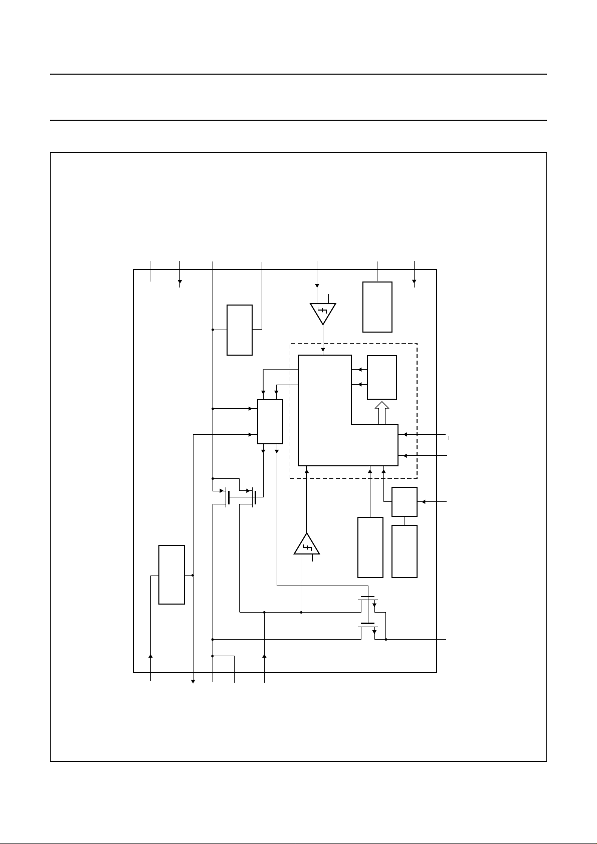
BLOCK DIAGRAM
UPOUT/DNIN
n.c.
3
6
UPOUT/DNIN
4
INTERNAL
SUPPLY
8
GND
TEA1200TS
FB0
12
ref
V
ref
V
11
VOLT AGE
REFERENCE
ref
V
7
MBL409
TEA1200TS
9
TIME
COUNTER
AND
CIRCUIT
START-UP
sense FET
P-type POWER FET
DETECTOR
LOW BATTERY
1
10
5
16
MODE GEARBOX
CONTROL LOGIC
COMPARATOR
CURRENT LIMIT
ref
V
TEMPERATURE
N-type
POWER
PROTECTION
FET
FET
sense
DIGITAL CONTROLLER
GATE
SYNC
13 MHz
OSCILLATOR
SHDWN0
1413 2 15
SYNC/PWM U/D
GND0
Fig.1 Block diagram.
handbook, full pagewidth
This text is here in white to force landscape pages to be rotated correctly when browsing through the pdf in the Acrobat reader.This text is here in
_white to force landscape pages to be rotated correctly when browsing through the pdf in the Acrobat reader.This text is here inThis text is here in
white to force landscape pages to be rotated correctly when browsing through the pdf in the Acrobat reader. white to force landscape pages to be ...
2002 May 14 4
LBI1
LBO
LX1
LX2
ILIM
Page 5

Philips Semiconductors Product specification
0.95 V starting DC-to-DC converter
with low battery indicator
PINNING
SYMBOL PIN DESCRIPTION
LX1 1 inductor connection 1
SHDWN0 2 DC-to-DC converter shut-down
input
UPOUT/DNIN 3 up mode: DC-to-DC converter
output; down mode DC-to-DC
converter input
UPOUT/DNIN 4 up mode: DC-to-DC converter
output; down mode DC-to-DC
converter input
ILIM 5 current limiting resistor
connection
n.c. 6 not connected
V
ref
GND 8 internal supply ground
LBI1 9 low battery detector input 1
LBO 10 low battery detector output
V
ref
FB0 12 DC-to-DC converter feedback
GND0 13 DC-to-DC converter ground
SYNC/PWM 14 synchronization clock input or
U/D 15 conversion mode selection input
LX2 16 inductor connection 2
7 reference voltage input
11 reference voltage input
input
PWM-only selection input
handbook, halfpage
UPOUT/DNIN
UPOUT/DNIN
LX1
1
SHDWN0
ILIM
n.c.
V
ref
GND
2
3
4
TEA1200TS
5
6
7
8
Fig.2 Pin configuration.
TEA1200TS
LX2
16
U/D
15
14
SYNC/PWM
13
GND0
12
FB0
11
V
ref
10
LBO
9
LBI1
MBL419
FUNCTIONAL DESCRIPTION
Control mechanism
The TEA1200TS DC-to-DC converter is able to operate in
the PFM (discontinuous conduction) or PWM (continuous
conduction) operating mode. All switching actions are
completely determined by a digital control circuit which
usesthe output voltage levelasits control input. Thisnovel
digital approach enables the use of a new pulse width and
frequency modulation scheme, which ensures optimum
power efficiency over the complete range of operation of
the converter.
When high output power is requested, the device will
operate in the PWM operating mode. This results in
minimumAC currents in the circuitcomponentsandhence
optimum efficiency, minimum costs and low EMC. In this
operating mode, the output voltage is allowed to vary
between two predefined voltage levels. As long as the
output voltage stays within this so-called window,
switching continues in a fixed pattern.
2002 May 14 5
When the output voltage reaches one of the window
borders, the digital controller immediately reacts by
adjusting the pulse width and inserting a current step in
such a waythat the output voltage stayswithin the window
with higher or lower current capability. This approach
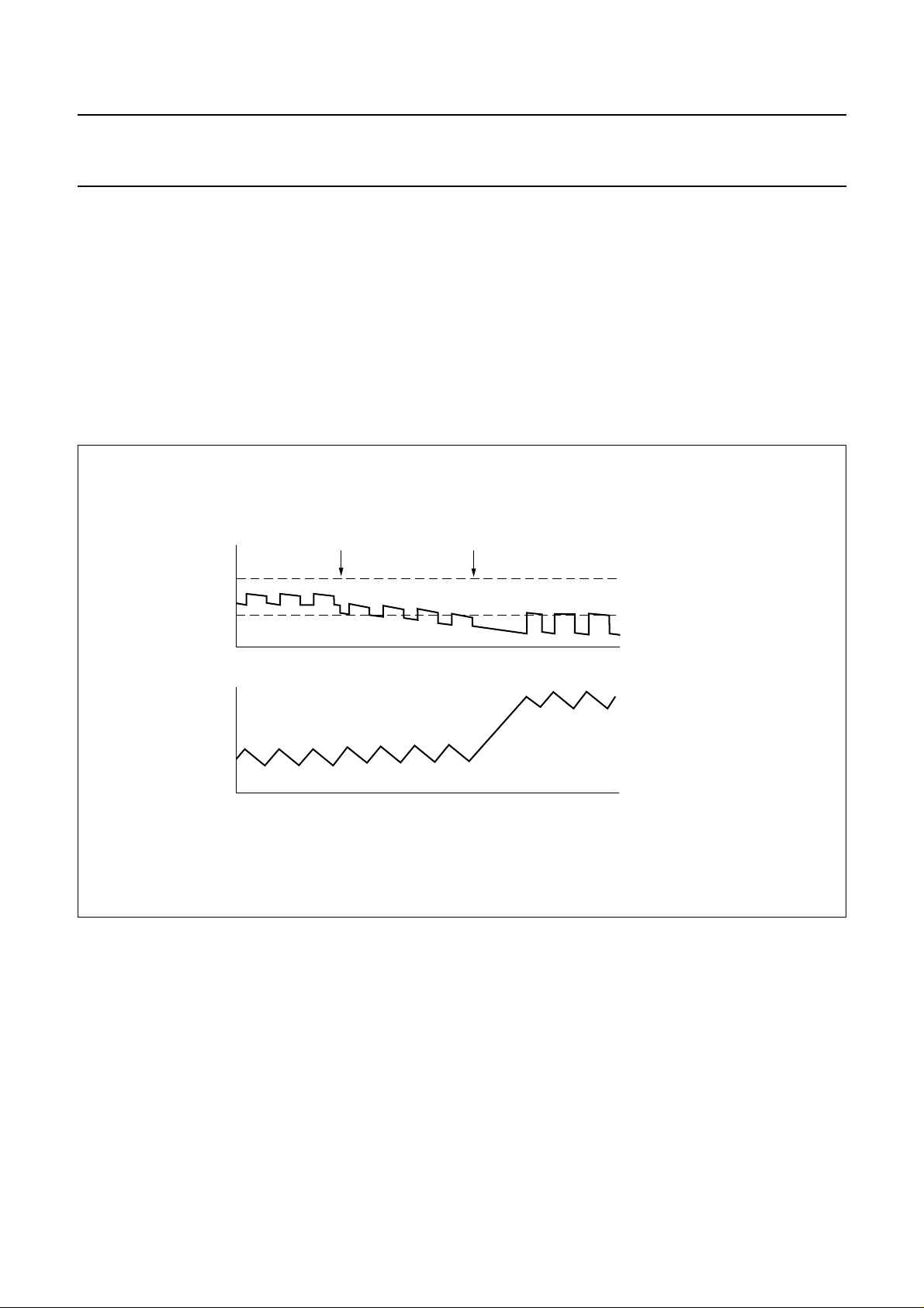
enables very fast reaction to load variations. Figure 3
shows the response of the converter to a sudden load
increase. The upper trace shows the output voltage.
The ripple on top of the DC level is a result of the current
in the output capacitor, which changes in sign twice per
cycle, times the internal Equivalent Series Resistance
(ESR) of the capacitor. After each ramp-down of the
inductor current, i.e. when the ESR effect increases the
output voltage, the converter determines what to do in the
next cycle. As soon as more load current istaken from the
output the output voltage starts to decay.
Page 6
Philips Semiconductors Product specification
0.95 V starting DC-to-DC converter
with low battery indicator
When the output voltage becomes lower than the low limit
of the window, a corrective actionis taken by a ramp-up of
theinductor current duringa much longertime. As aresult,
the DC current level is increasedand normalPWM control
can continue. The output voltage (including ESR effect) is
again within the predefined window.
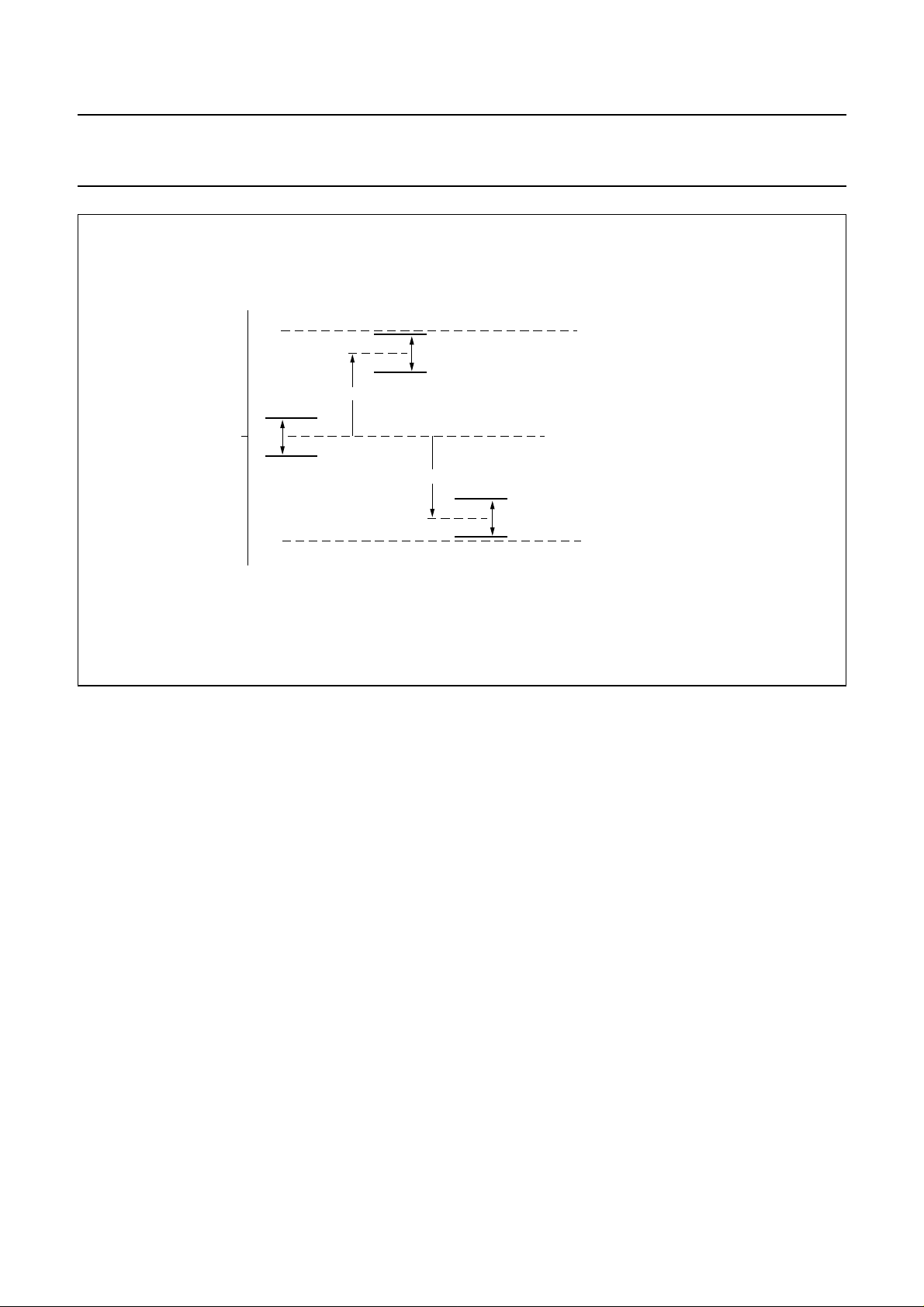
Figure 4 shows the spread of the output voltage window.
The absolute value is mostly dependent on spread, while
the actual window size [V
wdw(high)
affected. For one specific device, the output voltage will
not vary more than 2% (typical value).
handbook, full pagewidth
V
o
− V
wdw(low)
load increase
] is not
start corrective action
TEA1200TS
In low output power situations, the TEA1200TS will switch
over to PFM operating mode. In this mode, regulation
information from an earlier PWM operating mode is used.
This results in optimum inductor peak current levels in the
PFM mode, which are slightly larger than the inductor
ripple current in the PWM mode. As a result, the transition
between PFM and PWM mode is optimum under all
circumstances. In the PFM mode the TEA1200TS
regulates the output voltage to the high window limit as
shown in Fig.3.
high window limit
low window limit
time
I
L
time
MGK925
Fig.3 Response to load increase.
2002 May 14 6
Page 7
Philips Semiconductors Product specification
0.95 V starting DC-to-DC converter
with low battery indicator
handbook, full pagewidth
V
O (typ)
V
wdw(high)
2%
V
wdw(low)
typical situation
maximum positive spread of V
+2%
V
wdw(high)
V
wdw(low)
maximum negative spread of V
2%
−2%
O
V
wdw(high)
V
wdw(low)
2%
upper specification limit
lower specification limit
O
TEA1200TS
MGU269
Fig.4 Output voltage window spread.
Synchronous rectification
For optimum efficiency over the whole load range,
synchronous rectifiers within the TEA1200TS ensure that
during the whole second switching phase, all inductor
current will flow through the low-ohmic power MOSFETs.
Special circuitry is included which detects when the
inductorcurrentreaches zero. Followingthisdetection,the
digital controller switches off the power MOSFET and
proceeds with regulation.
Start-up
Start-up from low input voltage in the boost mode is
realized by anindependent start-up oscillator,which starts
switching the N-type power MOSFET as soon as the
low-battery detector detects a sufficiently high voltage.
The inductor current is limited internally to ensure
soft-starting. The switch actions of the start-up oscillator
will increase the output voltage. As soon as the output
voltage is high enough for normal regulation, the digital
control system will take control over the power MOSFETs.
Undervoltage lockout
As a result of too high a load or disconnection of the input
power source, the output voltage can drop so low that
normal regulation cannot beguaranteed. In this event, the
device switches back to start-up mode. If the output
voltage drops even further, switching is stopped
completely.
Shut-down
When the shut-down input is set HIGH, the DC-to-DC
converter disables both switches and power consumption
is reduced to a few microamperes.
Power switches
The power switches in the IC are one N-type and one
P-type power MOSFET, both having a typical
drain-to-source resistance of 100 mΩ. The maximum
continuous current in the power switches is 1.0 A at
T
=80°C.
amb
2002 May 14 7
Page 8

Philips Semiconductors Product specification
0.95 V starting DC-to-DC converter
with low battery indicator
Temperature protection
When the DC-to-DC converter operates in the PWM
mode, and thedie temperaturegets toohigh (typical value
is 190 °C), the converter will stop operating. It resumes
operation when the die temperature falls below 90 °C
again. As a result, low frequency cycling between the on
and off state willoccur. It should be noted that in the event
of device temperatures at the cut-off limit, the application
differs strongly from maximum specifications.
Current limiters
If the current in one of the power switches exceeds the
programmed limit in the PWM mode, the current ramp is
stopped immediately and the next switching phase is
entered. Current limiting is required to keep power
conversion efficient during temporary high loads.
Furthermore, current limiting protects the IC against
overload conditions, inductor saturation, etc.
The current limiting level is set by an external resistor
whichmust be connected betweenpin ILIMand ground for
downconversion, or betweenpins ILIM and UPOUT/DNIN
for upconversion.
External synchronization and PWM-only mode
If an external high-frequency clock or a HIGH level is
applied to pin SYNC/PWM, the TEA1200TSwill usePWM
regulation independent of the load applied.
In the event that a high-frequency clock is applied, the
switching frequency in the PWM mode will be exactly that
frequency divided by 22. In the PWM mode the quiescent
current of the device increases.
In the event that no external synchronization or PWM
mode selection is necessary, pin SYNC/PWM must be
connected to ground.
TEA1200TS
Behaviour when the input voltage exceeds the
specified range
In general, an inputvoltage exceeding the specified range
isnot recommended sinceinstability may occur.There are
two exceptions:
1. Upconversion: at an input voltage higher than the
targetoutput voltage, butupto 5.5 V, theconverter will
stop switching and the external Schottky diode will
take over. The output voltage will equal the input
voltageminus thediode voltage drop.Since all current
flows through the external diode in this situation, the
current limiting function is not active.
In the PWM mode, the P-type power MOSFET is
always on when the input voltage exceeds the target
output voltage. The internal synchronous rectifier
ensures that the inductor current does not fall below
zero. As a result, the achieved efficiency is higher in
this situation than standard PWM-controlled
converters achieve.
2. Downconversion: when the input voltage islower than
the target output voltage, but higher than 2.2 V, the
P-type power MOSFET will stay conducting resulting
in the output voltage being equal to the input voltage
minussomeresistive voltage drop. Thecurrentlimiting
function remains active.
Low battery detector
The low battery detector is an autonomous circuit which
can work at an input voltage down to 0.90 V. It is always
on, even when all other blocks are in the shut-down mode.
The low battery input (pin LBI1) is adjusted to accept a
1-cell NiCd or NiMH battery voltage directly. Hysteresis is
included for proper operating.
The output of the low battery detector (pin LBO) is an
open-collector output. The output is high (i.e. no current is
sunk by the collector) when the input voltage of the
detector is below the lower detection level.
2002 May 14 8
Page 9

Philips Semiconductors Product specification
0.95 V starting DC-to-DC converter
TEA1200TS
with low battery indicator
LIMITING VALUES
In accordance with the Absolute Maximum Rating System (IEC 60134).
SYMBOL PARAMETER CONDITIONS MIN. MAX. UNIT
V
n
T
j
T
amb
T
stg
V
es
Notes
1. ESD specification is in accordance with the JEDEC standard:
a) Human Body Model (HBM) tests are carried out by discharging a 100 pF capacitor through a 1.5 kΩ series
b) Machine Model (MM) tests are carried out by discharging a 200 pF capacitor via a 0.75 µH series inductor.
2. Exception is pin ILIM: 1000 V HBM and 100 V MM.
voltage on any pin shut-down mode −0.2 +6.5 V
operating mode −0.2 +5.5 V
junction temperature −40 +150 °C
ambient temperature −20 +80 °C
storage temperature −40 +125 °C
electrostatic handling voltage notes 1 and 2 Class II V
resistor.
THERMAL CHARACTERISTICS
SYMBOL PARAMETER CONDITIONS VALUE UNIT
R
th(j-a)
QUALITY SPECIFICATION
In accordance with
thermal resistance from junction to ambient in free air 143 K/W
“SNW-FQ-611 D”
.
2002 May 14 9
Page 10

Philips Semiconductors Product specification
0.95 V starting DC-to-DC converter
TEA1200TS
with low battery indicator
CHARACTERISTICS
T
= −20 to +80 °C; all voltages are measured with respect to ground; positive currents flow into theIC; unless
amb
otherwise specified.
SYMBOL PARAMETER CONDITIONS MIN. TYP. MAX. UNIT
DC-to-DC converter
PCONVERSION; pin U/D = LOW
U
V
i(up)
V
o(up)
V
i(start)
V
o(uvlo)
OWNCONVERSION; pin U/D = HIGH
D
V
i(dwn)
V
o(dwn)
input voltage V
output voltage V
start-up input voltage IL< 10 mA 0.93 0.96 1.00 V
undervoltage lockout voltage note 1 2.0 2.2 2.4 V
input voltage note 2 V
output voltage 1.30 − 5.50 V
REGULATION
∆V
o(wdw)
output voltage window size as
PWM mode 1.5 2.0 2.5 %
a function of output voltage
CURRENT LEVELS
I
q(DC/DC)
quiescent current at pin
note 3 − 110 −µA
UPOUT/DNIN
I
shdwn
I
lim(max)
∆I
lim
current in shut-down mode V
LBI1=VI(up)
= 1.2 V − 65 −µA
maximum current limit − 5 − A
current limit deviation I
set to 1.0 A; note 4
lim
upconversion −12 − +12 %
downconversion −12 − +12 %
I
LX(max)
maximum continuous current
T
=80°C −−1.0 A
amb
at pins LX1 and LX2
POWER MOSFETS
R
DSon(N)
drain-to-source on-state
Tj=27°C; IDS= 100 mA − 110 200 mΩ
resistance NFET
R
DSon(P)
drain-to-source on-state
Tj=27°C; IDS= 100 mA − 125 250 mΩ
resistance PFET
EFFICIENCY
η efficiency upconversion see Fig.8; Voup to 3.3 V;
note 5
= 1.2 V; IL= 100 mA − 84 − %
V
i
= 2.4 V; IL=10mA − 92 − %
V
i
TIMING
f
sw
f
i(sync)
switching frequency PWM mode 480 600 720 kHz
synchronization clock input
frequency
t
start
start-up time note 6 − 10 − ms
i(start)
o(uvlo)
o(uvlo)
6 1320MHz
− 5.50 V
− 5.50 V
− 5.50 V
2002 May 14 10
Page 11

Philips Semiconductors Product specification
0.95 V starting DC-to-DC converter
TEA1200TS
with low battery indicator
SYMBOL PARAMETER CONDITIONS MIN. TYP. MAX. UNIT
DIGITAL INPUT LEVELS
V
lL(n)
V
IH(n)
Low battery detector
t
t(HL)
DETECTION INPUT PIN LBI1
V
det(LB)
V
hys(LB)
TC
Vdet
TC
Vhys
DETECTION OUTPUT PIN LB0
I
o(sink)
General characteristics
V
ref
I
q
T
amb
T
max
Notes
1. The undervoltage lockoutlevel showswide specification limits since it decreases withincreasing temperature.When
the temperature increases, the minimum supply voltage of the digital control part of the IC decreases and therefore
thecorrect operation of this functionis guaranteed overthe whole temperaturerange. The undervoltagelockout level
is measured at pin UPOUT/DNIN.
2. When Vi is lower than the target output voltage but higher than 2.2 V, the P-type power MOSFET will remain
conducting (duty factor is 100%), resulting in Vo following Vi.
3. The quiescent current is specified as the input current in the upconversion configuration at Vi= 1.20 V and
Vo= 3.30 V, using L1 = 6.8 µH, R1 = 150 kΩ and R2 = 91 kΩ.
4. The current limit is defined by resistor R10. This resistor must be 1% accurate.
5. The specified efficiency is valid when using an output capacitor having an ESR of 0.1 Ω and an inductor of 6.8 µH
with an ESR of 0.05 Ω and a sufficient saturation current level.
6. The specified start-up time is the time between the connection of a 1.20 V input voltage source and the moment the
output reaches 3.30 V. The output capacitance equals 100 µF, the inductance equals 6.8 µH and no load is present.
7. V4is the voltage at pin UPOUT/DNIN. If the applied HIGH-level voltage is less than V4− 1 V, the quiescent current
of the device will increase.
LOW-level input voltage on all
0 − 0.4 V
digital pins
HIGH-level input voltage note 7
on pins SYNC/PWM,
0.55V
− V4+ 0.3 V
4
SHDWN0 and SHDWN2
all other digital input pins V
HIGH-to-LOW transition time falling V
low battery detection level falling V
BAT
BAT
low battery detection
− 0.4 − V4+ 0.3 V
4
− 2 −µs
0.87 0.90 0.93 V
− 20 − mV
hysteresis
temperature coefficient of
− 0 − mV/K
detection level
temperature coefficient of
− 0.175 − mV/K
detection hysteresis
output sink current 15 −−µA
reference voltage 1.165 1.190 1.215 V
quiescent current at pin
all blocks operating − 270 −µA
UPOUT/DNIN
ambient temperature −20 +25 +80 °C
internal temperature for cut-off − 190 −°C
2002 May 14 11
Page 12
Philips Semiconductors Product specification
0.95 V starting DC-to-DC converter
with low battery indicator
APPLICATION INFORMATION
handbook, full pagewidth
L1
C1
low-batt
R7
C5
LX1
LX2
V
V
LBI1
LBO
U/D
ref
ref
1
16
7
11
9
TEA1200TS
10
15
D1
ILIM
5
UPOUT/DNIN
4
UPOUT/DNIN
3
FB0
12
R
ILIM
R1
R2
C2
TEA1200TS
V
out_dcdc
SYNC/PWM
SHDWN0
14
2
813
GND GND0
MBL421
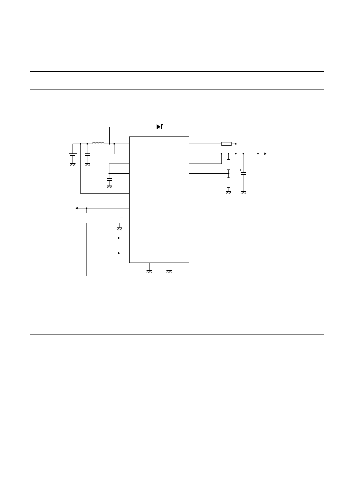
Fig.5 Application in 1-cell NiCd or NiMH battery powered equipment.
2002 May 14 12
Page 13
Philips Semiconductors Product specification
0.95 V starting DC-to-DC converter
with low battery indicator
handbook, full pagewidth
L1
C1
R8
R9
low-batt
C5
LX1
LX2
V
ref
V
ref
LBI1
U/D
LBO
1
16
7
11
9
TEA1200TS
15
10
D1
ILIM
5
UPOUT/DNIN
4
UPOUT/DNIN
3
FB0
12
R
ILIM
R1
R2
C2
TEA1200TS
V
out_dcdc
SYNC/PWM
SHDWN0
R7
14
2
813
GND GND0
MBL420
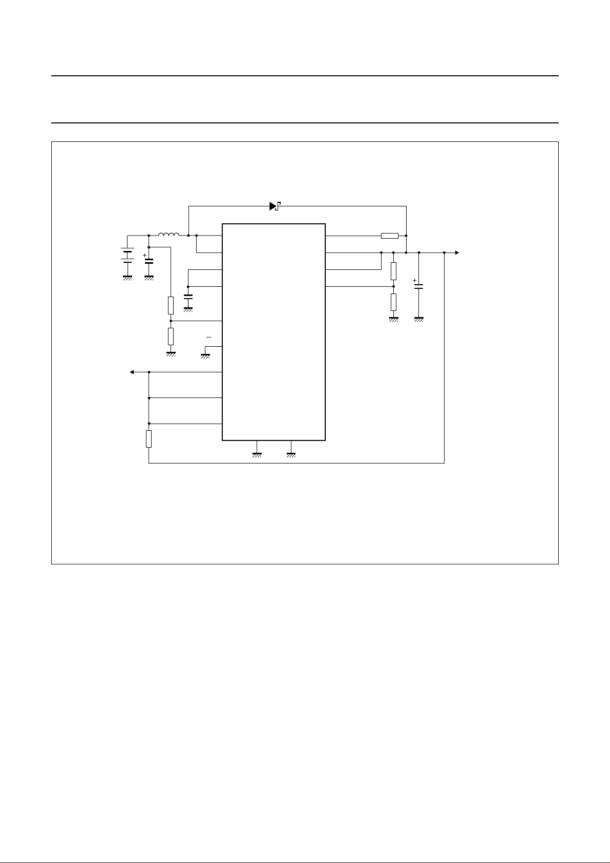
Fig.6 Application in 2-cell NiCd or NiMH battery poweredequipment with autonomous shut-down at low battery
voltage.
2002 May 14 13
Page 14
Philips Semiconductors Product specification
0.95 V starting DC-to-DC converter
with low battery indicator
handbook, full pagewidth
C1
R7
low-batt
UPOUT/DNIN
UPOUT/DNIN
R
R8
R9
SYNC/PWM
ILIM
ILIM
C5
LBI1
LBO
SHDWN0
V
V
U/D
4
3
5
ref
7
ref
11
15
9
10
14
2
GND GND0
TEA1200TS
813
TEA1200TS
LX1
1
LX2
16
FB0
12
MBL422
D1
L1
R1
R2
C2
V
out_dcdc
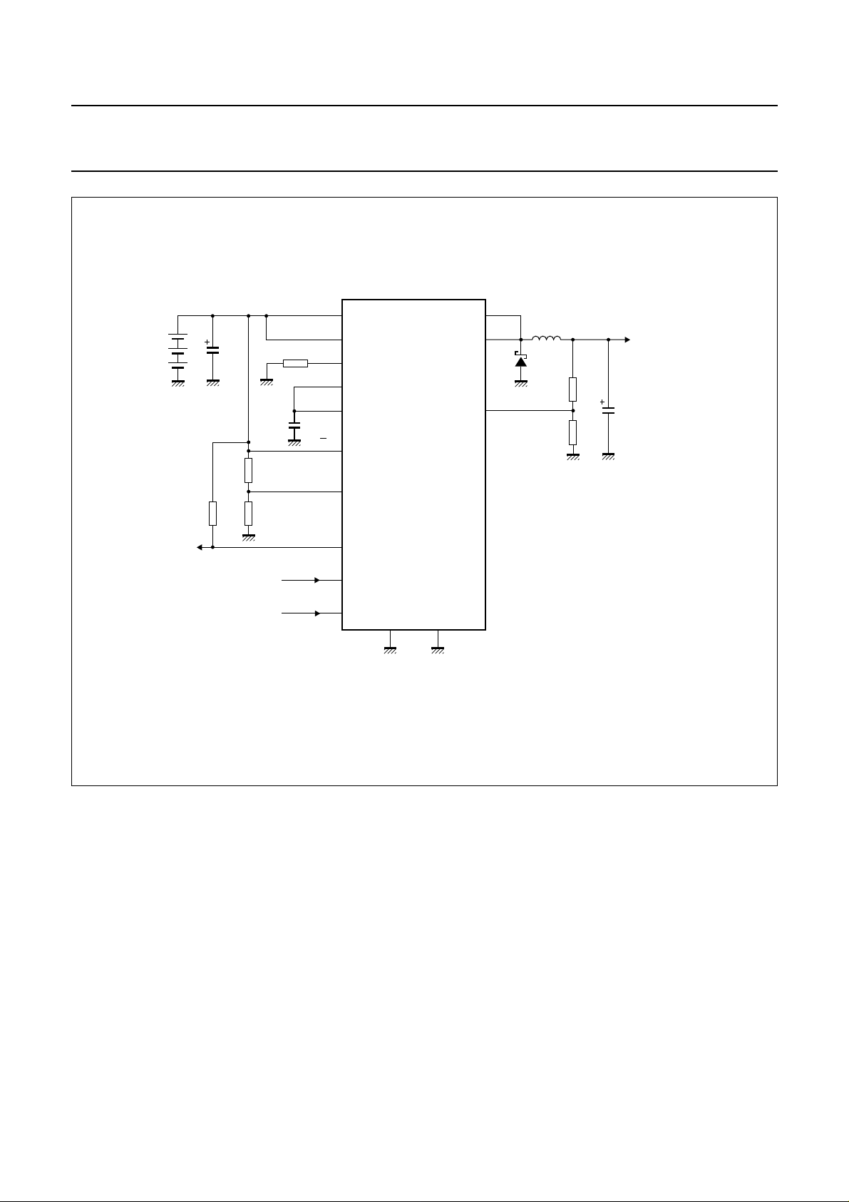
Fig.7 Application in 3-cell NiCd or NiMH and 1-cell Li-Ion battery powered equipment.
2002 May 14 14
Page 15

Philips Semiconductors Product specification
0.95 V starting DC-to-DC converter
with low battery indicator
External component selection
INDUCTOR L1
The performance of the TEA1200TS is not very sensitive
to inductance value. The best efficiency performance over
a wide load current range is achieved by using an
inductance of 6.8 µH e.g. TDK SLF7032 or Coilcraft
DO1608 range.
DC-TO-DC CONVERTER INPUT CAPACITOR C1
The value of C1 strongly depends on the type of input
source. In general, a 100 µF tantalum capacitor is
sufficient.
DC-TO-DC CONVERTER OUTPUT CAPACITOR C2
Thevalue and typeof C2depends on the maximumoutput
current and the ripple voltage which is allowed in the
application. Low-ESR tantalum capacitors show good
results. The most important specification of C2 is its ESR,
which mainly determines the output voltage ripple.
TEA1200TS
CURRENT LIMITING RESISTOR R10
The maximum instantaneous current is set by the external
resistor R10. The preferred type is SMD, with 1%
accuracy.
The connection of resistor R10 differs for each mode:
• At upconversion: resistor R10 must be connected
between pins ILIM and UPOUT/DNIN; the current
320
limiting level is defined by:
• At downconversion: resistor R10 must be connected
between pins ILIM and GND0; the current limiting level
300
I
is defined by:
Iim
=
----------R10
The average inductor current during limited current
operation also depends on the inductance value, input
voltage, output voltage and resistive losses in all
components in the power path. Ensure that
I
lim<Isat
(saturation current) of the inductor.
=
I
-----------
Iim
R10
DIODE D1
The Schottky diode is only used for short time during
takeover from N-type power MOSFET and P-type power
MOSFET and vice versa. Therefore, a medium-power
diode is sufficient in most applications e.g. Philips
PRLL5819.
FEEDBACK RESISTORS R1 AND R2
The output voltage of the DC-to-DC converter is
determined by the resistors R1 and R2. The following
conditions apply:
• Only use a 1% accurate SMD type resistors. If larger
body-size resistors are used, the capacitance on
pin FB0 will be too large, and could cause inaccurate
operation.
• Resistors R1 and R2 should have a maximum value of
50 kΩ when connected in parallel. A higher value will
result in inaccurate operation.
Under these conditions, the output voltage can be
calculated by the following equation:
R1
V
=
o
V
×
ref
1
+
------- -
R2
REFERENCE VOLTAGE DECOUPLING CAPACITOR C5
Optionally, a decoupling capacitor can be connected
between pin V
and ground in order to achieve a lower
ref
noise level of the output voltages of the LDO. The best
choice for C5 is a ceramic multilayer capacitor of
approximately 10 nF.
LOW BATTERY DETECTOR COMPONENTS R7, R8 AND R9
Resistor R7 is connected between pin LBO and the input
or output pin and must be 330 kΩ or higher.
A 1-cell NiCd or NiMHbattery canbe connected directly to
pin LBI1.
A higher battery voltage can be detected by application of
a divider circuit with resistor R8 and R9. The low-battery
detection level for a higher battery voltage can be set by
using the following equation:
V
LBI det )()
V
det
R9
×=
--------------------------R8 R9+()
Sincecurrent flows intopinLBI1, the parallel impedanceof
R8 and R9 must be approximately 1 kΩ in order to avoid
inaccuracy due to the spread of the LBI1 current.
2002 May 14 15
Page 16
Philips Semiconductors Product specification
0.95 V starting DC-to-DC converter
with low battery indicator
100
handbook, full pagewidth
η
(%)
80
60
40
110
TEA1200TS
MGU577
(1)
(2)
2
10
IL (mA)
3
10
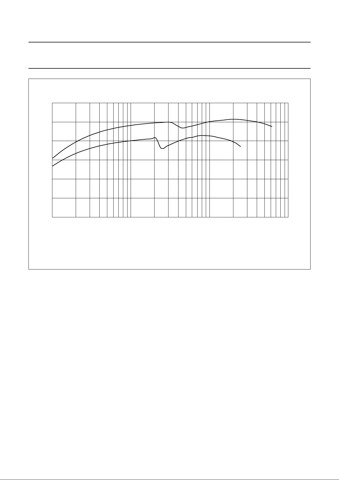
(1) VI= 2.4 V.
(2) VI= 1.2 V.
VO= 3.5 V
Fig.8 Efficiency as a function of load current.
2002 May 14 16
Page 17
Philips Semiconductors Product specification
0.95 V starting DC-to-DC converter
with low battery indicator
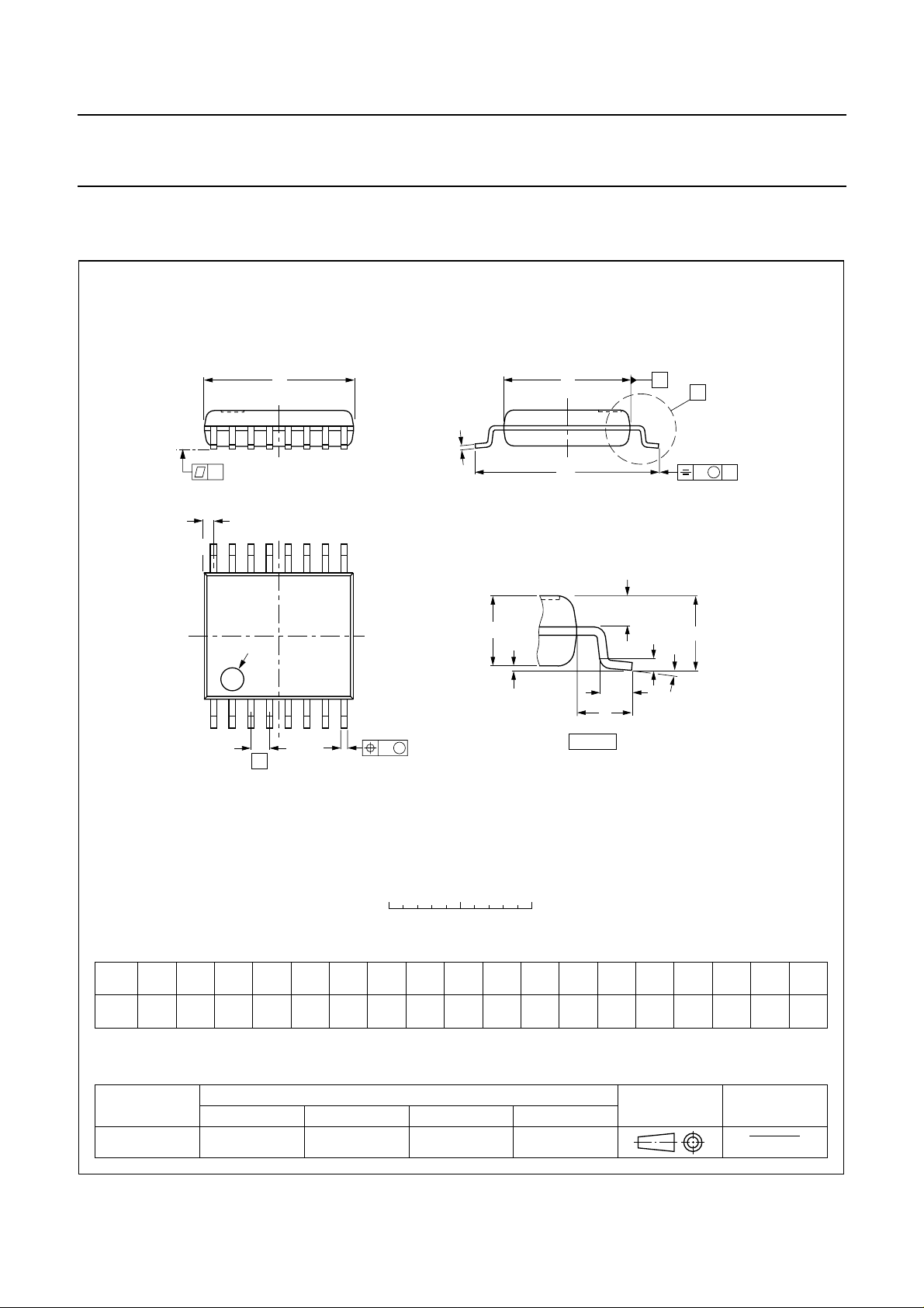
PACKAGE OUTLINE
SSOP16: plastic shrink small outline package; 16 leads; body width 4.4 mm
16
D
c
y
Z
9
E
H
E
TEA1200TS
SOT369-1
A
X
v M
A
pin 1 index
18
w M
b
b
0.32
0.20
p
p
0 2.5 5 mm
scale
(1)E(1)
cD
0.25
5.30
5.10
4.5
4.3
0.13
eHELLpQZywv θ
0.65
e
DIMENSIONS (mm are the original dimensions)
UNIT A
mm
Note
1. Plastic or metal protrusions of 0.20 mm maximum per side are not included.
A
max.
1.5
0.15
0.00
1
A2A
1.4
1.2
3
0.25
Q
A
2
6.6
6.2
L
0.65
0.45
(A )
L
p
A
1
detail X
0.75
1.0
0.45
3
A
θ
0.130.2 0.1
0.48
0.18
(1)
o
10
o
0
OUTLINE
VERSION
SOT369-1 MO-152
IEC JEDEC EIAJ
REFERENCES
2002 May 14 17
EUROPEAN
PROJECTION
ISSUE DATE
95-02-04
99-12-27
Page 18

Philips Semiconductors Product specification
0.95 V starting DC-to-DC converter
with low battery indicator
SOLDERING
Introduction to soldering surface mount packages
Thistext gives a verybriefinsight to a complextechnology.
A more in-depth account of soldering ICs can be found in
our
“Data Handbook IC26; Integrated Circuit Packages”
(document order number 9398 652 90011).
There is no soldering method that is ideal for all surface
mount IC packages. Wave soldering can still be used for
certainsurface mount ICs, butitisnot suitable for finepitch
SMDs. In these situations reflow soldering is
recommended.
Reflow soldering
Reflow soldering requires solder paste (a suspension of
fine solder particles, flux and binding agent) to be applied
tothe printed-circuit boardby screen printing, stencillingor
pressure-syringe dispensing before package placement.
Several methods exist for reflowing; for example,
convection or convection/infrared heating in a conveyor
type oven. Throughput times (preheating, soldering and
cooling) vary between 100 and 200 seconds depending
on heating method.
Typical reflow peak temperatures range from
215 to 250 °C. The top-surface temperature of the
packages should preferable be kept below 220 °C for
thick/large packages, and below 235 °C for small/thin
packages.
Wave soldering
Conventional single wave soldering is not recommended
forsurface mount devices (SMDs)orprinted-circuitboards
with a high component density, as solder bridging and
non-wetting can present major problems.
To overcome these problems the double-wave soldering
method was specifically developed.
TEA1200TS
• Use a double-wave soldering method comprising a
turbulent wave with high upward pressure followed by a
smooth laminar wave.
• For packages with leads on two sides and a pitch (e):
– larger than or equal to 1.27 mm, the footprint
longitudinal axis is preferred to be parallel to the
transport direction of the printed-circuit board;
– smaller than 1.27 mm, the footprint longitudinal axis
must be parallel to the transport direction of the
printed-circuit board.
The footprint must incorporate solder thieves at the
downstream end.
• Forpackages with leads onfoursides,the footprint must
be placed at a 45° angle to the transport direction of the
printed-circuit board. The footprint must incorporate
solder thieves downstream and at the side corners.
During placement andbefore soldering,the packagemust
be fixed with a droplet of adhesive. The adhesive can be
applied by screen printing, pin transfer or syringe
dispensing. The package can be soldered after the
adhesive is cured.
Typical dwell time is 4 seconds at 250 °C.
A mildly-activated flux will eliminate the need for removal
of corrosive residues in most applications.
Manual soldering
Fix the component by first soldering two
diagonally-opposite end leads. Use a low voltage (24 V or
less) soldering iron applied to the flat part of the lead.
Contact time must be limited to 10 seconds at up to
300 °C.
When using a dedicated tool, all other leads can be
soldered in one operation within 2 to 5 seconds between
270 and 320 °C.
If wave soldering is used the following conditions must be
observed for optimal results:
2002 May 14 18
Page 19

Philips Semiconductors Product specification
0.95 V starting DC-to-DC converter
TEA1200TS
with low battery indicator
Suitability of surface mount IC packages for wave and reflow soldering methods
PACKAGE
BGA, HBGA, LFBGA, SQFP, TFBGA not suitable suitable
HBCC, HLQFP, HSQFP, HSOP, HTQFP, HTSSOP, HVQFN, SMS not suitable
(3)
PLCC
LQFP, QFP, TQFP not recommended
SSOP, TSSOP, VSO not recommended
Notes
1. All surface mount (SMD) packages are moisture sensitive. Depending upon the moisture content, the maximum
2. These packages are not suitable for wave soldering. On versions with the heatsink on the bottom side, the solder
3. If wave soldering is considered, then the package must be placed at a 45° angle to the solder wave direction.
4. Wave soldering is only suitable for LQFP, TQFP and QFP packages with a pitch (e) equal to or larger than 0.8 mm;
5. Wave soldering is only suitable forSSOP and TSSOP packages with a pitch (e) equal to orlarger than 0.65 mm; it is
, SO, SOJ suitable suitable
temperature (with respect to time) and body size of the package, there is a risk that internal or external package
cracks may occur due to vaporization of the moisture in them (the so called popcorn effect). For details, refer to the
Drypack information in the
cannot penetrate between the printed-circuit board and the heatsink. On versions with the heatsink on the top side,
the solder might be deposited on the heatsink surface.
The package footprint must incorporate solder thieves downstream and at the side corners.
it is definitely not suitable for packages with a pitch (e) equal to or smaller than 0.65 mm.
definitely not suitable for packages with a pitch (e) equal to or smaller than 0.5 mm.
“Data Handbook IC26; Integrated Circuit Packages; Section: Packing Methods”
SOLDERING METHOD
WAVE REFLOW
(2)
(3)(4)
(5)
suitable
suitable
suitable
(1)
.
2002 May 14 19
Page 20

Philips Semiconductors Product specification
0.95 V starting DC-to-DC converter
TEA1200TS
with low battery indicator
DATA SHEET STATUS
PRODUCT
DATA SHEET STATUS
Objective data Development This data sheet contains data from the objective specification for product
Preliminary data Qualification This data sheet contains data from the preliminary specification.
Product data Production This data sheet contains data from the product specification. Philips
Notes
1. Please consult the most recently issued data sheet before initiating or completing a design.
2. The product status of the device(s) described in this data sheet may have changed since this data sheet was
published. The latest information is available on the Internet at URL http://www.semiconductors.philips.com.
(1)
STATUS
(2)
development. Philips Semiconductors reserves the right to change the
specification in any manner without notice.
Supplementary data will be published at a later date. Philips
Semiconductors reserves the right to change the specification without
notice, in order to improve the design and supply the best possible
product.
Semiconductors reserves the right to make changes at any time in order
to improve the design, manufacturing and supply. Changes will be
communicated according to the Customer Product/Process Change
Notification (CPCN) procedure SNW-SQ-650A.
DEFINITIONS
DEFINITIONS
Short-form specification The data in a short-form
specification is extracted from a full data sheet with the
same type number and title. For detailed information see
the relevant data sheet or data handbook.
Limiting values definition Limiting values given are in
accordance with the Absolute Maximum Rating System
(IEC 60134). Stress above one or more of the limiting
values may cause permanent damage to the device.
These are stress ratings only and operation of the device
atthese or at anyotherconditions above thosegivenin the
Characteristics sections of the specification is not implied.
Exposure to limiting values for extended periods may
affect device reliability.
Application information Applications that are
described herein for any of these products are for
illustrative purposes only. Philips Semiconductors make
norepresentationor warranty that suchapplicationswillbe
suitable for the specified use without further testing or
modification.
DISCLAIMERS
Life support applications These products are not
designed for use in life support appliances, devices, or
systems where malfunction of these products can
reasonably be expectedto result in personal injury.Philips
Semiconductorscustomersusing or selling theseproducts
for use in such applications do so at their own risk and
agree to fully indemnify Philips Semiconductors for any
damages resulting from such application.
Right to make changes Philips Semiconductors
reserves the right to make changes, without notice, in the
products, including circuits, standard cells, and/or
software, described or contained herein in order to
improve design and/or performance. Philips
Semiconductors assumes no responsibility or liability for
theuse of any oftheseproducts,conveys no licence ortitle
under any patent, copyright, or mask work right to these
products,and makes norepresentationsor warranties that
these products are free from patent, copyright, or mask
work right infringement, unless otherwise specified.
2002 May 14 20
Page 21

Philips Semiconductors Product specification
0.95 V starting DC-to-DC converter
with low battery indicator
TEA1200TS
NOTES
2002 May 14 21
Page 22

Philips Semiconductors Product specification
0.95 V starting DC-to-DC converter
with low battery indicator
TEA1200TS
NOTES
2002 May 14 22
Page 23

Philips Semiconductors Product specification
0.95 V starting DC-to-DC converter
with low battery indicator
TEA1200TS
NOTES
2002 May 14 23
Page 24

Philips Semiconductors – a w orldwide compan y
Contact information
For additional information please visit http://www.semiconductors.philips.com. Fax: +31 40 27 24825
For sales offices addresses send e-mail to: [email protected].
© Koninklijke Philips Electronics N.V. 2002
All rights are reserved. Reproduction in whole or in part is prohibited without the prior written consent of the copyright owner.
The information presented in this document does not form part of any quotation or contract, is believed to be accurate and reliable and may be changed
without notice. No liability will be accepted by the publisher for any consequence of its use. Publication thereof does not convey nor imply any license
under patent- or other industrial or intellectual property rights.
Printed in The Netherlands 403502/01/pp24 Date of release: 2002 May 14 Document order number: 9397 750 09358
SCA74
 Loading...