

Philips tea1093 DATASHEETS

INTEGRATED CIRCUITS
DATA SH EET
TEA1093
Hands-free IC
Product specification
Supersedes data of 1995 May 18
File under Integrated Circuits, IC03
1996 Feb 09

Philips Semiconductors Product specification
Hands-free IC TEA1093
FEATURES
• Line powered supply with:
– adjustable stabilized supply voltage
– power down function
• Microphone channel with:
– externally adjustable gain
– microphone mute function
• Loudspeaker channel with:
– externally adjustable gain
– dynamic limiter to prevent distortion
– rail-to-rail output stages for single-ended or
bridge-tied load drive
– logarithmic volume control via linear potentiometer
– loudspeaker mute function
• Duplex controller consisting of:
– signal envelope and noise envelope monitors for both
channels with:
externally adjustable sensitivity
externally adjustable signal envelope time constant
externally adjustable noise envelope time constant
– decision logic with:
externally adjustable switch-over timing
externally adjustable idle mode timing
externally adjustable dial tone detector in receive
channel
– voice switch control with:
adjustable switching range
constant sum of gain during switching
constant sum of gain at different volume settings.
APPLICATIONS
• Line-powered telephone sets with
hands-free/listening-in functions.
GENERAL DESCRIPTION
The TEA1093 is a bipolar circuit intended for use in
line-powered telephone sets. In conjunction with a
member of the TEA1060 family or PCA1070 transmission
circuits, the device offers a hands-free function for line
powered telephone sets. It incorporates a supply, a
microphone channel, a loudspeaker channel and a duplex
controller with signal and noise monitors on both channels.
ORDERING INFORMATION
TYPE NUMBER
NAME DESCRIPTION VERSION
TEA1093 DIP28 plastic dual in-line package; 28 leads (600 mil) SOT117-1
TEA1093T SO28 plastic small outline package; 28 leads; body width 7.5 mm SOT136-1
1996 Feb 09 2
PACKAGE
Philips Semiconductors Product specification
Hands-free IC TEA1093
QUICK REFERENCE DATA
V
= 4.2 V; V
SREF
RL=50Ω; R
VOL
SYMBOL PARAMETER CONDITIONS MIN. TYP. MAX. UNIT
I
SUP
V
BB
I
BB(pd)
operating supply current (pin SUP) 7 − 140 mA
stabilized supply voltage 3.35 3.6 3.85 V
current consumption from pin VBB in
power-down condition
I
SUP(pd)
current consumption from pin SUP in
power-down condition
G
vtx
voltage gain from pin MIC to pin MOUT in
transmit mode
∆G
G
∆G
V
O(p-p)
vtxr
vrx
vrxr
voltage gain adjustment with R
voltage gain in receive mode V
voltage gain adjustment with R
bridge-tied load (peak-to-peak value) V
SWRA switching range − 40 − dB
∆SWRA switching range adjustment with R
referenced to R
T
amb
operating ambient temperature −25 − +75 °C
GND
=0V; I
= 15 mA; V
SUP
= 0 V (RMS); f = 1 kHz; T
SUP
=25°C; PD=LOW; MUTET = LOW;
amb
=0Ω; measured in test circuit of Fig.15; unless otherwise specified.
PD = HIGH; VBB= 3.6 V − 400 550 µA
GAT
the difference between RIN1 and RIN2
to LSP1 or LSP2 single-ended load
PD = HIGH; V
V
= 1 mV (RMS);
MIC
R
= 30.1 kΩ
GAT
= 20 mV (RMS);
RIN
R
= 66.5 kΩ;
GAR
RL=50Ω
= 4.5 V − 55 75 µA
sup
the difference between RIN1 and RIN2
to the difference between LSP1 and
LSP2 bridge-tied load
GAR
= 150 mV (RMS);
RIN
RL=33Ω; note 1
SWR
= 365 kΩ
SWR
12.5 15 17.5 dB
−10 − +10 dB
15.5 18 20.5 dB
21.5 24 26.5 dB
−15 − +15 dB
− 5.15 − V
−40 − +12 dB
Note
1. Corresponds to 100 mW output power.
1996 Feb 09 3
Philips Semiconductors Product specification
Hands-free IC TEA1093
BLOCK DIAGRAM
handbook, full pagewidth
TEA106X
TEA106X
V
BB
R
C
TSEN
C
TENV
C
TNOI
C
RNOI
C
RENV
to
to
C
MIC
MIC
R
TSEN
C
SUP
9
315 mV
7
SREF
19
MUTET
22
MIC
28
TSEN
V V
MICROPHONE CHANNEL
V I
DUPLEX CONTROLLER
LOG
TR1
SWITCH
SUPPLY
TR2
to dynamic
limiter
VOLTAGE
STABILIZER
POWER
DOWN
I V
TEA1093
BUFFER
27
TENV
13
mV
26
TNOI
23
RNOI
24
RENV
BUFFER
BUFFER
BUFFER
ATTENUATOR
13 mV
LOGIC
VOICE
SWITCH
V
BB
PD
VA
GAT
MOUT
MICGND
IDT
V
ref
SWT
STAB
SWR
10
17
15
8GND
21
20
18
16
14
13
12
VBB
R
GAT
to TEA106X
R
IDT
C
SWT
R
STAB
R
SWR
R
RSEN
25
C
C
RSEN
LSP1
R
GAR
C
DLC
RSEN
GAR
5
LSP1
6
DLC/
1
MUTER
4
LSP2
from voltage
stabilizer
DYNAMIC
LIMITER
LOG
V
dt
−1
LOUDSPEAKER CHANNEL
Fig.1 Block diagram.
1996 Feb 09 4
V I
I V
VOLUME
CONTROL
2
RIN1
RIN2
VOL 11
2
3
from
TEA106X
from
TEA106X
R
MGD216
VOL
Philips Semiconductors Product specification
Hands-free IC TEA1093
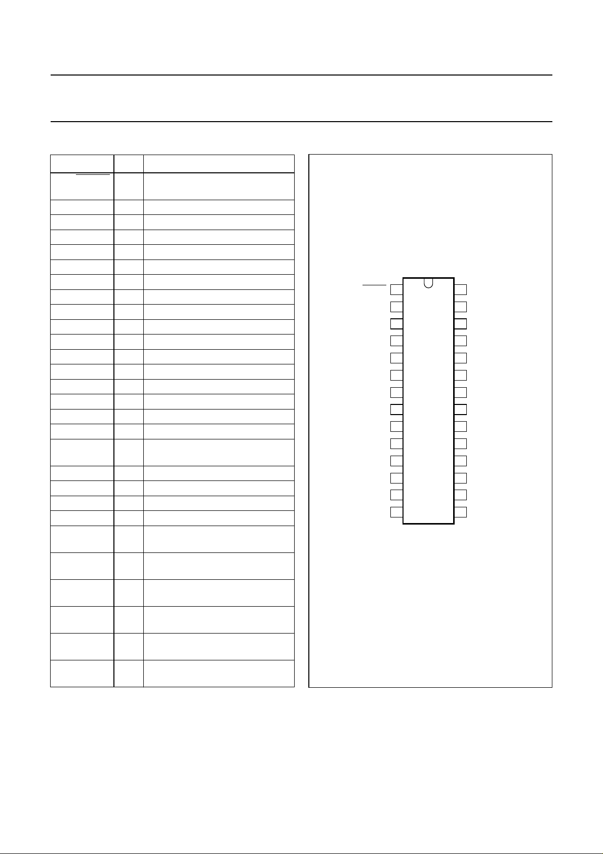
PINNING
SYMBOL PIN DESCRIPTION
MUTER 1 dynamic limiter timing adjustment,
DLC/
receiver channel mute input
RIN1 2 receiver amplifier input 1
RIN2 3 receiver amplifier input 2
LSP2 4 loudspeaker amplifier output 2
GAR 5 receiver gain adjustment
LSP1 6 loudspeaker amplifier output 1
SREF 7 supply reference input
GND 8 ground reference
SUP 9 supply input
V
BB
10 stabilized supply output
VOL 11 receiver volume adjustment
SWR 12 switching range adjustment
STAB 13 reference current adjustment
SWT 14 switch-over timing adjustment
VA 15 V
voltage adjustment
BB
IDT 16 idle mode timing adjustment
PD 17 power-down input
MICGND 18 ground reference for the
microphone amplifier
MUTET 19 transmit channel mute input
MOUT 20 microphone amplifier output
GAT 21 microphone gain adjustment
MIC 22 microphone input
RNOI 23 receive noise envelope timing
adjustment
RENV 24 receive signal envelope timing
adjustment
RSEN 25 receive signal envelope sensitivity
adjustment
TNOI 26 transmit noise envelope timing
adjustment
TENV 27 transmit signal envelope timing
adjustment
TSEN 28 transmit signal envelope
sensitivity adjustment
handbook, halfpage
DLC/MUTER
1
2
RIN1
3
RIN2
4
LSP2
5
GAR
6
LSP1
7
SREF
TEA1093
8
GND
9
SUP
10
V
BB
11
VOL
12
SWR
13
STAB
14
SWT
MGD217
Fig.2 Pin configuration.
28
27
26
25
24
23
22
21
20
19
18
17
16
15
TSEN
TENV
TNOI
RSEN
RENV
RNOI
MIC
GAT
MOUT
MUTET
MICGND
PD
IDT
VA
1996 Feb 09 5
Philips Semiconductors Product specification
Hands-free IC TEA1093
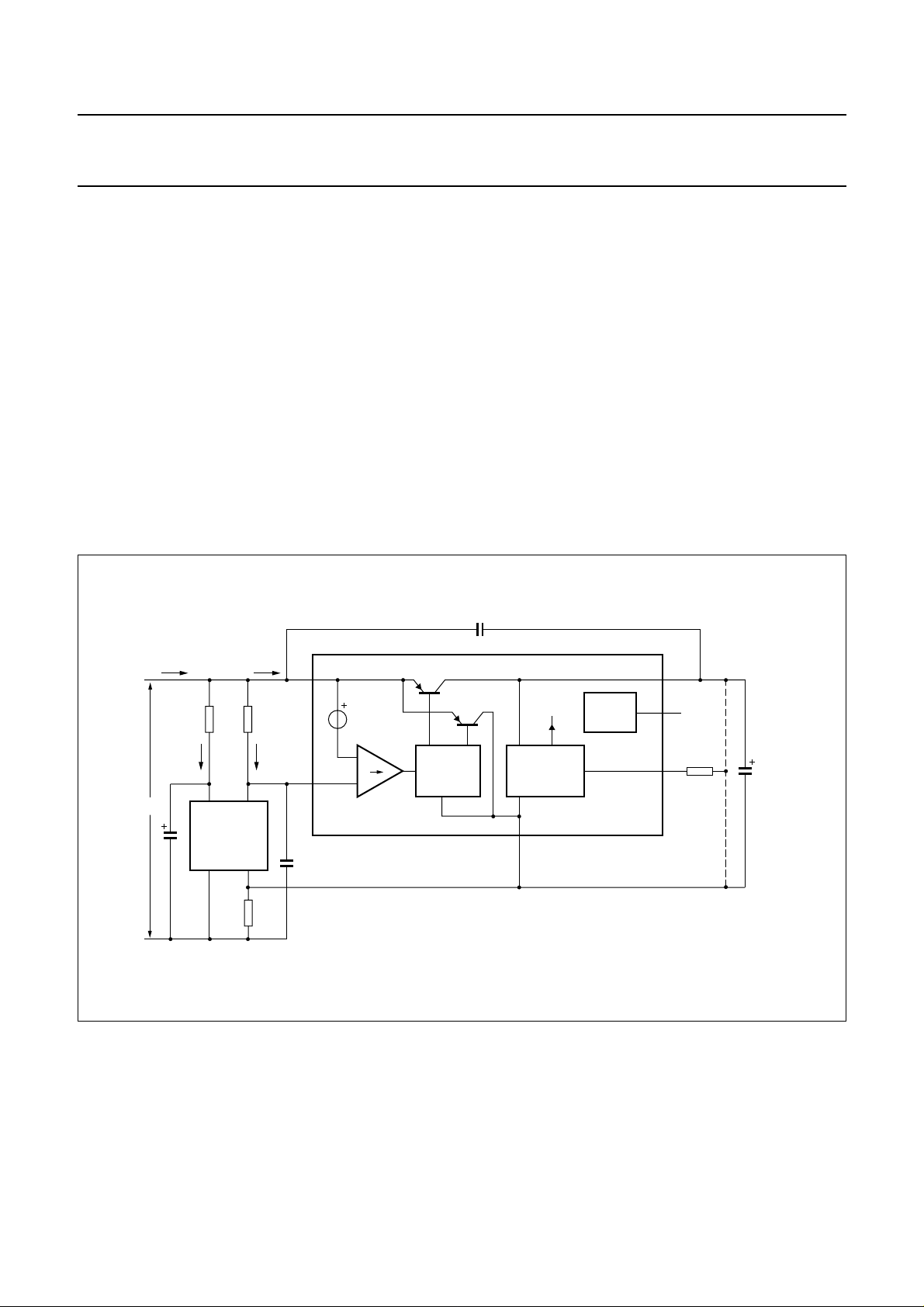
FUNCTIONAL DESCRIPTION
The values given in the functional description are typical
values except when otherwise specified.
A principle diagram of the TEA106X is shown on the left
side of Fig.3. The TEA106X is a transmission circuit of the
TEA1060 family intended for hand-set operation. It
incorporates a receiving amplifier for the earpiece, a
transmit amplifier for the microphone and a hybrid. For
more details on the TEA1060 family, please refer to
Handbook IC03”
. The right side of Fig.3 shows a principle
“Data
diagram of the TEA1093, a hands-free add-on circuit with
a microphone amplifier, a loudspeaker amplifier and a
duplex controller.
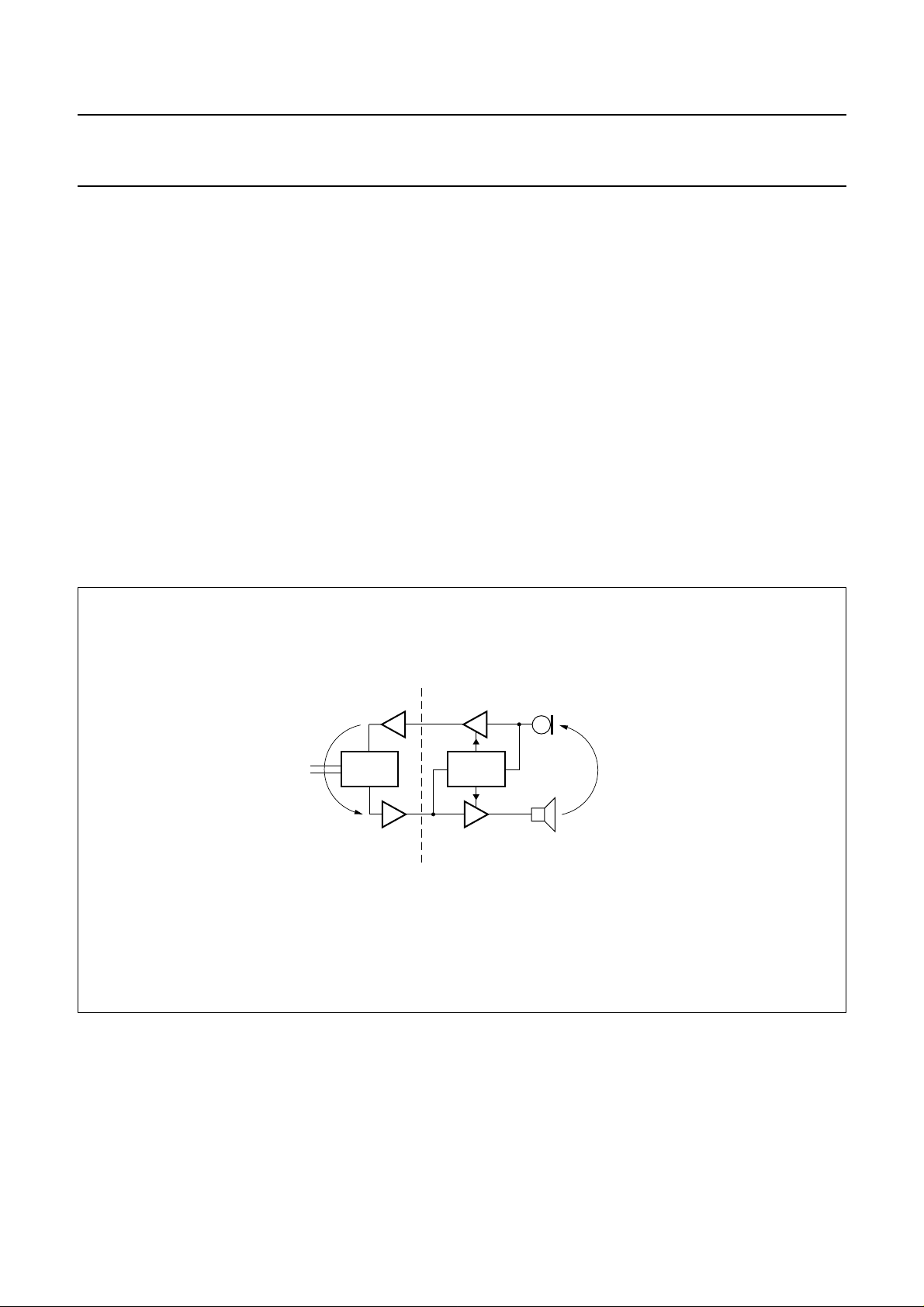
As can be seen from Fig.3, a loop is formed via the
sidetone network in the transmission circuit and the
acoustic coupling between loudspeaker and microphone
of the hands-free circuit. When this loop gain is greater
than 1, howling is introduced. In a full duplex application,
this would be the case. The loop-gain has to be much
lower than 1 and therefore has to be decreased to avoid
howling. This is achieved by the duplex controller.The
duplex controller of the TEA1093 detects which channel
has the ‘largest’ signal and then controls the gain of the
microphone amplifier and the loudspeaker amplifier so that
the sum of the gains remains constant. As a result, the
circuit can be in three stable modes:
1. Transmit mode (Tx mode): the gain of the microphone
amplifier is at its maximum and the gain of the
loudspeaker amplifier is at its minimum.
2. Receive mode (Rx mode): the gain of the loudspeaker
amplifier is at its maximum and the gain of the
microphone amplifier is at its minimum.
3. Idle mode: the gain of the amplifiers is halfway
between their maximum and minimum value.
The difference between the maximum gain and minimum
gain is called the switching range.
handbook, full pagewidth
telephone
line
HYBRID
sidetone
TEA106X TEA1093
DUPLEX
CONTROL
Fig.3 Hands-free telephone set principles.
acoustic
coupling
MGD218
1996 Feb 09 6
Philips Semiconductors Product specification
Hands-free IC TEA1093
Supply: pins SUP, SREF, VBB, GND, VA and PD
As can be seen from Fig.4, the line current is divided
between the speech-transmission circuit (I
the TEA1093 circuit (I
I
SUP=Iline
− ITR− I
). It can be shown that:
SUP
CC
TR+ICC
) and
Where:
ITR=V
V
SUP
R
SREF
SUP
− V
SREF
= 100 Ω
− V
SREF/RSREF
= 315 mV
ICC≈ 1mA
It follows that I
SUP
≈ I
LINE
− 4 mA.
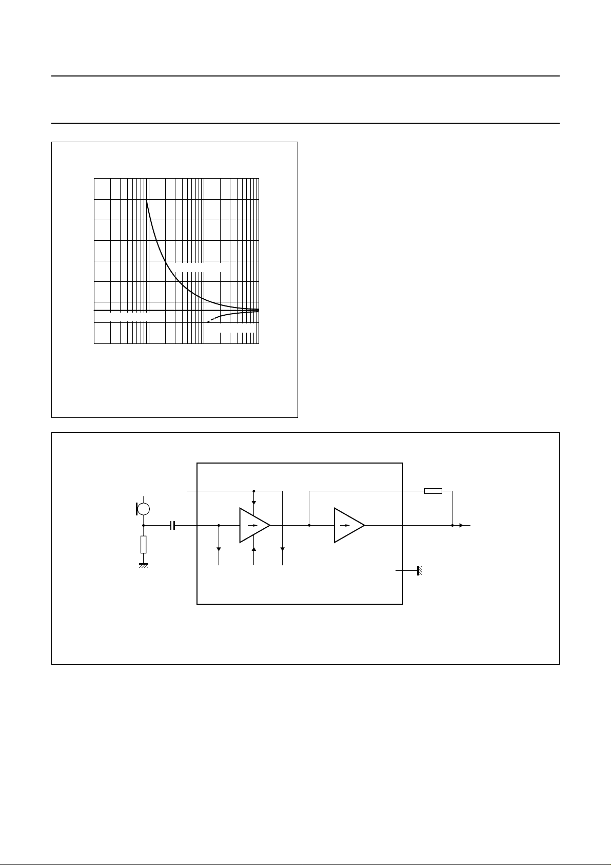
The TEA1093 stabilizes its own supply voltage of 3.6 V at
VBB. The voltage on VBB can be adjusted by means of an
external resistor RVA.
handbook, full pagewidth
I
I
line
SUP
R
SREF
100 Ω
ITR ICC
9
SUP
315 mV
V V
SREF
7
TR1
SWITCH
When R
is connected between pin VA and GND, the
VA
voltage on VBB is increased, when connected between
pin VA and VBB, it is decreased. This is shown in Fig.5.
Two capacitors of 4.7 nF (C
to ensure stability of the supply block. When V
greater than VBB+ 0.4 V, the current I
VBB via TR1. When V
is less, the current is shunted to
SUP
SREF
and C
) are required
STAB
is supplied to
SUP
SUP
is
GND via TR2, which prevents distortion on the line.
To reduce current consumption during pulse dialling or
register recall (flash), the TEA1093 is provided with a
power-down (PD) input. When the voltage on PD is HIGH,
the current consumption from SUP is 55 µA and from
VBB400 µA. Therefore a capacitor of 470 µF (C
VBB
sufficient to power the TEA1093 during pulse dialling.
C
STAB
4.7 nF
V
10
BB
TR2
to dynamic
limiter
VOLTAGE
STABILIZER
POWER
DOWN
PD
VA
17
R
VA
15
C
VBB
470 µF
) is
line
V
CC
LN
TEA1093
TEA106X
V
SLPE
EE
C
SREF
4.7 nF
Fig.4 Supply arrangement.
1996 Feb 09 7
GND
8
MGD219
Philips Semiconductors Product specification
Hands-free IC TEA1093
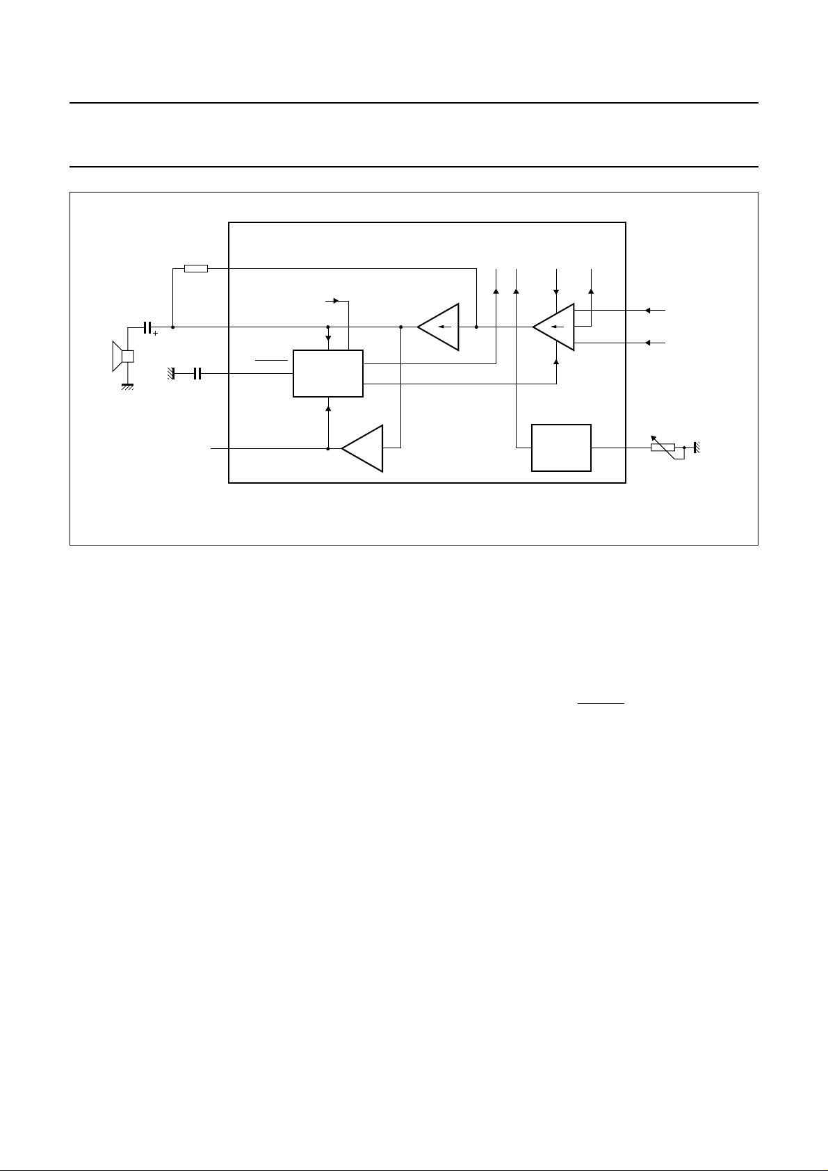
Microphone channel: pin MIC, GAT, MOUT, MICGND and MUTET
10
handbook, halfpage
V
BB
(V)
8
6
4
3.6 V without RVA
2
11010
RVA(VA-GND)
RVA(VA-VBB)
2103
RVA (kΩ)
Fig.5 VBB as a function of RVA.
MGD220
The TEA1093 has an asymmetrical microphone input MIC
with an input resistance of 20 kΩ. The gain of the input
stage varies according to the mode of the TEA1093. In the
transmit mode, the gain is at its maximum; in the receive
mode, it is at its minimum and in the idle mode, it is halfway
between maximum and minimum. Switch-over from one
mode to the other is smooth and click-free. The output
capability at pin MOUT is 20 µA (RMS).
In the transmit mode, the overall gain of the microphone
amplifier (from pin MIC to MOUT) can be adjusted from
5 dB up to 25 dB to suit specific application requirements.
The gain is proportional to the value of R
15 dB typical with R
= 30.1 kΩ.
GAT
A capacitor must be connected in parallel with R
and equals
GAT
GAT
to
ensure stability of the microphone amplifier. Together with
R
, it also provides a first-order low-pass filter.
GAT
By applying a HIGH level on pin MUTET, the microphone
amplifier is muted and the TEA1093 is automatically
forced into the receive mode.
handbook, full pagewidth
V
BB
R
MIC
R
19
MUTET
C
MIC
22
MIC
envelope
detector
V I I V
to
from
voice
switch
to
logic
GAT 21
MOUT
MICGND
MGD221
GAT
20
18
to TEA106X
Fig.6 Microphone channel.
1996 Feb 09 8
Philips Semiconductors Product specification
Hands-free IC TEA1093
handbook, full pagewidth
R
C
GAR
LSP1
C
DLC
GAR
5
LSP1
6
DLC/MUTER
1
4
LSP2
from voltage
stabilizer
DYNAMIC
LIMITER
−1
Fig.7 Loudspeaker channel.
Loudspeaker channel
L
OUDSPEAKER AMPLIFIER: PINS RIN1, RIN2, GAR, LSP1
AND LSP2
The TEA1093 has symmetrical inputs for the loudspeaker
amplifier with an input resistance of 40 kΩ between RIN1
and RIN2 (2 × 20 kΩ). The input stage can accommodate
signals up to 390 mV (RMS) at room temperature for 2% of
total harmonic distortion (THD). The gain of the input stage
varies according to the mode of the TEA1093. In the
receive mode, the gain is at its maximum; in the transmit
mode, it is at its minimum and in the idle mode, it is halfway
between maximum and minimum. Switch-over from one
mode to the other is smooth and click-free. The rail-to-rail
output stage is designed to power a loudspeaker which is
connected as a single-ended load (between LSP1 and
GND) or as a bridge-tied load (between LSP1 and LSP2).
In the receive mode, the overall gain of the loudspeaker
amplifier can be adjusted from 3 dB up to 39 dB to suit
specific application requirements. The gain from RIN1 or
RIN2 to LSP1 is proportional to the value of R
equals 18 dB with R
= 66.5 kΩ. The second output
GAR
GAR
and
LSP2 is in opposite phase with LSP1. Therefore, in the
basic application, the gain between RIN1-RIN2 to
LSP1-LSP2 equals 24 dB typical with R
A capacitor connected in parallel with R
= 66.5 kΩ.
GAR
can be used to
GAR
provide a first-order low-pass filter.
I V
to
envelope
detector
RIN1 2
RIN2
VOL
3
11
MGD222
from
TEA106X
R
VOL
to
to/from
logic
voice switch
V I
VOLUME
CONTROL
V
OLUME CONTROL: PIN VOL
The loudspeaker amplifier gain can be adjusted with the
potentiometer R
. A linear potentiometer can be used to
VOL
obtain logarithmic control of the gain at the loudspeaker
amplifier. Each 950 Ω increase of R
results in a gain
VOL
loss of 3 dB. The maximum gain reduction with the volume
control is internally limited to the switching range.
D
YNAMIC LIMITER: PIN DLC/MUTER
The dynamic limiter of the TEA1093 prevents clipping of
the loudspeaker output stages and protects the operation
of the circuit when the supply condition falls below a
certain level.
Hard clipping of the loudspeaker output stages is
prevented by rapidly reducing the gain when the output
stages start to saturate. The time in which gain reduction
is effected (clipping attack time) is approximately a few
milliseconds. The circuit stays in the reduced gain mode
until the peaks of the loudspeaker signals no longer cause
saturation. The gain of the loudspeaker amplifier then
returns to its normal value within the clipping release time
(typical 250 ms). Both attack and release times are
proportional to the value of the capacitor C
. The total
DLC
harmonic distortion of the loudspeaker output stages, in
reduced gain mode, stays below 5% up to 10 dB
(minimum) of input voltage overdrive [providing V
RIN
is
below 390 mV (RMS)].
1996 Feb 09 9
 Loading...