

Philips TEA1085T, TEA1085AT, TEA1085A, TEA1085 Datasheet

INTEGRATED CIRCUITS
DATA SH EET
TEA1085; TEA1085A
Listening-in circuit for line-powered
telephone sets
Preliminary specification
File under Integrated Circuits, IC03A
March 1992
Philips Semiconductors Preliminary specification
Listening-in circuit for line-powered
telephone sets
FEATURES
• Internal supply
optimum current split-up
- low constant current (adjustable) in transmission IC
- nearly all line current available for listening-in
adjustable supply voltage
• Loudspeaker amplifier
dynamic limiter providing low distortion and the
highest possible output power
SE or BTL drive for loudspeaker volume control by
potentiometer and/or logic inputs (e.g.
microcontroller drive)
fixed gain of 35 dB
• Larsen level limiter
low sensitivity for own speech due to 3rd-order filter
and attack delay
adjustable voltage thresholds
• Power down input
• MUTE input
TEA1085/TEA1085A
- clickfree switching between listening-in mode and
standby mode
TEA1085
- toggle function
- start-up in standby condition
TEA1085A
- logic level input
TEA1085; TEA1085A
GENERAL DESCRIPTION
The TEA1085 and TEA1085A are bipolar ICs which have
been designed for use in line-powered telephone sets and
provide a listening-in facility for the received line signal via
a loudspeaker. Nearly all the line current can be used for
powering the loudspeaker.
The circuits incorporate a supply circuit, loudspeaker
amplifier dynamic limiter, MUTE circuit, power-down
facility and logic inputs for gain setting. The devices also
incorporate a Larsen Level Limiter to reduce howling
effects.
The ICs are intended for use in conjunction with a
transmission circuit of the TEA1060 family.
ORDERING INFORMATION
EXTENDED TYPE
NUMBER
TEA1085/TEA1085A 24 DIL plastic SOT101B
TEA1085T/TEA1085AT 24 SO24 plastic SOT137A
Notes
1. SOT101-1; 1998 Jun 18.
2. SOT137-1; 1998 Jun 18.
March 1992 2
PINS PIN POSITION MATERIAL CODE
PACKAGE
(1)
(2)
Philips Semiconductors Preliminary specification
Listening-in circuit for line-powered
TEA1085; TEA1085A
telephone sets
QUICK REFERENCE DATA
SYMBOL PARAMETER CONDITIONS MIN. TYP. MAX. UNIT
I
SUP
V
BB
I
SUP
G
v
∆G
v
I
SUP
t
ad(RMS)
V
DTI(RMS)
G
v
T
amb
input current range 4 − 120 mA
stabilized supply voltage − 3.6 − V
current consumption PD = HIGH − 55 −µA
voltage gain loudspeaker amplifier
SE − 35 − dB
BTL − 41 − dB
maximum gain reduction with logic
− 18 − dB
inputs (3 steps)
minimum input current
P
= 20 mW typ.
OUT
− 15 17 mA
into 50 Ω SE
P
= 40 mW typ.
OUT
−−32 mA
into 50 Ω BTL
Larsen limiter attack delay time V
DTI
100 − 200 ms
jumps from 0 to ≥ 100 mV (RMS value)
Larsen limiter threshold level Larsen mode − 7 − mV
Larsen limiter preamplifier gain setting
30 − 52 dB
range
operating ambient temperature range −25 −+75 °C
March 1992 3
This text is here in white to force landscape pages to be rotated correctly when browsing through the pdf in the Acrobat reader.This text is here in
n
_white to force landscape pages to be rotated correctly when browsing through the pdf in the Acrobat reader.This text is here inThis text is here in
white to force landscape pages to be rotated correctly when browsing through the pdf in the Acrobat reader. white to force landscape pages to be ...
March 1992 4
dbook, full pagewidth
Philips Semiconductors Preliminary specification
Listening-in circuit for line-powered
telephone sets
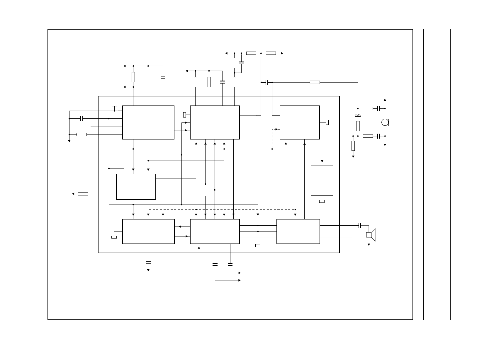
V
line
TEA1060
(LN)
V
1
SS
V
24
BB
19
PD
18
VA
(1)
V
BB
SREF
4
SUPPLY
4
SUP3SDC
2
PD
(1)
THL1
14
BB
THL212LLC
13
LARSEN
LEVEL
LIMITER
DCA
16
DTI
15
(1)
QLA
11
PREAMPLIFIER
LEVEL LIMITER
LARSEN
LAI−
109LAI+
TEA1060
(MIC)
TEA1060
(MIC)
V
BB
TEA1085
GSC1 8
GSC2 7
(1)
SIC 17
I-STABILIZATION
LOGIC GAIN
CONTROL
PEAK AND
CURRENT
LIMITER
2
2
2
RECEIVING
AMPLIFIER
MUTE
TEA1085A
POWER
AMPLIFIER
START
CIRCUIT
QLS1
2221QLS2
TEA1085; TEA1085A
(1) To TEA1060 (SLPE).
(2) See Fig.16.
23
DLC
(1)
20 5
MUTE LSI1 LSI2
(2)
6
MGR032
TEA1060 (VEE)
TEA1060 (QR)
(1)
Fig.1 Block diagram.
Philips Semiconductors Preliminary specification
Listening-in circuit for line-powered
telephone sets
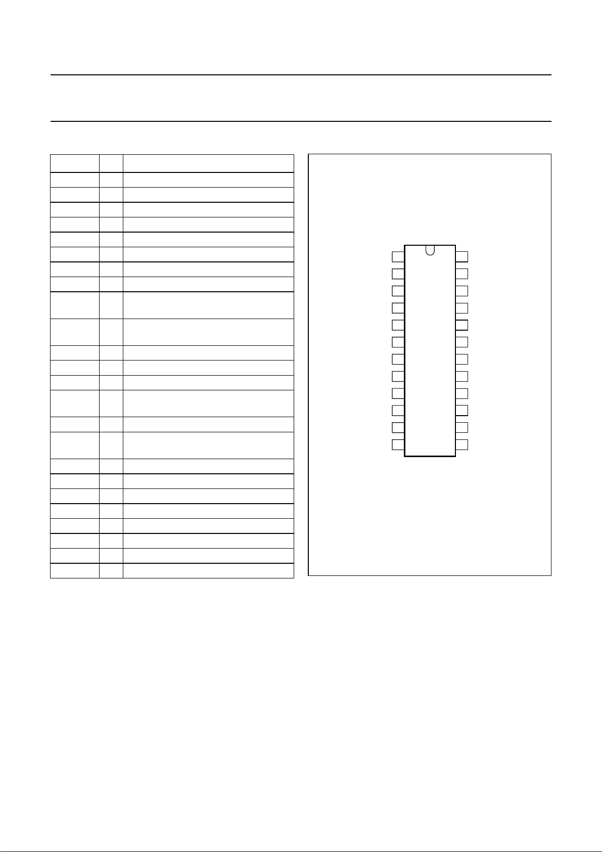
PIN CONFIGURATION
SYMBOL PIN DESCRIPTION
V
SS
SUP 2 positive supply
SDC 3 supply amplifier decoupling
SREF 4 supply reference input
LSI1 5 loudspeaker amplifier input 1
LSI2 6 loudspeaker amplifier input 2
GSC2 7 logic input 2 for gain select
GSC1 8 logic input 1 for gain select
LAI− 9 Larsen limiter preamplifier inverting
LAI+ 10 Larsen limiter preamplifier
QLA 11 Larsen limiter preamplifier output
LLC 12 Larsen limiter capacitor
THL2 13 Larsen limiter residual threshold level
THL1 14 Larsen limiter attack delay threshold
DTI 15 Larsen limiter detector input
DCA 16 Larsen limiter detector current
SIC 17 Larsen limiter current stabilizer
VA 18 V
PD 19 power-down input
MUTE 20 MUTE input
QLS1 21 loudspeaker amplifier output 1
QLS2 22 loudspeaker amplifier output 2
DLC 23 dynamic limiter capacitor
V
BB
1 negative supply
input
non-inverting input
level
adjustment
voltage adjustment
BB
24 stabilized supply decoupling
handbook, halfpage
TEA1085; TEA1085A
V
1
SS
SUP
2
SDC
3
SREF
4
LSI1
5
LSI2
6
TEA1085
GSC2
GSC1
LAI−
LAI+
QLA
LLC
TEA1085A
7
8
9
10
11
12
MLA415
Fig.2 Pin configuration.
V
24
BB
DLC
23
QLS2
22
QLS1
21
MUTE
20
19
PD
VA
18
17
SIC
DCA
16
DTI
15
THL1
14
THL2
13
March 1992 5
Philips Semiconductors Preliminary specification
Listening-in circuit for line-powered
telephone sets
FUNCTIONAL DESCRIPTION
Figure 1 illustrates a block diagram of the
TEA1085/TEA1085A with external components and
connections to the transmission IC.
The TEA1085/TEA1085A are bipolar ICs which have been
designed for use in line-powered telephone sets and
provide a listening-in facility for the received line signal via
a loudspeaker. Nearly all the line current can be used for
powering the loudspeaker.
The loudspeaker amplifier consists of a preamplifier, to
amplify the earpiece signal from the transmission circuit
and, a double push-pull output stage to drive the
loudspeaker in the BTL (bridge tied load) or SE (single
ended) configuration. The gain of the preamplifier is
controlled by a dynamic limiter which prevents high
distortion of the loudspeaker signal. This is achieved by
preventing clipping of the loudspeaker signal, with respect
to the supply voltage, and at too low supply current. Two
logic inputs can be used to reduce the gain in 3 steps.
Because of acoustic feedback from the loudspeaker to the
microphone, howling signals (Larsen effect) can occur on
the telephone line and in the loudspeaker. When the
Larsen signal exceeds a voltage and time duration
threshold the Larsen level limiter (LLL) will reduce the
TEA1085; TEA1085A
Larsen signal to a low level within a short period of time by
reducing the gain of the receiving preamplifier. This is
achieved by using the microphone signal as an input signal
which is processed in the LLL via a preamplifier and
3rd-order filter.
The MUTE input can be used to enable or disable the
loudspeaker amplifier.
The MUTE function of the TEA1085 has a toggle input to
permit the use of a simple push-button switch.
The MUTE function of the TEA1085A has a logic input to
operate with a microcontroller.
By activating the power-down input the current
consumption of the circuit will be reduced, this enables
pulse dialling or flash (register recall).
An internal start circuit ensures normal start-up of the
transmission IC and start-up of the listening-in IC in the
standby mode.
The TEA1085/TEA1085A are intended for use in
conjunction with a member of the TEA1060 family and
should be connected between LINE and SLPE of the
transmission IC. The transmission characteristics
(impedance, gain settings, for example) are not affected.
The interconnection between the two ICs is illustrated in
Fig.3.
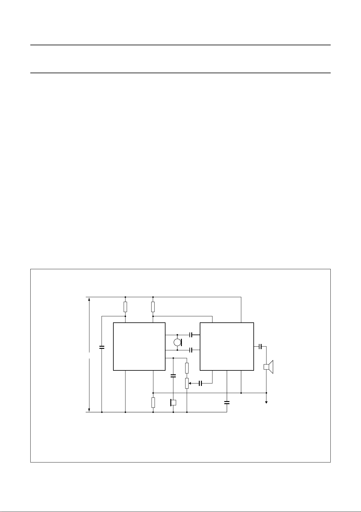
handbook, full pagewidth
LINE
V
CC
TEA1060
V
EE SLPE
LN
MIC+
MIC−
QR
Fig.3 Interconnection of the TEA1085/TEA1085A with the TEA1060.
March 1992 6
SREF SUP
LAI+
TEA1085
TEA1085A
LAI−
LSI1 LSI2
MGR033
QLS
V
SS
to TEA1060
(SLPE)
Philips Semiconductors Preliminary specification
Listening-in circuit for line-powered
telephone sets
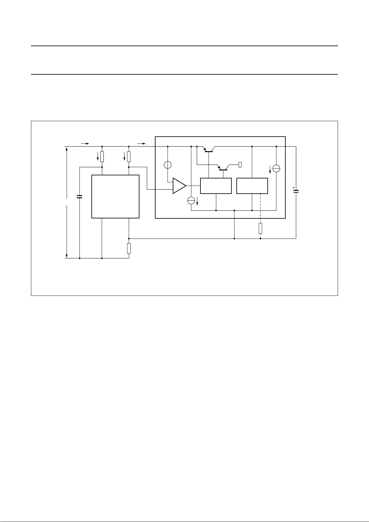
Supply; SUP, SREF, VBB, VSSand VA
The line current is divided into I
The supply arrangement is illustrated in Fig.4.
handbook, full pagewidth
LINE
I
line
I
CC
V
V
for the TEA1060 and I
TR
I
I
R1
CC
TEA1060
EE SLPE
TR
R20
LN
SUP
SUP
V
SREF
TEA1085
TEA1085A
for the TEA1085/TEA1085A.
SUP
TR1
int
I
TR2
BIAS
V
TEA1085; TEA1085A
V
BB
I
BBO
VOLTAGE
STABILIZER
SS
VA
R38
C20
R9
ITR is constant: ITR=V
/ R20; I
int
SUP=Iline
− ICC− I
TR
Fig.4 Supply arrangement.
Where:
V
int
is an internal temperature compensated
reference voltage with a typical value of
315 mV between SUP and SREF
R20 is a resistor between SUP and SREF
I
CC
is the internal current consumption of the
TEA106X (≈ 1 mA)
A practical value for R20 is 150 Ω. This value of resistance
produces a value for I
= 2 mA and I
TR
SUP
= I
line
− 3 mA.
The TEA1085/TEA1085A stabilizes its own supply voltage
at VBB. Transistor TR1 provides the supplies for the
internal circuits. TR2 is used to minimize the signal
distortion on the line by momentarily diverting the input
current to VSS whenever the instantaneous value of the
voltage V
drops below the supply voltage VBB. VBB is
SUP
fixed to a typical value of 3.6 V but can be increased by
means of an external resistor (R38) connected between
MGR034
VA and VSS or decreased by connecting this resistor
between VA and VBB. The minimum level on VBB is
restricted to 3.0 V; the level of the VBB limiter is also
affected (see application report for further information).
The supply at VBB is decoupled by a 470 µF capacitor.
The DC voltage (V
transmission IC (V
V
− VSS = V
SUP
LN−SLPE
− VSS) is determined by the
SUP
+ V
); thus:
.
int
LN−SLPE
The minimum DC voltage that can be applied to this input
is V
Where: V
BB(max)
+ 0.4 V.
is the worst case supply voltage (this
BB(max)
depends on the setting of R38, which is connected
between VA and VSS).
The internal current consumption of the
TEA1085/TEA1085A (I
V
− VSS = 4.5 V, MUTE off). Thus the current available
SUP
for powering the loudspeaker is I
The current I
consists of a bias current of ≈ 0.4 mA for
SUP0
the circuitry connected to SUP and current I
) is typically 4.2 mA (where
SUP0
− I
SUP0
.
BB0
SUP
of≈ 3.8 mA
which is used for the circuitry connected to VBB(see Fig.4).
March 1992 7
Philips Semiconductors Preliminary specification
Listening-in circuit for line-powered
telephone sets
5.5
dbook, halfpage
V
BB
(V)
5.1
4.7
4.3
3.9
3.5
10 10
2
R38 (kΩ)
MGR035
VBB = 3.60 V
3
10
TEA1085; TEA1085A
Logic gain control (GSC1 and GSC2) pins 7 and 8
The logic inputs GSC1 and GSC2 can be used to reduce
the gain of the loudspeaker amplifier by means of the logic
gain control function in 3 steps of 6 dB.
Table 1 Data for microcontroller drive of logic inputs
GSC2 GSC1
gain
(dB)
0 0 35 0
0 1 28.7 6.3
1 0 22.2 12.2
1 1 17 18
Where:
0 = connection to VSS or left open-circuit
1 = applying a voltage ≥ VSS+ 1.5 V
gain reduction
(dB)
Fig.5 Stabilized supply voltage as a function of
R38.
Supply amplifier stability (SDC) pin 3
To ensure stability of the TEA1085/TEA1085A, in
combination with a transmission IC of the TEA1060 family,
a 47 pF capacitor connected between SDC and SUP and
a 150 µH coil connected between SUP and the positive
line terminal (Fig.16) is required.
Loudspeaker amplifier (LSI1/LSI2 and QLS1/QLS2)
pins 5/6, 21/22
The TEA1085/TEA1085A have symmetrical inputs at LSI1
and LSI2. The input signal is normally taken from the
earpiece output of the transmission circuit via a resistive
attenuator (see Fig.3). The amount of attenuation must be
chosen in accordance with the receive gain of the
transmission IC (which depends on the sensitivity of the
earpiece transducer). The maximum input signal level is
450 mV(RMS) at T
= +25 °C.
amb
The outputs QLS1 and QLS2 can be used for single ended
drive (SE) or bridge tied load drive (BTL). The output
stages have been optimized for use with a 50 Ω
loudspeaker (e.g. Philips type AD2071).
The gain of the amplifier is fixed to ≈ 35 dB for the SE drive
and ≈ 41 dB for the BTL drive (when the inputs for logic
control are left open-circuit or are connected to VSS).
The volume control can be obtained by using a
potentiometer at the input and/or by the logic control
function.
March 1992 8
Philips Semiconductors Preliminary specification
Listening-in circuit for line-powered
telephone sets
Dynamic limiter (DLC) pin 23
To prevent distortion of the signal at the loudspeaker
outputs the gain of the amplifier is reduced rapidly when:
• the peaks of the signal at the loudspeaker outputs
exceed an internally determined threshold (voltage
limiter)
• the DC current into SUP is insufficient (current limiter)
• the voltage at VBB decreases below an internally
determined threshold, typically 2.9 V (VBB limiter)
The time in which the gain reduction is effected is the
'attack time'; this is very short in the first and third instance
and relatively long in the second instance. The circuit will
remain in the gain-reduced condition until the peaks of the
output signal remain below the threshold level. The gain
will then return to a nominal level after a time determined
by the capacitor connected to DLC (release time).
TEA1085; TEA1085A
MUTE input (MUTE) pin 20; TEA1085A
This MUTE is provided with a logic input to operate with a
microcontroller for instance.
The loudspeaker amplifier is disabled when the MUTE
input is LOW (connected to VSS or open input). A HIGH
level at the MUTE input enables the amplifier in the
listening-in mode.
MUTE input (MUTE) pin 20; TEA1085
The MUTE function is provided with a toggle input and is
designed to switch between the standby condition and the
listening-in condition on the rising edge of the input MUTE
signal (see Fig.6).
In the basic application the MUTE input must be LOW
(connected to V
operate the MUTE toggle (see Fig.7). Debouncing can be
realized by means of a small capacitor connected between
MUTE and VSS.
An internal start circuit ensures that the circuit always
starts up in the standby condition.
). A simple push-button can be used to
SS
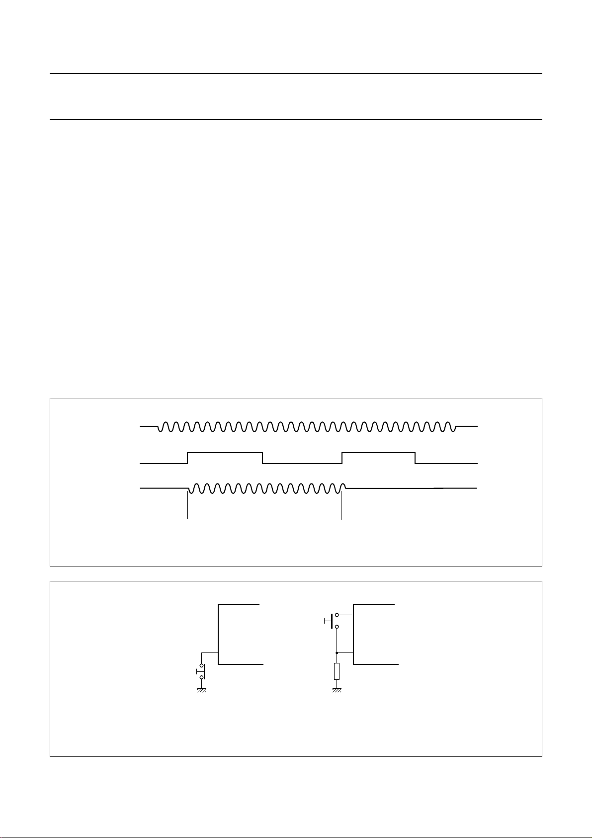
handbook, full pagewidth
handbook, full pagewidth
LSI1
MUTE
QLS1
standby standbylistening-in
Fig.6 Mute toggle function of the TEA1085.
MUTE MUTE
(a) Break contact. (b) Make contact.
10 kΩ
MGR036
V
BB
MLA055
Fig.7 Mute switch alternatives with the TEA1085.
March 1992 9
Philips Semiconductors Preliminary specification
Listening-in circuit for line-powered
telephone sets
Power down input (PD) pin 19
During pulse dialling or register recall (timed loop break)
the telephone line is interrupted, thereby breaking the
supply to the transmission and listening-in circuits. The
capacitor connected to VBB provides the supply for the
listening-in circuit during the supply breaks.
By making the PD input HIGH during the loop break the
requirement on the capacitor is eased and, consequently,
the internal (standby) current consumption I
VBB is reduced from 3.8 mA to 400 µA typical. So that the
transmission circuit is not affected transistors TR1 and
TR2 are inhibited and the bias current is reduced from
≈ 0.4 mA to ≈ 55 µA with V
= 4.5 V in the following
SUP
equation:
I
(where 4.2 V < V
SUP(PD)
= I
BIAS(PD)
= (V
< VBB+ 3 V)
SUP
− 2Vd) / Ra
SUP
2Vd = the voltage drop across 2 internal diodes (≈ 1.3 V)
Ra = an internal resistor of typical 60 kΩ
(Fig.4) at
BBO
TEA1085; TEA1085A
I
= 1.25 / R36; when R36 = 120 kΩ, I
SIC
Changing the value of R36 will affect the timing of the
Larsen level limiter system.
Larsen limiter preamplifier (LAI1/LAI2 and QLA) pins
9/10 and 11
This circuit amplifies the microphone signal to a level
suitable for the Larsen limiter detector. The gain is set by
external components (see Fig.8).
Normally the gain is set to the same level as the
microphone amplifier of the transmission circuit, this
ensures that the output signal level at output QLA is equal
to the line signal level.
The gain between QLA and the microphone input is given
by the following equation (the high-pass filter is not taken
into account):
A
pre
= V
/ VM = R29 / R26; in the basic application
QLA
R25 = R26 = 10 kΩ
= 10.5 µA
SIC
Larsen limiter current stabilizer (SIC) pin 17
A current reference is set by resistor R36 between SIC and
V
. The preferred value is 120 kΩ. The internal reference
SS
current is given by the following equation:
QLA
V
V
QLA
handbook, full pagewidth
R29
C23
R26
V
M
R25
C22
LAI−
LAI+
R28
R27
−
+
V
BB
The gain can be adjusted between 30 dB (R29 = 316 kΩ)
and 52 dB (R29 = 4 MΩ). The impedance result of R28 and
R27 in parallel must be equal to R29
(e.g. R27 = R28 = 2 × R29).
BB
R32C25
I
R30
DTI
−
+
LLC
C24
V
SS
R31
DCA
LARSEN
DETECTOR
THL1 THL2
R33
DCA
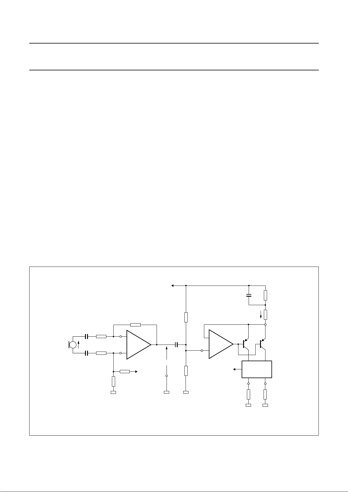
Fig.8 Larsen limiter preamplifier and voltage/current converter.
March 1992 10
R35 R34
MGR037
 Loading...