

Philips tea1083 DATASHEETS

INTEGRATED CIRCUITS
DATA SH EET
TEA1083; TEA1083A
Call progress monitor for line
powered telephone sets
Product specification
File under Integrated circuits, IC03A
March 1994
Philips Semiconductors Product specification
Call progress monitor for line powered
telephone sets
FEATURES
• Internal supply
– Optimum current split-up
– Low constant current (adjustable) in transmission IC
– Nearly all line current available for monitoring
– Stabilized supply voltage
• Loudspeaker amplifier with a fixed gain of 35 dB
• Volume controlled by potentiometer
• Power-down input (TEA1083A only)
• Loudspeaker enable input.
GENERAL DESCRIPTION
The TEA1083/83A is a bipolar IC which has been
designed for use in line powered telephone sets. It is
intended to offer a monitoring facility of the line signal via
TEA1083; TEA1083A
a loudspeaker during on-hook dialling. The TEA1083/83A
is intended for use in conjunction with a transmission
circuit of the TEA1060 family. The device uses a part of the
available line current via the internal supply circuit.
The loudspeaker amplifier, which consists of a preamplifier
and a power amplifier, amplifies the received line signals
from the transmission circuit when enabled via the LSE
input. The loudspeaker amplifier can also be used to
amplify dialling tones from the dialler IC. The power
amplifier contains a push-pull output stage to drive the
loudspeaker in a Single Ended Load (SEL) configuration.
The internal voltage stabilizer can be used to supply
external devices. By activating the power-down (PD) input
of the TEA1083A, the current consumption of the circuit
will be reduced, this enables pulse dialling or flash (register
recall).
An internal start circuit ensures normal start-up of the
transmission IC.
QUICK REFERENCE DATA
SYMBOL PARAMETER CONDITIONS MIN. TYP. MAX. UNIT
I
SUP
V
BB
I
SUP
G
v
I
SUP
T
amb
input current range 3.0 − 120 mA
stabilized supply current − 2.95 − V
current consumption PD = HIGH; TEA1083A only − 50 −µA
voltage gain of loudspeaker amplifier − 35 − dB
minimum input current PO = 10 mW (typ) into 50 Ω− 10 − mA
operating ambient temperature range −25 −+75 °C
ORDERING INFORMATION
EXTENDED TYPE
NUMBER
PINS PIN POSITION MATERIAL CODE
TEA1083 8 DIL PLASTIC SOT97D
TEA1083A 16 DIL PLASTIC SOT38
TEA1083AT 16 SOL PLASTIC SOT162AG
PACKAGE
(1)
(2)
(3)
Notes
1. SOT97-1; 1998 Jun 18.
2. SOT38-1; 1998 Jun 18.
3. SOT162-1; 1998 Jun 18.
March 1994 2
Philips Semiconductors Product specification
Call progress monitor for line powered
telephone sets
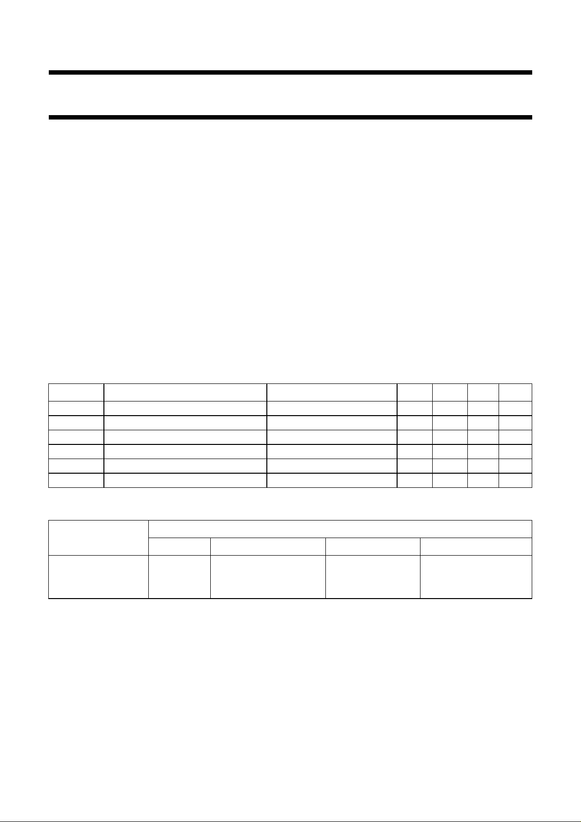
handbook, full pagewidth
SREF
V
SS
LSI1
LSI2
LSE
3
1
4
5
6
V
SUP
2
SUPPLY
PRE-
AMPLIFIER
BB
8
ENABLE
CIRCUIT
START-
CIRCUIT
POWER
AMPLIFIER
TEA1083
MGR045
TEA1083; TEA1083A
7
QLS
handbook, full pagewidth
SREF
PD
V
SS
LSI1
LSI2
LSE
Fig.1 Block diagram (TEA1083).
V
3
12
1
8
9
13
3, 5, 6, 7,
10, 11, 14
n.c.
SUP
2
SUPPLY
PD
PRE-
AMPLIFIER
BB
16
ENABLE
CIRCUIT
START-
CIRCUIT
POWER
AMPLIFIER
TEA1083A
TEA1083AT
15
MGR046
QLS
Fig.2 Block diagram (TEA1083A/AT).
March 1994 3
Philips Semiconductors Product specification
Call progress monitor for line powered
telephone sets
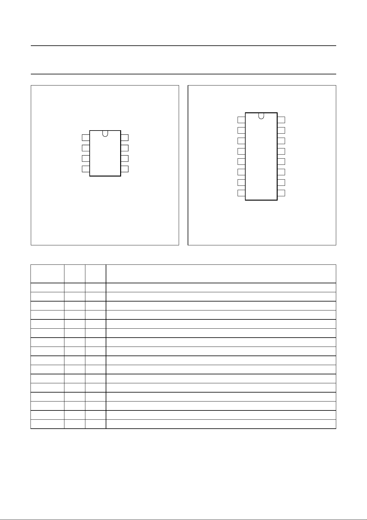
handbook, halfpage
V
SS
SREF
LSI1
1
2
3
4
TEA1083
MGR047
V
8
BB
QLSSUP
7
LSE
6
LSI2
5
Fig.3 Pin configuration (TEA1083).
handbook, halfpage
Fig.4 Pin configuration (TEA1083A/AT).
V
SS
SUP
n.c.
SREF
n.c.
n.c.
n.c.
LSI1
TEA1083; TEA1083A
1
2
3
4
TEA1083A
TEA1083AT
5
6
7
8
MGR048
V
16
BB
15
QLS
14
n.c.
13
LSE
12
PD
11
n.c.
10
n.c.
9
LSI2
PINNING
SYMBOL
V
SS
PIN
DIL16
PIN
DIL8
1 1 negative supply terminal
SUP 2 2 positive supply terminal
n.c. 3 − not connected
SREF 4 3 supply reference input
n.c. 5 − not connected
n.c. 6 − not connected
n.c. 7 − not connected
LSI1 8 4 loudspeaker amplifier input 1
LSI2 9 5 loudspeaker amplifier input 2
n.c. 10 − not connected
n.c. 11 − not connected
PD 12 − power-down input
LSE 13 6 loudspeaker enable input
n.c. 14 − not connected
QLS 15 7 loudspeaker amplifier output
V
BB
16 8 stabilized supply voltage
DESCRIPTION
March 1994 4
Philips Semiconductors Product specification
Call progress monitor for line powered
TEA1083; TEA1083A
telephone sets
Table 1 Comparison of the TEA108X family.
PRODUCT CONDITIONS TEA1083 TEA1083A TEA1085/85A
Application area note 1 call progress monitoring listening-in
PD facility − XX
MUTE or LSE facility note 2 X X X
Dynamic limiter −− X
Howling limiter −− X
V
setting −− X
BB
SEL note 3 X X X
BTL note 3 −− X
Number of pins note 4 8 16 24
Notes
1. A call progress monitor is recommended by the
European Telecommunications Standards Institute
(ETSI) for telephone sets with automatic on-hook
dialling facilities so that audible, or visual, progress of
a call attempt can be monitored. In accordance with
the ETSI (at a frequency of 440 Hz and a line level of
20 dBm (600 Ω)), a minimum level of 50 dBA shall be
guaranteed at a distance of 50 cm from the set. This
corresponds to a minimum level of approximately
100 mV (RMS) (PO≥ 0.2 mW) across a loudspeaker;
Philips type AD2071/Z50.
A listening-in set has to offer the user more facilities
e.g. howling limiting to reduce annoying loudspeaker
and line signals. Dynamic limiting of the loudspeaker
signal, with respect to supply conditions, can also be
required. Acoustic output levels for listening-in sets are
approximately 70 to 75 dBA. This corresponds to a
loudspeaker level of approximately 1 mV (RMS)
(PO≈ 20 mW).
2. The MUTE function of the TEA1085A has a logic input;
the MUTE function of the TEA1085 has a toggle input.
3. SEL: loudspeaker connected in a single-ended-load
configuration
BTL: loudspeaker connected in a bridge-tied-load
configuration
4. Consult the product specification for the package
outline/s.
FUNCTIONAL DESCRIPTION
The TEA1083/83A is normally used in conjunction with a
transmission circuit of the TEA1060 family. The circuit
must be connected between the positive line terminal
(pin 2) and pin SLPE of the transmission IC. The
transmission characteristics (impedance, gain settings,
etc.) are not affected.
An interconnection between the TEA1083/83A and a
member of the TEA1060 family is illustrated in Fig.5.
Supplies SUP, SREF, V
BB
and V
SS
In Fig.6 the line current is divided into ITR for the
transmission IC and I
for the monitoring circuit
SUP
TEA1083/83A.
ITR is constant:
ITR=V
I
SUP=Iline
/ R20
int
− ICC− I
TR
Where:
• V
is an internal temperature compensated reference
int
voltage of 500 mV (typ) between pins SUP and SREF
• R20 is a resistor connected between SUP and SREF
• ICC is the internal current consumption of the TEA106X
(approximately 1 mA).
A practical value for resistor R20 is 150 Ω; this produces a
current of approximately 3.3 mA (typ) for ITR and I
approximately equal to I
− 4.3 mA.
line
SUP
is
March 1994 5

Philips Semiconductors Product specification
Call progress monitor for line powered
telephone sets
The circuit stabilizes its own supply voltage at VBB.
Transistor TR1 provides the supplies for the internal
circuits. Transistor TR2 is used to minimize signal
distortion on the line by momentarily diverting the input
current to VSS whenever the instantaneous value of the
voltage at V
fixed to a typical value of 2.95 V.
The supply at VBB is decoupled with respect to VSS by a
220 µF capacitor (C20).
The DC voltage (V
transmission IC and V
V
− VSS = V
SUP
The reference voltage of the transmission IC has to be
adjusted to a level where V
400 mV. The minimum voltage space between SUP and
VBB (400 mV) is required to maintain a 'high' efficiency of
the internal supply for mean speech levels. V
specified maximum level.
The internal current consumption of the TEA1083/83A
(I
) is typically 2.5 mA (where V
SUP0
The current I
0.4 mA) for the circuitry connected to SUP and I
(approximately 2.1 mA) for the internal circuitry connected
to VBB(see Fig.6).
LOUDSPEAKER AMPLIFIER (LSI1/LSI2 and QLS)
The TEA1083/83A has symmetrical inputs at LSI1 and
LSI2. The input signal is normally taken from the earpiece
output of the transmission circuit (see Fig.5) and/or from
the signal output of the DTMF generator via a resistive
attenuator.
The attenuation factor must be chosen in accordance with
the output levels from the transmission IC and/or DTMF
generator and, in accordance with the required output
power and permitted signal distortion from the
loudspeaker signal.
The output QLS drives the loudspeaker as a single-ended
load. The output stage has been optimized for use with a
50 Ω loudspeaker (e.g. Philips type AD2071). The
loudspeaker amplifier is enabled when the LSE input goes
HIGH. The gain of the amplifier is fixed at 35 dB.
Volume control of the loudspeaker signal can be obtained
by using a level control at the input (see Fig.5).
drops below the supply voltage VBB. VBB is
SUP
− VSS) is determined by the
SUP
; thus
int
+ V
LN−SLPE
consists of currents I
SUP0
int
SUP
.
− V
SUP
is greater than
BB (max)
BB (max)
− VSS= 3.6 V).
(approximately
BIAS
BB0
is the
TEA1083; TEA1083A
The maximum voltage swing at the QLS output is
V
V
I
available voltage space (VBB). Higher input levels and/or
lower supply currents will result in an increase of the
harmonic distortion due to signal clipping.
With a limit of 2.5 V (p-p), the maximum output swing is
dependent on the supply current and loudspeaker
impedance. It can be approximated, for low distortions, by
the following equation:
V
Where;
• V
• RLS= the loudspeaker impedance
• I
POWER-DOWN INPUT (PD)
During pulse dialling or register recall (timed loop break)
the telephone line is interrupted, thereby breaking the
supply current to the transmission IC. The capacitor
connected to V
TEA1083/83A during the supply breaks.
By making the PD input HIGH during the loop break, the
requirement on the capacitor is eased and, consequently,
the internal current consumption I
reduced from 2.1 mA to 400 µA typically. Transistors TR1
and TR2 are inhibited during power-down and the bias
current is reduced from approximately 400 µA to
approximately 50 µA with V
equation:
I
Where 3.6 < V
2Vd is the voltage drop across 2 internal diodes
(approximately 1.3 V)
Ra is an internal resistor (typical 50 kΩ)
LOUDSPEAKER ENABLE INPUT (LSE)
The LSE input has a pull-down structure. It switches the
loudspeaker amplifier, in the monitoring condition, by
applying a HIGH level at the input. The amplifier is in the
standby condition when LSE is LOW (input open-circuit or
connected to V
= 2.5 V (typical with 50 Ω load). The input level
O(p-p)
is approximately 16 mV(rms) and the supply current
LSI
> 11 mA. In this condition the signal is limited by the
SUP
O(p-p)
O(p-p)
SUPO
SUP(PD)
=2×(I
= the peak-to-peak level of the loudspeaker
= 2.5 mA (typ.)
= I
BIAS(PD)
− I
SUP
provides the supply for the
BB
= (V
< VBB+ 3V
SUP
).
SS
) ×π×R
SUPO
SUP
− 2Vd)/Ra
SUP
LS
(see Fig.5) is
BB0
= 3.6 V in the following
March 1994 6
 Loading...