

Philips TEA1081T-C2, TEA1081-C2 Datasheet

DATA SH EET
Product specification
Supersedes data of February 1988
File under Integrated Circuits, IC03
September 1994
INTEGRATED CIRCUITS
Philips Semiconductors
TEA1081
Supply circuit with power-down for
telephone set peripherals
September 1994 2
Philips Semiconductors Product specification
Supply circuit with power-down for
telephone set peripherals
TEA1081
FEATURES
• High input impedance for audio signals
• Low DC series resistance
• High output current
• Large audio signal handling capability
• Low distortion
• Two modes of operation:
– output voltage that follows the DC line voltage
– regulated output voltage
• Power-down input
• Low number of external components.
GENERAL DESCRIPTION
The TEA1081 is an integrated circuit for use in
line-powered telephone sets to supply peripheral circuits
for extended dialling and/or loudspeaker facilities.
The IC uses a part of the surplus line current normally
drawn by the voltage regulator of the speech/transmission
circuit. A power-down function isolates the IC from its load
and reduces the input current.
QUICK REFERENCE DATA
ORDERING INFORMATION
SYMBOL PARAMETER CONDITIONS MIN. TYP. MAX. UNIT
V
LN
operating DC line voltage 2.5 − 12.0 V
V
O
DC output voltage 2.0 − 10.0 V
∆V
LN-O
voltage drop from line to output IO=0mA − 0.5 − V
R
S
internal series resistance − 20 −Ω
I
O
output current (pin 7) VLN=4V
TEA1081 −−30 mA
TEA1081T −−20 mA
V
LN(rms)
AC line voltage (RMS value) VLN=4V; IO=15mA;
THD=2%
− 1.5 − V
I
INT
internal supply current VLN=4V; IO= 0 mA;
PD = LOW; VSP= V
O
− 0.8 1.4 mA
T
amb
operating ambient temperature −25 − +70 °C
TYPE NUMBER
PACKAGE
NAME DESCRIPTION VERSION
TEA1081 DIP8 plastic dual in-line package; 8 leads (300 mil) SOT97-1
TEA1081T SO8 plastic small outline package; 8 leads; body width 3.9 mm SOT96-1
September 1994 3
Philips Semiconductors Product specification
Supply circuit with power-down for
telephone set peripherals
TEA1081
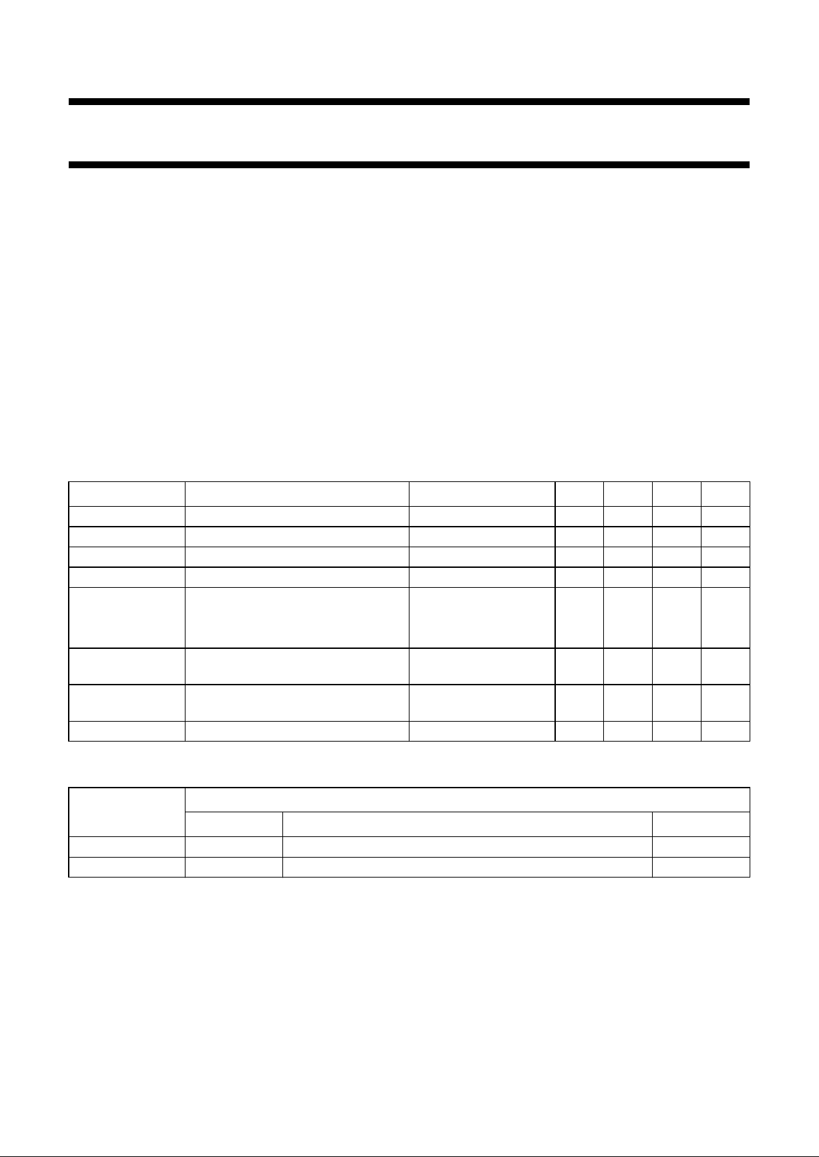
BLOCK DIAGRAM
Fig.1 Block diagram.
handbook, full pagewidth
MLC166
A2
A1
A3
1/2 V
O
POWER-
DOWN
REFERENCE
CURRENT
8
4
6
SP
PD
VA
7
QS
TR2
TR1
0.5 V
R
S
1
LN
5
IF
3
AD
2
VN
TEA1081
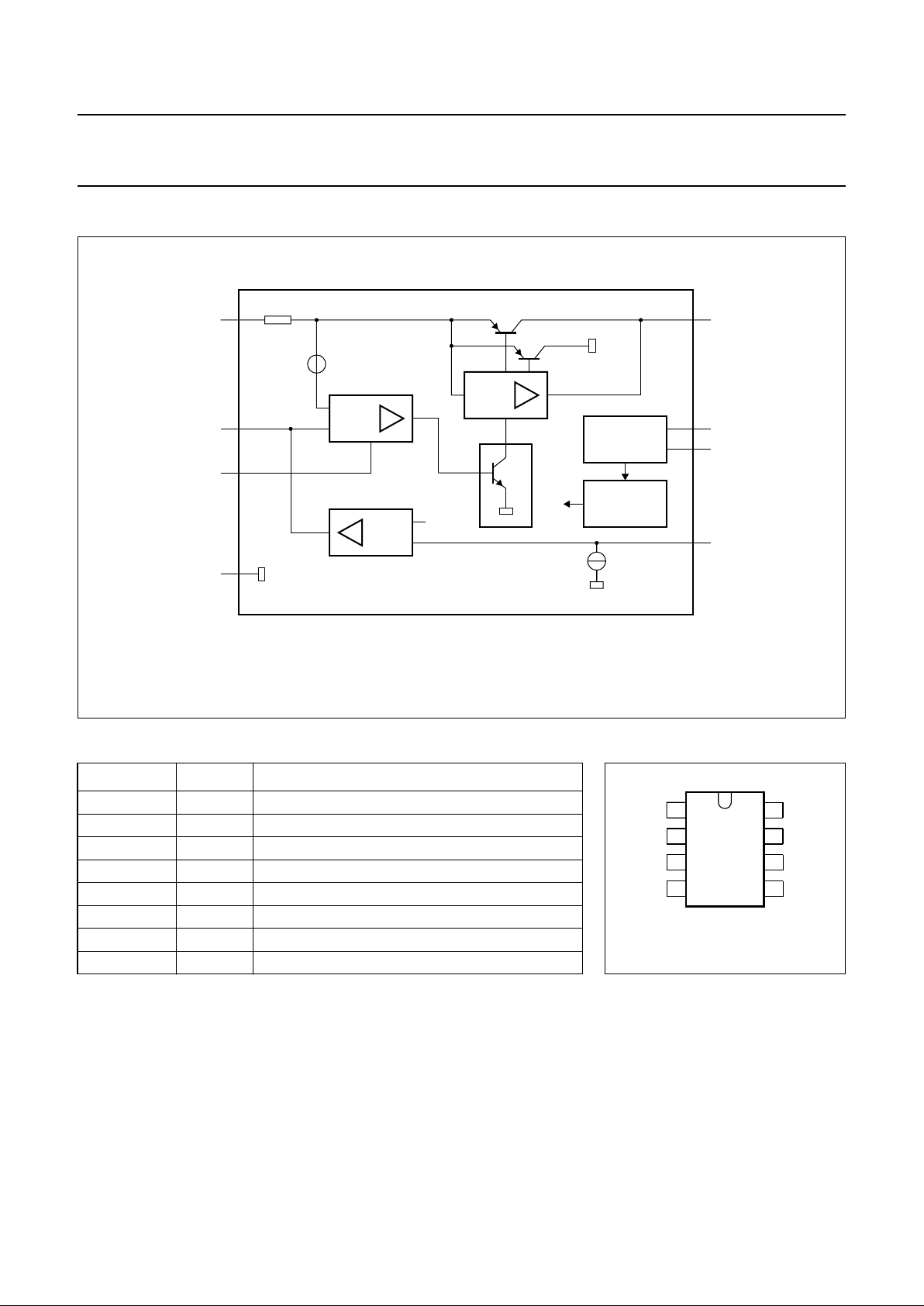
PINNING
SYMBOL PIN DESCRIPTION
LN 1 positive line terminal
VN 2 negative line terminal
AD 3 amplifier decoupling
PD 4 power-down input
IF 5 low-pass filter input
VA 6 output voltage adjustment
QS 7 power supply output
SP 8 supply input; power-down circuit
Fig.2 Pin configuration.
age
1
2
3
4
8
7
6
5
SP
QS
VA
IF
LN
VN
AD
PD
TEA1081
MLC167
September 1994 4
Philips Semiconductors Product specification
Supply circuit with power-down for
telephone set peripherals
TEA1081
FUNCTIONAL DESCRIPTION
The TEA1081 is a supply interface between telephone line
and peripheral devices in the telephone set. The high input
impedance of the circuit allows direct connection to the
telephone line (via a diode bridge). An inductor function is
obtained by amplifier A1, resistor RS (see Fig.1) and an
external low-pass RC filter.
Under the control of amplifier A2, transistor TR1 supplies
peripheral devices and transistor TR2 minimizes line
signal distortion by momentarily diverting input current to
ground whenever the instantaneous value of the line
voltage drops below the output voltage.
Internal circuits are biased by a temperature and line
voltage compensated reference current source.
The power-down circuit isolates the supply circuit from
external circuitry.
Line terminals: LN and VN (pins 1 and 2)
The input terminals LN and VN can be connected directly
to the line. The minimum DC line voltage required at the
input is expressed by formula (1); see also Table 1.
(1)
Table 1 Explanation of formula (1).
The internal current (I
INT
) at IO = 0 mA is typically 0.8 mA
at VLN = 4 V and reaches a maximum of 1.4 mA at
VLN=12V.
Supply terminals: QS and VA (pins 7 and 6)
Peripheral devices are supplied from QS (pin 7). Two
modes of output voltage regulation are available.
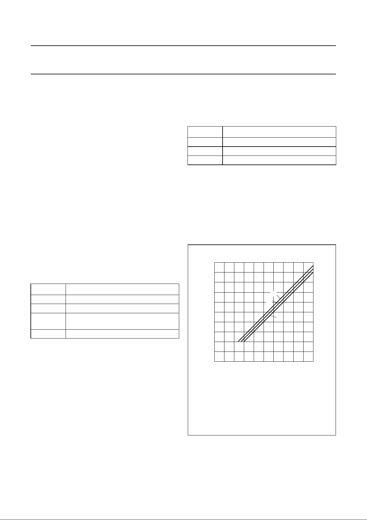
OUTPUT VOLTAGE FOLLOWS LINE VOLTAGE (SEE FIG.3)
The TEA1081 operates in this mode when there is no
external resistor (RV) between QS and VA (see Fig.6).
SYMBOL DESCRIPTION
I
1
input current
R
S
internal series resistance
V
LNmin
minimum instantaneous line voltage
(1.4 V at IO = 5 mA)
V
LN(P)
required peak level of AC line voltage
V
LNI1RS
× V
LNminVLN P()
V()++=
The output voltage follows the line voltage and is
expressed by formula (2); see also Table 2.
(2)
Table 2 Explanation of formula (2).
R
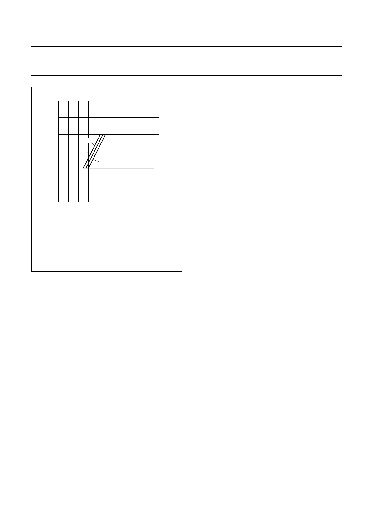
EGULATED OUTPUT VOLTAGE (SEE FIG.4)
The circuit operates in this mode when an external resistor
(RV) is connected between QS and VA (see Fig.6).
The output voltage is held constant at VO = 2 × I6× RV (V)
as soon as the line voltage
VLN>(2×I6×RV+I1×RS+ 0.5) (V)
The control current I6 is typically 20 µA.
SYMBOL DESCRIPTION
V
LN
line voltage
I
1
input current
R
S
internal series resistance
V
O
V
LNI1RS
0.5+×()– V()=
Fig.3 Output voltage as a function of line voltage.
Application without RV.
(1) I1 = 5 mA.
(2) I1 = 20 mA.
(3) I1 = 30 mA; not valid for TEA1081T.
handbook, halfpage
010
10
0
2
MLC168
4
6
8
2468
V
O
(V)
V (V)
LN
(1)
(2)
(3)
September 1994 5
Philips Semiconductors Product specification
Supply circuit with power-down for
telephone set peripherals
TEA1081
Input and output currents I1 and IO (pins 1 and 7)
The maximum available current into pin 1 (I
1
) is
determined by:
• The minimum line current (I
LINEmin
) that is available for
the telephone set
• The specified minimum input current (I
LNmin
) for the
speech/transmission circuit.
That is I
1max
= I
LINEmin
− I
LNmin
.
At V
LN(rms)
< 150 mV, the input current I1is approximately:
I1=I
INT
+k×IO (mA)
Where:
I
INT
= internal supply current (0.8 mA at VLN= 4 V);
k = correction factor (k < 1.1 for the specified output
current range).
With large line signals the instantaneous line voltage may
drop below VO+ 0.4 V. Normally (when VLN>VO+ 0.4 V),
instantaneous current flows from LN to QS (pin 1 to pin 7)
to the output load.
When VLN<VO+ 0.4 V, the instantaneous current is
diverted to pin 2 to prevent distortion of the line signal.
Fig.4 Output voltage as a function of line voltage.
RV connected between QS and VA.
(1) I1 = 5 mA.
(2) I1 = 20 mA.
(3) I1 = 30 mA; not valid for TEA1081T.
handbook, halfpage
0
6
4
2
0
210
MLC169
468
(1)
(2)
(3)
V
O
(V)
V (V)
LN
V
R = 100 kΩ
75 kΩ
50 kΩ
Input current at V
LN(rms)
= 1 V and without R
V
approximates to:
I1 = I
INT
+2×IO (mA)
The maximum supply current (within the specified output
current limits) available for peripheral devices is shown by:
I
Omax
=
Where:
I
LINEmin
is the minimum line current of the telephone set;
I
LNmin
is the specified minimum input current of the
speech/transmission circuit.
Input low-pass filter: IF (pin 5)
The input impedance between LN and VN at audio
frequencies is determined by the filter elements C
L
(between pins 1 and 5), RL (between pins 5 and 7) and the
internal resistor RS(typical value 20 Ω).
At audio frequencies the TEA1081 behaves as an inductor
of the value LI= CL× RL× RS (H). The typical value of LI at
CL = 2.2 µF and RL = 100 kΩ is 4.4 H.
Amplifier decoupling: AD (pin 3)
To ensure stability, a 68 pF decoupling capacitor is
required between AD (pin 3) and LN (pin 1).
If I
Omin
< 1.5 mA, a 47 pF capacitor has to be added
between AD (pin 3) and VA (pin 6).
Power-down inputs: PD and SP (pins 4 and 8)
During pulse dialling or register recall, or if the input current
to pin 1 is insufficient to maintain the output current, the
supply to peripheral devices can be switched off by
activating the PD input at pin 4. With PD = HIGH, the input
current is reduced to 40 µA (typ.) at V
LN
= 4 V and the
internal circuits are isolated from the load at QS (pin 7).
The power-down circuit is supplied via the SP input (pin 8).
SP can be wired to QS in conditions where VO>V
SPmin
during line interruptions. When VO<V
SPmin
, SP should be
wired to an external supply point (e.g. to VCC of the
TEA1060 family circuit).
When power-down is not required, the PD and SP inputs
can be left open-circuit.
I
LINEminILNmin
– I
INT
–
2
-----------------------------------------------------------
 Loading...