

Page 1

Colour Television Chassis
TE1.1E
AA
Contents Page
1. Technical Specifications, Connections and Chassis
Overview 2
2. Safety & Maintenance Instructions, Warnings and
Notes 3
3. Directions for Use 5
4. Mechanical Instructions 7
5. Service Modes, Error Codes and Faultfinding 8
6. Block Diagram, I2C Diagram and
Supply Voltage Diagram
Block Diagram 11
2
I
C Diagram 12
Supply Voltage Diagram 13
7. Electrical Diagrams and PWB’s Diagram CBA
Main Panel: (Diagram A) 14-17 18-19
Main Panel: 2W Version (Diagram A) 20-23 24-25
CRT Panel (Diagram B) 26 26
8. Alignments 27
9. Circuit Description (Not Applicable) 30
Abbreviation List 30
IC Data Sheets 31
10 Spare Parts List 52
11 Revision List 57
CL 36532010_000.eps
200203
©
Copyright 2003 Philips Consumer Electronics B.V. Eindhoven, The Netherlands.
All rights reserved. No part of this publication may be reproduced, stored in a
retrieval system or transmitted, in any form or by any means, electronic,
mechanical, photocopying, or otherwise without the prior permission of Philips.
Published by LM 0370 Service PaCE Printed in the Netherlands Subject to modification EN 3122 785 13542
Page 2
EN 2 TE1.1E1.
Technical Specifications, Connections, and Chassis Overview
1. Technical Specifications, Connections, and Chassis Overview
1.1 Technical Specifications
1.1.1 Reception
Tuning system : PLL
Colour systems : PAL
: SECAM
Sound system : Mono
A/V Connections : Scart
: Headphone front
Channel selection : Air
: Cable
IF Frequency : B/G, D/K, L: 38.9 MHz
: L’: 33.4 MHz
: I: 39.5 MHz
Aerial input : 75 Ohm
1.1.2 Miscellaneous
Audio Output (RMS) : 1 x 1 W
Mains Voltage : 150/240 V (± 10 %)
Mains Frequency : 50 Hz (± 5 %)
Power Consumption : 45 W
Standby Power Consumption : 4 W
1.2 Connection/Control Facilities
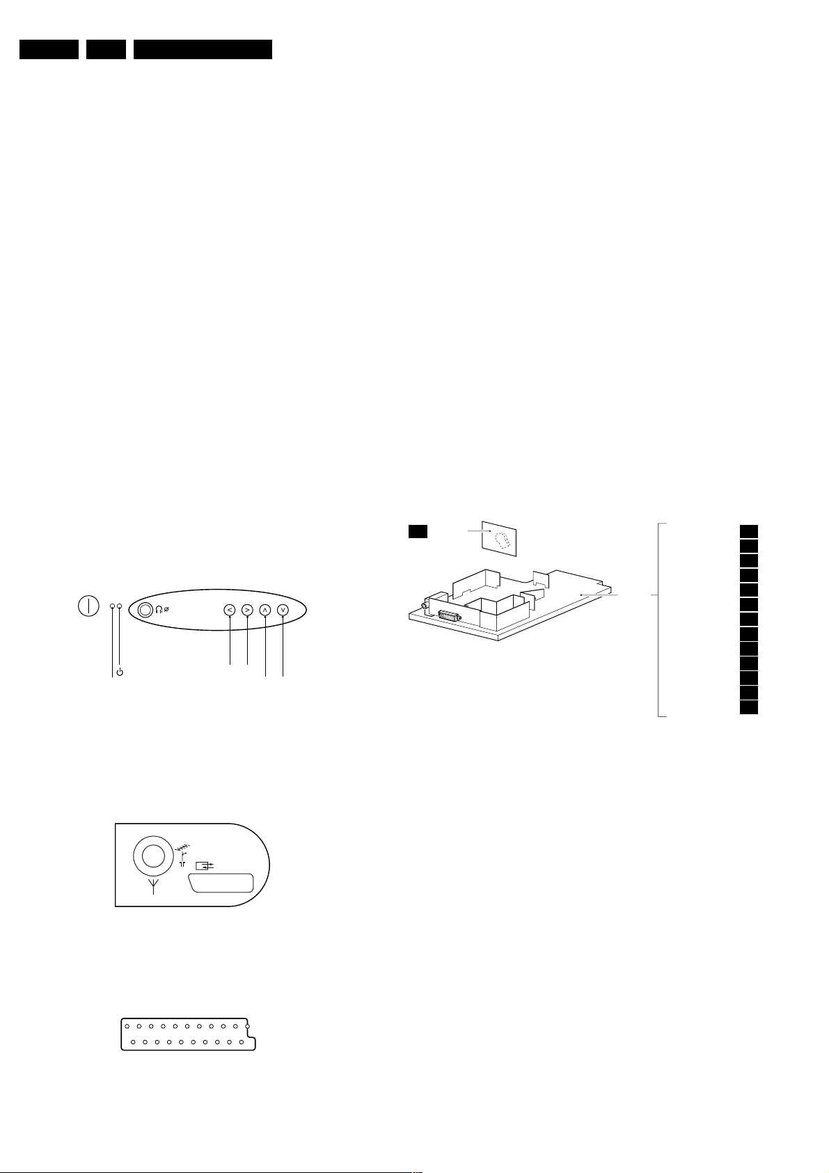
1.2.1 TV Front Control
FRONT CONTROL
3.5
- VOLUME +
IR
Receiver
Figure 1-1 Front control
1.2.2 TV Rear Connections
- PROGRAM +
CL 36532010_017.eps
250203
1 - Audio - R 0.5 Vrms / 1 kOhm k
2 - Audio - R 0.5 Vrms / 10 kOhm j
3 - Audio - L 0.5 Vrms / 1 kOhm k
4 - Audio Ground H
5 - Blue Ground H
6 - Audio - L 0.5 Vrms / 10 kOhm j
7 - Blue 0.7 Vpp / 75 Ohm j
8 - CVBS-status 0 - 1.3 V: INT
4.5 - 7 V: EXT 16:9
9.5 - 12 V: EXT 4:3
9 - Green Ground H
10 -
11 - Green 0.7 Vpp / 75 Ohm j
12 -
13 - Red Ground H
14 - CVBS status Ground H
15 - Red 0.7 Vpp / 75 Ohm j
16 - RGB status 0 - 0.4 V: INT
1 - 3 V: EXT / 75 Ohm j
17 - CVBS Ground H
18 - RGB status Ground H
19 - CVBS-out 1 Vpp / 75 Ohm k
20 - CVBS-in 1 Vpp / 75 Ohm j
21 - Shielding Ground H
1.3 Chassis Overview
CRT BOARD
B
MAIN
CHASSIS
PANEL
Figure 1-4 PWB location
µ-CONTROLLER +
VIDEO PROCESSOR
FRONT AV
SCARTS
POWER SUPPLY
VERTICAL
HORIZONTAL
TUNER
HEADPHONE
EEPROM
RESET
INFRARED + LED +
KB MODULE
MONO AUDIO AMPLIFIER
SECAM L/L' MONO
CL 36532010_018.eps
A1
A2
A3
A4
A5
A6
A7
A8
A9
A10
A11
A12
A13
200203
Euro AV
REAR CONNECTIONS
EURO-AV
CL 36532010_021.eps
250203
Figure 1-2 Rear connections
121
CL96532137_056.eps
202
171199
Figure 1-3 SCART connector
Page 3
Safety & Maintenance Instructions, Warnings, and Notes
2. Safety & Maintenance Instructions, Warnings, and Notes
EN 3TE1.1E 2.
Index of this chapter:
1. Safety Instructions for Repairs
2. Maintenance Instructions
3. Warnings
4. Notes
2.1 Safety Instructions for Repairs
Safety regulations require that during a repair:
• Due to the "hot" parts of this chassis, the set must be
connected to the AC power via an isolation transformer.
• Safety components, indicated by the symbol h, should be
replaced by components identical to the original ones.
• When replacing the CRT, safety goggles must be worn.
Safety regulations require that after a repair, the set must be
returned in its original condition. Pay particular attention to the
following points:
• General repair instruction: as a strict precaution, we advise
you to resolder the solder connections through which the
horizontal deflection current is flowing, in particular:
– all pins of the line output transformer (LOT)
– fly-back capacitor(s)
– S-correction capacitor(s)
– line output transistor
– pins of the connector with wires to the deflection coil
– other components through which the deflection current
flows.
Note: This resoldering is advised to prevent bad connections
due to metal fatigue in solder connections and is therefore only
necessary for television sets more than two years old.
• Route the wire trees and EHT cable correctly and secure
them with the mounted cable clamps.
• Check the insulation of the AC power cord for external
damage.
• Check the strain relief of the AC power cord for proper
function, to prevent the cord from touching the CRT, hot
components, or heat sinks.
• Check the electrical DC resistance between the AC plug
and the secondary side (only for sets that have an isolated
power supply). Do this as follows:
1. Unplug the AC power cord and connect a wire between
the two pins of the AC plug.
2. Turn on the main power switch (keep the AC power
cord unplugged!).
3. Measure the resistance value between the pins of the
AC plug and the metal shielding of the tuner or the
aerial connection of the set. The reading should be
between 4.5 MOhm and 12 MOhm.
4. Switch the TV "off" and remove the wire between the
two pins of the AC plug.
• Check the cabinet for defects, to prevent the possibility of
the customer touching any internal parts.
2.2 Maintenance Instructions
It is recommended to have a maintenance inspection carried
out by qualified service personnel. The interval depends on the
usage conditions:
• When the set is used under normal circumstances, for
example in a living room, the recommended interval is
three to five years.
• When the set is used in an environment with higher dust,
grease or moisture levels, for example in a kitchen, the
recommended interval is one year.
• The maintenance inspection includes the following actions:
1. Perform the "general repair instruction" noted above.
2. Clean the power supply and deflection circuitry on the
chassis.
3. Clean the picture tube panel and the neck of the picture
tube.
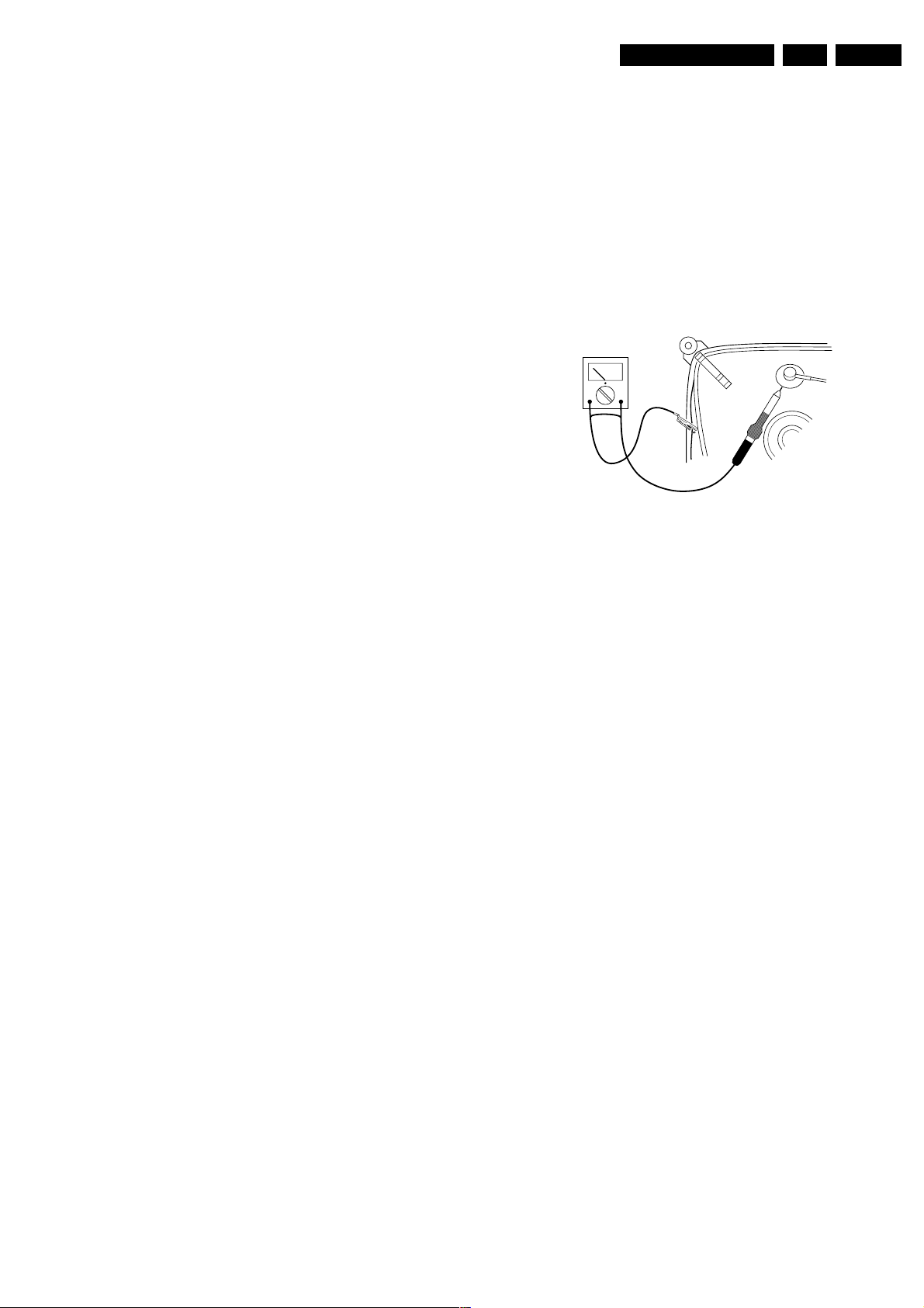
2.3 Warnings
• In order to prevent damage to ICs and transistors, avoid all
high voltage flashovers. In order to prevent damage to the
picture tube, use the method shown in Fig. 2-1, to
discharge the picture tube. Use a high voltage probe and a
multi-meter (position Vdc). Discharge until the meter
reading is 0 V (after approx. 30 s).
V
CL96532156_040.eps
Figure 2-1 Discharge picture tube
• All ICs and many other semiconductors are susceptible to
electrostatic discharges (ESD w). Careless handling
during repair can reduce life drastically. When repairing,
make sure that you are connected with the same potential
as the mass of the set by a wristband with resistance. Keep
components and tools also at this potential.
• Available ESD protection equipment:
– Complete kit ESD3 (small tablemat, wristband,
connection box, extension cable, and ground cable)
4822 310 10671.
– Wristband tester 4822 344 13999.
• Together with the deflection unit and any multi-pole unit,
flat square picture tubes form an integrated unit. The
deflection and the multi-pole units are set optimally at the
factory. Adjustment of this unit during repair is therefore not
recommended.
• Be careful during measurements in the high voltage
section and on the picture tube.
• Never replace modules or other components while the unit
is switched "on".
• When you align the set, use plastic rather than metal tools.
This will prevent any short circuits and the danger of a
circuit becoming unstable.
2.4 Notes
2.4.1 General
• Measure the voltages and waveforms with regard to the
chassis (= tuner) ground (H), or hot ground (I), depending
on the area of circuitry being tested.
• The voltages and waveforms shown in the diagrams are
indicative. Measure them in the Service Default Mode (see
“Service Modes, Error Codes, and Faultfinding” section)
with a color bar signal and stereo sound (L: 3 kHz, R: 1 kHz
unless stated otherwise) and picture carrier at 61.25 MHz
(NTSC, channel 3).
• Where necessary, measure the waveforms and voltages
with (D) and without (E) aerial signal. Measure the
voltages in the power supply section both in normal
operation (G) and in standby (F). These values are
indicated by means of the appropriate symbols.
140501
Page 4

EN 4 TE1.1E2.
• The picture tube panel has printed spark gaps. Each spark
gap is connected between an electrode of the picture tube
and the Aquadag coating.
• The semiconductors indicated in the circuit diagram and in
the parts lists are completely interchangeable per position
with the semiconductors in the unit, irrespective of the type
indication on these semiconductors.
2.4.2 Schematic Notes
• All Resistor values are in ohms and the value multiplier is
often used to indicate the decimal point location (e.g. 2K2
indicates 2.2 kOhm).
• Resistor values with no multiplier may be indicated with
either an "E" or an "R" (e.g. 220E or 220R indicates 220
Ohm).
• All Capacitor values are expressed in Micro-Farads (µ =
-6
x10
), Nano-Farads (n = x10-9), or Pico-Farads (p = x10
12
).
• Capacitor values may also use the value multiplier as the
decimal point indication (e.g. 2p2 indicates 2.2 pF).
• An "asterisk" (*) indicates component usage varies. Refer
to the diversity tables for the correct values.
• The correct component values are listed in the Electrical
Replacement Parts List. Therefore, always check this list
when there is any doubt.
Safety & Maintenance Instructions, Warnings, and Notes
-
2.4.3 Practical Service Precautions
• It makes sense to avoid exposure to electrical shock.
While some sources are expected to have a possible
dangerous impact, others of quite high potential are of
limited current and are sometimes held in less regard.
• Always respect voltages. While some may not be
dangerous in themselves, they can cause unexpected
reactions - reactions that are best avoided. Before reaching
into a powered TV set, it is best to test the high voltage
insulation. It is easy to do, and is a good service precaution.
• Before powering up the TV set with the back cover off
(or on a test fixture), attach a clip lead to the CRT DAG
ground and to a screwdriver blade that has a well insulated
handle. After the TV is powered on and high voltage has
developed, probe the anode lead with the blade, starting at
the case of the High Voltage Transformer (flyback - IFT).
Move the blade to within two inches of the connector of the
CRT. If there is an arc, you found it the easy way,
without getting a shock! If there is an arc to the
screwdriver blade, replace the part which is causing the
problem; the High Voltage Transformer or the lead (if it is
removable).
Page 5
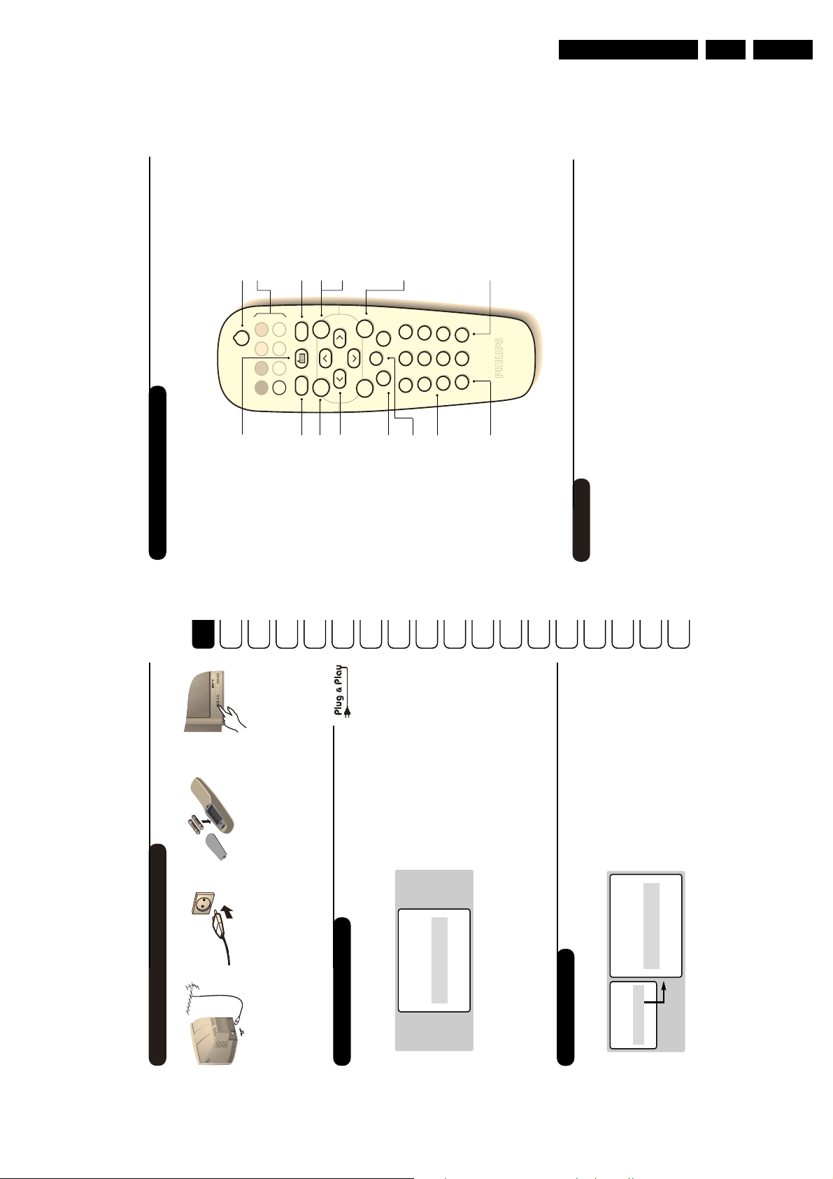
3. Directions for Use
SMART RADIO SMART
.
ª-
MENU
[
”
P
-
+
-
+
123
4
56
789
0
`
Ø
Ë
ŸÓ›
¤
Rich,Natural,Soft,
Directions for Use
EN 5TE1.1E 3.
Remote control keys
Teletext keys (teletext version *)
Pre-set image
standb y.To turn on the TV,press
Standby
Lets you place the TV se t on
P @ #,b,0 to 9.
programme.
or
Á Previous programme
To access the previously view ed
FR
Pre-set sound (only available on
NL
* D epending on the model,there are 2 different ve rsions of the rem o te co ntro l.
 key not used (teletext version *)
GB
Used to acce ss a series of stored
certain versions)
settings:
Used to access a se ries of stored
DE
Multimedia and return to Personal.
Menu
Voice,Music,Theatre.
settings:
IT
c Teletext call (teletext version*)ord Screen information
Cursor / Format 16:9
To call up or exit the menus.
These 4 keys are used to navigate
DK
disp lay of the num ber.
sec o nds to activate perm anent
sleeptimer.Pre ss the key for 5
num berand time rem aining for the
To display / clear the pro gram
Volume
îÏ keys
the picture vertically.
To adjust the sound level
are used to enlarge or com press
through the menus.The
NO
For some programs, the title of the
Program selection
To access the next or previous
programme.The num ber is
disp layed for a few moments.
Mute
Number keys
To mute or re store the sound.
SF
SU
program will be displayed at the
Direc t acce ss to the programmes.
For a 2 digit program ,enter the 2nd
#
con nected equipm ent.
Selection of EXT socket
Press seve ral times to select the
bottom of the screen.
Sleep
a preset time (fro m 0 to 240
digit before the dash disapp e ars.
To select an autom atic standby after
ES
RU
minutes).
PT
GR
Direct access to the items
(only available on certain versions)
Teletext
Teletext call
TR
HU
s to stop /resum e the sequence.
x seve ral time to enlarge the p age.
d to return to the co ntents page (usually page 100).
Press
item s or corresponding pages.
screen.The 4 coloured keys are used to access the
Coloured areas are displayed at the bottom of the
c key to call teletext,change to transparent
item s that can be accessed.
mode and then exit.The summary appears with a list of
Press the
PL
Contents
If the channel selected does not broadcast teletext, the
screen remain black.
CZ
Press
Enlarge a page
0 to
Enter the num ber of the page required using the
9 or@ P # keys (always 3 digits).T he num ber is
Selecting a page
SK
autom atically.Press
Certain p ages contain sub-pages which follow on
Stop sub-page acquisition
If the counter continues searching, the page is not transmitted.
disp layed.Repeat this operation to view another page.
disp layed top left,the counter turns and then the page is
y to display or hide the co nce aled inform ation.
Press
Hidden information (gam es solutions)
4
3
.
Ȭ
H
d.
standb y m od e ,p ress P
television re m ains in
the on/off key.If the
To sw itch on the set,p ress
on the re m o te co ntro l.
Ï key to select Program No
programme is found, see Tips chapter at the
09 or@P# keys to select the
program s found. A t the end of the search ,the
menu disap p ears.
pro gress of the se arch and the num ber of
TV programmes will be stored.This operation
If your country does not appear in the list, select
way round.
that they are the right
(supplied) making sure
type batteries
Insert the two R6-
takes a few minutes.The disp lay sho w s the
choice “. . .”
é The se arc h starts autom atically.All the available
To exit or interrupt the search, press
If no
end of the instruction for use.
See Program so r t below .
ren u m b e r these programmes as yo u wish.
num ber 99,98,97,… etc.You may now
“ The programmes found are arranged by
program yo u wish to renu m b e r.
“ Use the
Ï key,select Store and pre ss ¬.
and enter the new num ber with the
keys.
wish to renum b er.
‘ Then use the
è To quit the m en us,press
( With the
§ Repeat steps “ to ( for each pro gram yo u
Ï.
(220-240 V / 50 Hz).
into a wall so ck et
Insert the mains plug
Country ... ÆAutostore
Ȭ keys on the rem o te contro l to
”- and ”+ keys on the TV set for 5
If the menu is not displayed, press and hold down
prom pts you to select the country:
time,a menu is disp layed on screen.This menu
When yo u turn on the TV set for the first
Installing your television set
æÂê®
the re ar of the set.
into the : soc ke t at
Insert the aerial plug
Quick installation
the
select yo u r country and validate with
seconds to display the menu.
& Use the
the screen.
Program sort
& Pre ss key H.The Main menuis disp layed on
System Europe ÆSearch 224 MHz
Æ
Manual Store
î key,select Manual Store and
¬.
press
é With the
Page 6
EN 6 TE1.1E3.
Directions for Use
Manual store
choice France.
standard ).
* Except for France (LL’standard), you must select
H key.
one at a time.
This menu is used to store the programmes
& Pre ss the
+
5
”
H.
n key.
d.
¬.The se arc h starts.O nce a
0 to 9 keys.
¬.The program is stored.
d.
Ȭ or0 to 9 keys.
programme is found, see Tips chapter at the end
directly using the
required programme,this can be entered
If no
programme is found,the scanning stops.G o to
the next step.If yo u know the frequency of the
‘ Search: p re ss
of the instruction for use.
( Program No.: enter the require d num ber
store.
with the
! To quit the m en us,press
è Repeat steps ‘ to § for each programme to
§ Store: p re ss
• Brightness: this changes picture brilliance .
Sharpness: this change s the picture definition.
betw een the light and dark tones.
Auto Store:to start autom atic search for all
•
• Colour: this chan ges the intensity of the colour.
•
• Contrast: this changes the difference
To quit or interrupt the search, press
ren u m b e r the programmes (see p.3).
yo u need to use the Manual Store menu to
programmes available in yo u r region.Then,
Manual Store:see top of page .
•
“ To quit the m en us,press
keys are used to adjust the volum e level.
+) and PRO G RA M - + (- P +).
”
VO LUM E - + (-
- and
”
+ keys to se lect an d adjust.
”
.
(p. 57)
#
Brightness
Colour
Contrast
Sharpness
Auto Store
Manual Store
To select co nn ected equipm ent,pre ss seve ral times the
fro nt AV co nn ections (when available).
Use the euroco n nector so cket located at the back of the set or the
Connecting peripheral equipment
System Europe ÆSearch 224 MHz
Æ
Ȭ keys to adjust.:
î key,select Manual Store and
¬.U se the îÏ keys to se lect a
press
é With the
Manual Store
setting and the
Europe (autom atic detection*)
îÏ keys to select a setting an d
West Europe (BG stand ard),East Europe
(DK standard),UK (I stand ard) or France (LL’
or
“ System: se lect
Other settings in the menu
Ȭ keys to adjust.:
the
& Pre ss the H key.
é Use the
Brightness!-+
Other functions
”
@
The
The headphone impedance must be between 32 and 600 Ohms.
When headphones are con nected,the sound on the TV set will be cu t.
Most equipment (decoder,VCR) carries out the switching itself.
Headphones socket (only available on certain versions)
The keys on the TV set
see at the end of the booklet
The TV se t has 4 keys :
To access or exit the m en u s,p ress simultaneo usly the
keys.Then use the - P +and -
Tips :
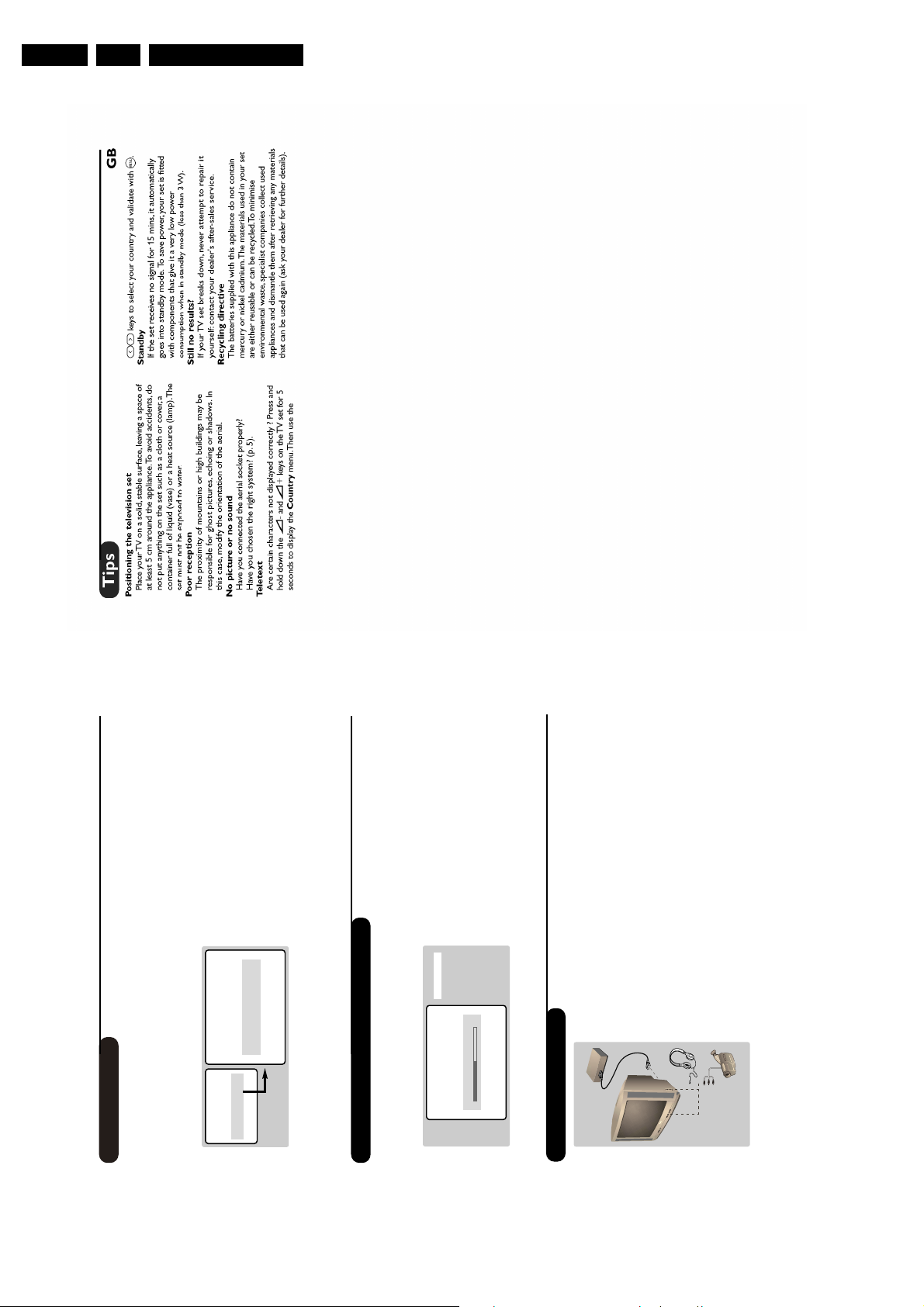
Page 7
4. Mechanical Instructions
Mechanical Instructions
EN 7TE1.1E 4.
Note: Figures below can deviate slightly from the actual
situation, due to the different set executions.
4.1 Rear Cover Removal
1. Remove all (ten) fixation screws of the rear cover: two at
the top, two at each side, three at the bottom and one in the
middle of the rear cover. The 14” set has only four fixation
screws: two at the top and two at the bottom.
2. Now pull the rear cover backward to remove it.
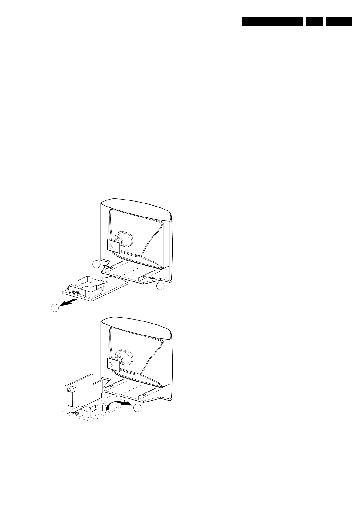
4.2 Service Position Main Panel
1. Disconnect the strain relief of the Mains cord.
2. Remove the main panel, by pushing the two centre clips
outward [1]. At the same time pull the panel away from the
CRT [2].
3. Disconnect the degaussing coil by removing the cable from
connector KP02.
4. Move the panel somewhat to the left and flip it 90 degrees
[3], with the components towards the CRT.
4.3 Rear Cover Mounting
Before you mount the rear cover:
1. Place the mains cord correctly in its guiding brackets
(strain relief).
2. Place all cables in their original position.
1
1
2
A
3
B
CL 36532010_023.eps
250203
Figure 4-1 Service Position
Page 8
EN 8 TE1.1E5.
Service Modes, Error Codes, and Fault Finding
5. Service Modes, Error Codes, and Fault Finding
Index of this chapter
1. Service Mode
2. ComPair
5.1 Service Mode
5.1.1 Introduction
The Service Mode offers features, which the service technician
can use to repair a set.
Any feature change, made via the Service Menu, will respond
at the same time (for example; if the Hotel Mode is enabled,
volume cannot be increased above max. volume displayed at
the Service Menu). But the response will be stored to NVM
while exiting from service menu.
All displayed text strings in the Service Mode are in English.
T T T T T L L L L L L X.X
E R R X X X X X
IF 38.9
3
Figure 5-2 Service Mode menu
CL 36532010_025.eps
250803
5.1.2 Purpose
• To create a pre-defined situation
• To change predefined options
• To enable the Hotel Mode, to change the Hotel Model
volume level
• To change configurations
• To align parameters in the Service Mode (e.g. colour
adjustment and geometry alignments)
NORMAL
OPERATION
RC button
or
Keyboard button
STANDBY OFF
RC button
"MENU"
"Exit"
Service Mode
RC button
"Standby"
Mains ON
RC button
"i+"
Mains OFF
Service Mode
(Display menu)
Make alignments (e.g. Colour adjustment and
geometry alignments), (de)select options,
Display information, Hotel Mode operations,
RC sequence
"0-6-2-5-9-6-i+"
Overide
software
protections
Options, etc.
CL 36532010_024.eps
250803
Explanation:
TTTTT - Life time counter
LLLLLL - Software Version name
X.X - Software cluster and version. Main changes are
displayed at the first digit and the second digit displays the
number of minor changes.
Function name - In this picture IF 38.9 displayed as an
example.
5.1.4 How to navigate
• Select the menu items with the CURSOR UP/DOWN
buttons. The selected item will be highlighted.
• Change the value of the menu items with the CURSOR
LEFT/RIGHT buttons. The selected item will be decreased
or increased or the previous/ next value (from a carrousel)
will be assigned. The new item value will be updated in the
related hardware function.
• Volume control and P+, P- are separated functions in the
service menus. These values can be altered while service
menu is open.
5.1.5 How to exit
• With the STANDBY command. The set switches to
Standby.
• With the Menu button or the i+ button. It causes to close all
of the menu items. The Service menu closes.
Switching the set 'off' and 'on' with the mains switch, brings the
set into normal operation again.
All changes in the Service Mode are stored immediately.
Figure 5-1 The Flow Chart Service menu
5.1.3 How to enter the Service Mode
Screen menu's must be 'off', when you enter the Service Mode.
Use a standard customer RC-transmitter sequence: 06, (then
within OSD time-out) 25, (then within OSD time-out) 96, (then
within OSD time-out) i+ button.
The following screen is visible when you enter the Service
Mode:
5.2 ComPair Mode
5.2.1 Introduction
ComPair (Computer Aided Repair) is a service tool for Philips
Consumer Electronics products. ComPair is a further
development on the European DST (Dealer Service Tool),
which allows faster and more accurate diagnostics. ComPair
has three big advantages:
• ComPair helps you to quickly get an understanding on how
to repair the chassis in a short time by guiding you
systematically through the repair procedures.
• ComPair allows very detailed diagnostics (on I
is therefore capable of accurately indicating problem areas.
You do not have to know anything about I
yourself because ComPair takes care of this.
• ComPair speeds up the repair time since it can
automatically communicate with the chassis (when the
microprocessor is working) and all repair information is
2
C level) and
2
C commands
Page 9

directly available. When ComPair is installed together with
the SearchMan electronic manual of the defective chassis,
schematics and PWBs are only a mouse click away.
5.2.2 Specifications
Service Modes, Error Codes, and Fault Finding
EN 9TE1.1E 5.
ComPair consists of a Windows based faultfinding program
and an interface box between PC and the (defective) product.
The ComPair interface box is connected to the PC via a serial
or RS232 cable.
The ComPair interface box and the TV communicate via a bidirectional service cable via the service connector.
The ComPair faultfinding program is able to determine the
problem of the defective TV set. ComPair can gather diagnostic
information in two ways:
• Automatic (by communication with the TV set): ComPair
can automatically read out the contents of the entire error
buffer. Diagnosis is done on I2C level. ComPair can send
and receive commands to the micro controller of the TV
set, and so can access the I2C bus of the TV set. In this
way, it is possible for ComPair to communicate (read and
write) to devices on the I2C busses of the TV set.
• Manually (by asking questions to you): Automatic
diagnosis is only possible if the micro controller of the TV
set is working correctly and only to a certain extend. When
this is not the case, ComPair will guide you through the
faultfinding tree by asking you questions (e.g. Does the
screen give a picture? Click on the correct answer: YES /
NO) and showing you examples (e.g. Measure test-point
F7 and click on the correct oscillogram you see on the
oscilloscope). You can answer by clicking on a link (e.g.
text or a waveform picture) that will bring you to the next
step in the faultfinding process.
By a combination of automatic diagnostics and an interactive
question / answer procedure, ComPair will enable you to find
most problems in a fast and effective way.
Beside fault finding, ComPair provides some additional
features like:
• Emulation of the (European) Dealer Service Tool (DST).
• If both ComPair and SearchMan (Electronic Service
Manual) are installed, all the schematics and the PWBs of
the set are available by clicking on the appropriate
hyperlink.
Example: Measure the DC-voltage on capacitor C2228
(Schematic/Panel). Click on the 'Panel' hyperlink to
automatically show the PWB with a highlighted capacitor
C2228. Click on the 'Schematic' hyperlink to automatically
show the position of the highlighted capacitor.
EXTERNAL 2
L
R
AUDIO EXTERNAL 1
SERVICE
CONNECTOR
PC VCR I2CPower
9V DC
CL96532156_029.eps
Figure 5-3 ComPair interface connection CL 96532156-029
5.2.4 How to Order
ComPair order codes:
• ComPair/SearchMan introduction package: 3122 785
90450.
• ComPair32 software (CD): 3122 785 60110.
• ComPair/I2C interconnection cable: 3122 785 90004
190600
5.2.3 How to Connect
1. First install the ComPair Browser software (see the Quick
Reference Card for installation instructions).
2. Connect the RS232 interface cable between a free serial
(COM) port of your PC and the PC connector (marked with
‘PC’) of the ComPair interface.
3. Connect the mains adapter to the supply connector
(marked with ‘POWER 9V DC’) of the ComPair interface.
4. Switch the ComPair interface ’OFF’.
5. Switch the television set ‘OFF’ with the mains switch.
6. Connect the ComPair interface cable between the
connector on the rear side of the ComPair interface
(marked with ‘I2C’) and the ComPair connector at the rear
side of the TV (situated just below the tuner input, see also
chapter 4).
7. Plug the mains adapter in a mains outlet, and switch the
interface ‘ON’. The green and red LEDs light up together.
The red LED extinguishes after approx. 1 second while the
green LED remains lit.
8. Start the ComPair program and read the ‘Introduction’
chapter.
Page 10

EN 10 TE1.1E5.
Personal Notes:
Service Modes, Error Codes, and Fault Finding
Page 11
Block Diagrams, Test Point Overview, and Waveforms
)
)
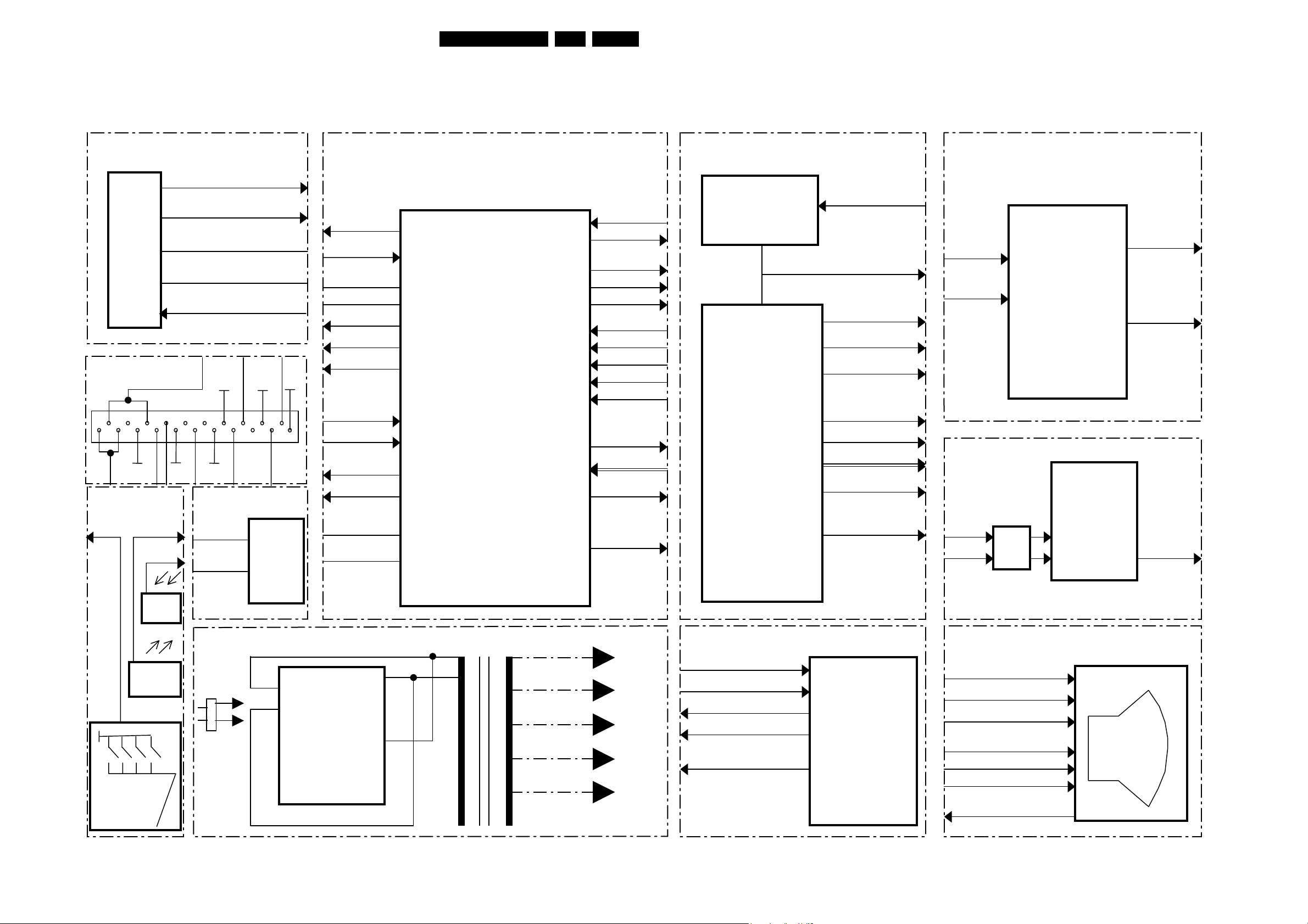
6. Block Diagrams, Test Point Overview, and Waveforms
Block Diagram
11TE1.1E 6.
A07 Tuner
TU01
11
10
5
4
1
A03 Scart
AUDIO IN
2 3 4
13
6 7 8
(A01 - 1)
(A01 - 64)
1
A11 IR+L ED
Keyboard
(A01 -7)
IF1 (A01-23 / A13)
IF2 (A01 – 24)
SDA (A01 – 3)
SCL (A01 – 2)
AGC (A01 – 27)
SWITCH
RGB
17
SWITCH
VI DEO
12
11
G
10
21
18
15
16
R
A09 EEProm
SDA1
(A01 - 63)
SCL1
(A01 - 62)
CVBS IN
5
14
CVBS
OUT
5
6
19
20
SCART1
KE01
IC02
24C16
A01 Microcontroller + VideoProcessor
A06 Horizontal
A12 Audio Amplifier
HORIZONTAL
1
RHOT (A11)
LED (A11)
B0 ( A02)
G0 (A12)
R0 (A12)
BLK IN (A05- 8
BCL IN (A05)
(A03)
G2/ YIN (A03)
R2 / VIN (A03)
AM OUT (A12 - 3)
CVBS/Y
STATUS
EHT0 (A06 - 8)
HOUT ( A06)
CVBS INT (A03)
MUTE (A12 - 5 )
KEYB (A11)
SCL (A07 - 4)
(A07 - 5
SDA
SW 1 (A13)
IDRV- (A05 - 2)
IDRV+ (A05 - 1)
9
IF IN1 (A07 - )
IF IN 2 (A07 - 10)
AGC
OUT (A07 - 1)
AV DEEM (A03 / A13 -8)
5
IV01
7
2
3
11
21
22
23
24
27
28
TDA9351
SDA1 (A09 - 5)
SCL1 (A09 - 6)
63
62
64
53
52
51
50
49
48
47
46
44
42
36
33
40
DRIVER +
FLYBACK
TRANSISTOR
WD02
1
FBT
8
5
9
6
7
4
(A01 - 33)
TO DEFLECTION YOKE
EHT (A02)
FOCUS (A02)
SCREEN (A02)
ABL (A01 - 36)
HEATER (A02)
16V (A05)
45V (A05)
8V (A01)
200V (A02)
IA50
(A01 - 44)
Vin
Vcont Out-
A01- 5
TDA7056A
3
5
6
8
A13 Secam L/L' Mono
IL01
TDA9830
IF1 (A07 - 11)
SW1 (A0 1 - 11)
IF
SWITCH
BLOCK
IF In
IF In
1
6
8
AF Out
(A01 - 28)
Out+
IR
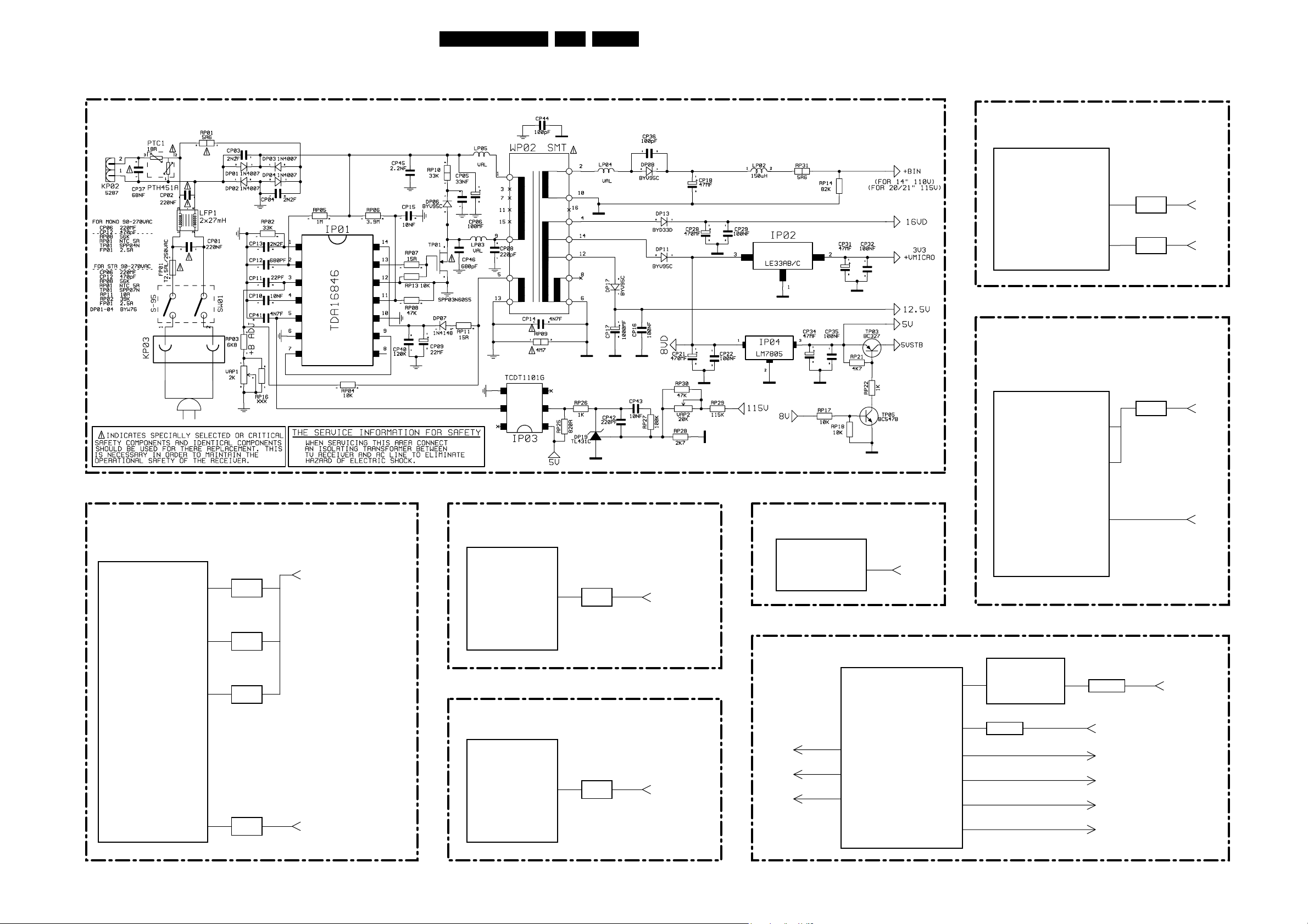
A04 Power Supply
WP0
110V
LED
2
3
AC IN
IP01
TDA16846
14
11
16V
3.3V
12.5V
5V
A05 Vertical
DRV+ (A01 - 22)
DRV- (A01 - 21)
V0(B) (TO VER. DEF. YOKE)
V0(A) (TO VER. DEF. YOKE)
V(GUARD) (A01 - 50)
1
2
4
7
8
ID50
TDA8356
A02 CRT Block
EHT (A06)
FOCUS (A06)
G2 (A06)
R0 (A01 -51)
G0 (A01 -52)
B0 (A01 - 53)
BLK IN
CL 36532010_013.eps
190203
Page 12

Block Diagrams, Test Point Overview, and Waveforms
12TE1.1E 6.
I2C Diagram
A1
TUNER
5
4
SDA
SCL
RT15
RT14
A2
SDA
SCL
RV24
3
2
Micro
Controller
+ VIDEO
PROC.
RV28
63
62
RV54
RV53
A4
SDA1
SCL1
RC47
6
EEPROM
5
RC30
SERVICE
SDA
SCL
SD
SCL1
KC03
CL 36532010_015.eps
Personal Notes:
190203
Page 13
Block Diagrams, Test Point Overview, and Waveforms
Supply Voltage Diagram
13TE1.1E 6.
A04 Power Supply
A05 Vertical
ID50
TDA 8356
A07 Tuner
TU01
TUNER
RD53
3
RD56
6
LT 07
6
16V
45V
A01 Microcontroller + VideoProcessor
IV01
LV06
TDA 9351
61
56
54
14
LV06
LV05
LV04
LV01
3.3V
8V
A12 Audio Amplifier
IA50
TDA 7056
RA51
2
A13 Secam L/L' Mono
IA50
TDA 983 0
RL25
12.5V
8V
A09 EEProm
IC02
24C16
9
A06 Horizontal
FBT
EHT
FOCUS
SCREEN
+Vmem
WD02
7
9
HORIZONTAL
1
2
4
9
6
7
DRIVE +
FLYBACK
TANSISTOR
RD31
RD05
110V
200V
16V
45V
8V
CL 36532010_014.eps
3.3V
16V
190203
Page 14
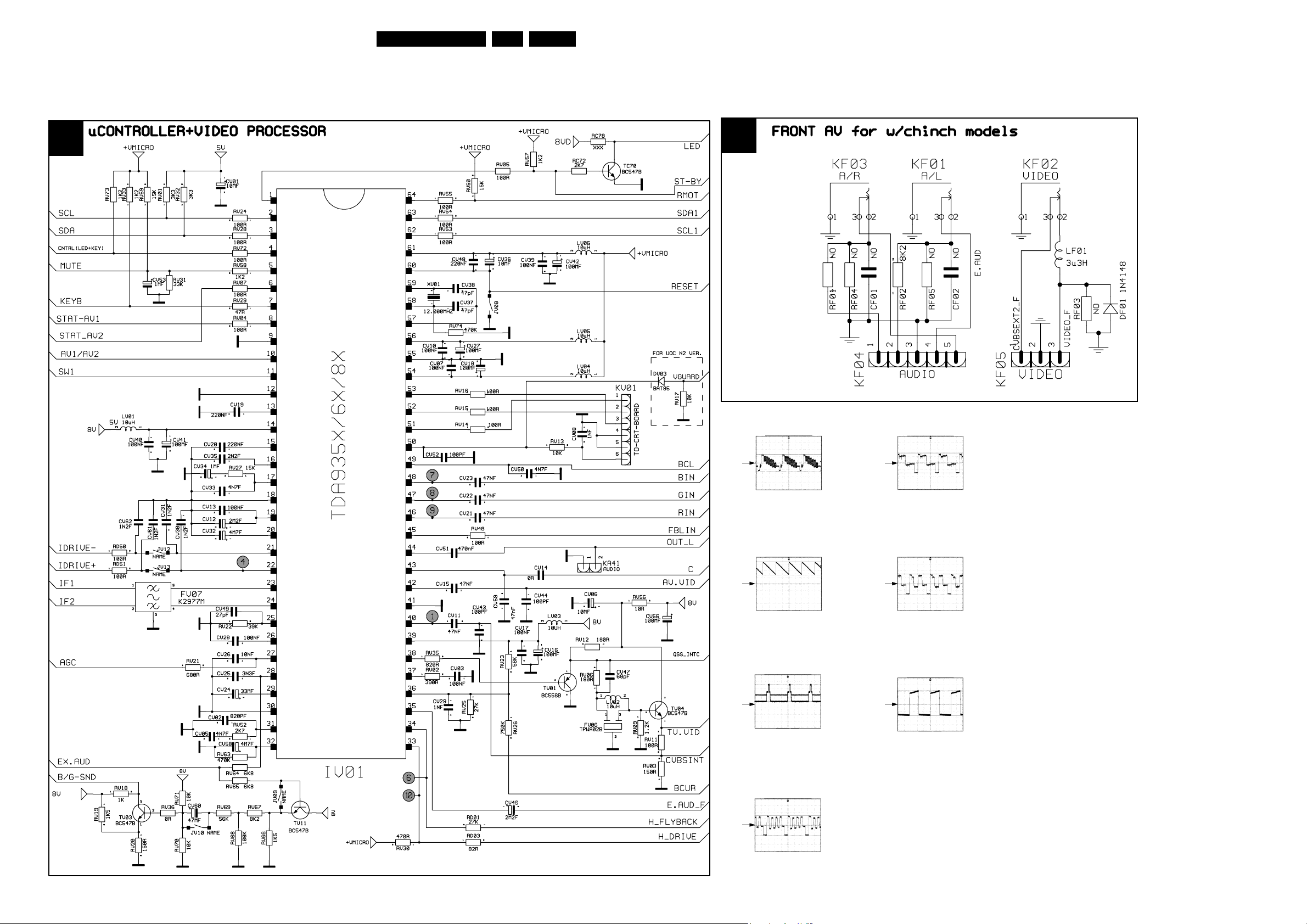
Circuit Diagrams and PWB Layouts
7. Circuit Diagrams and PWB Layouts
Main Panel: uController + Video Processor and Front AV
14TE1.1E 7.
A1
A2
TP01
TP08
500mV/div AC
20µs/div
TP04
1V/div AC
10ms/div
TP06
2V/div DC
20µs/div
TP07
500mV/div AC
20µs/div
TP09
500mV/div AC
20µs/div
TP10
500mV/div AC
20µs/div
500mV/div AC
20µs/div
CL 36532010_001.eps
190203
Page 15
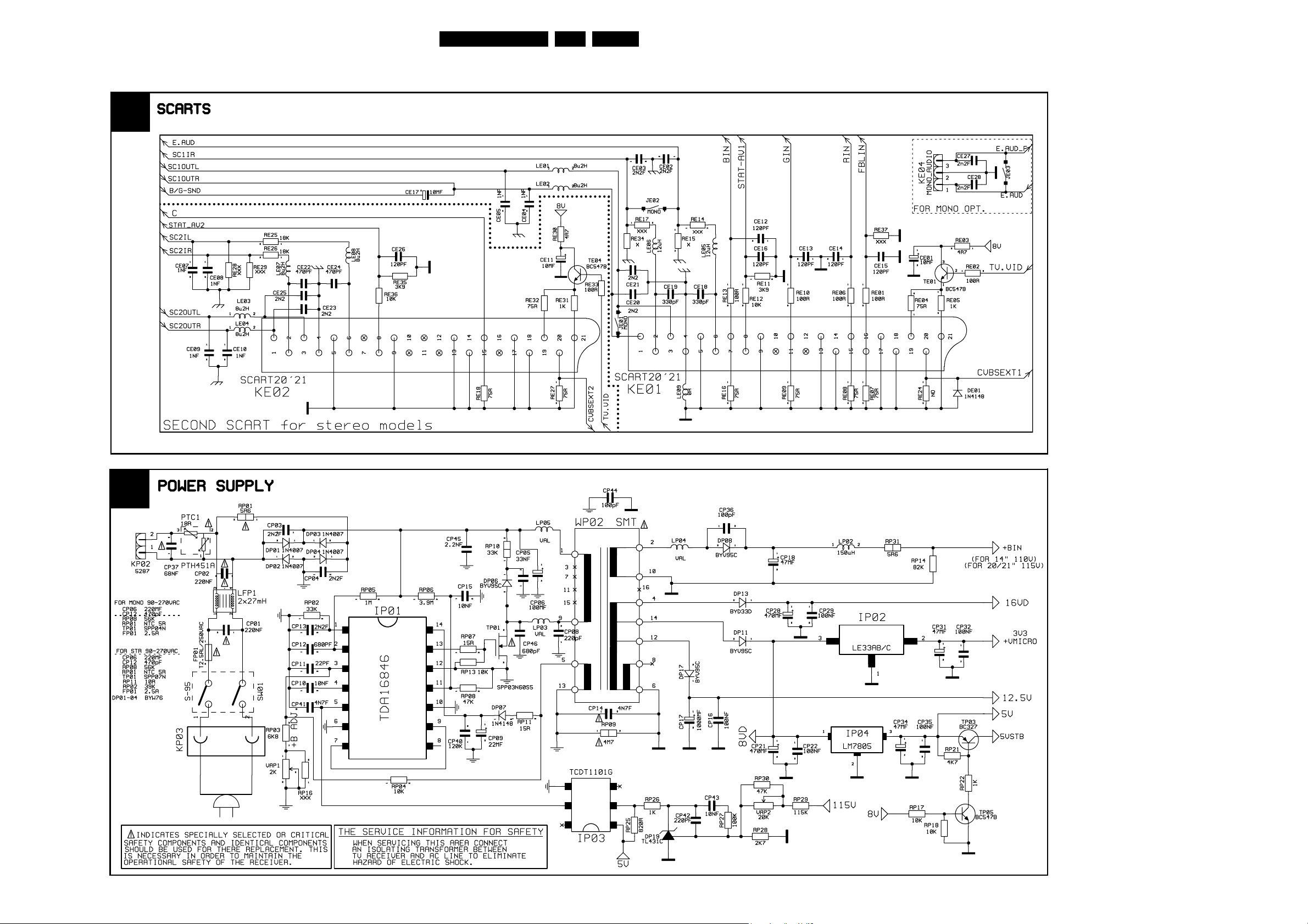
Circuit Diagrams and PWB Layouts
Main Panel: SCARTS and Power Supply
A3
15TE1.1E 7.
A4
CL 36532010_002.eps
190203
Page 16
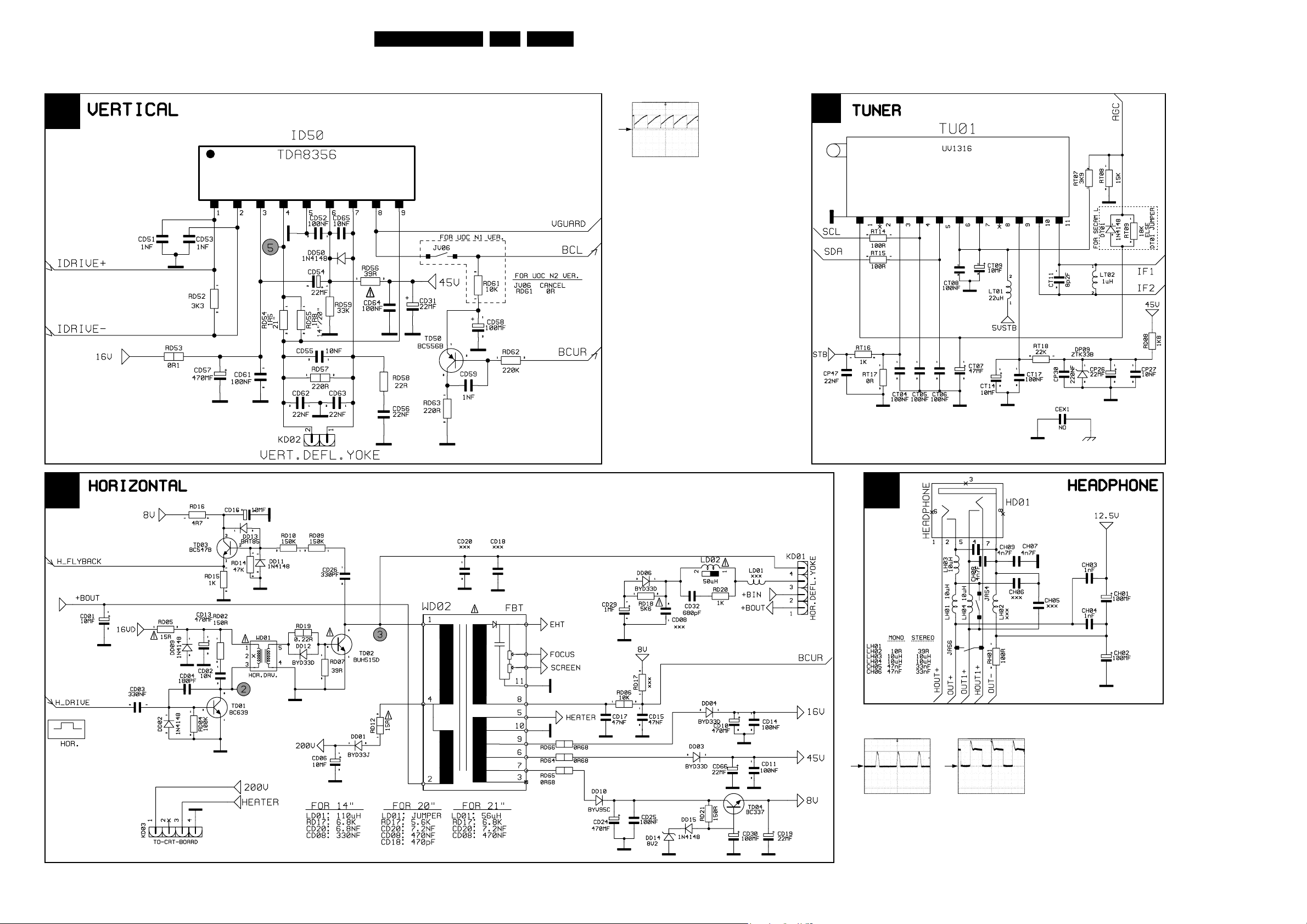
Circuit Diagrams and PWB Layouts
Main Panel: Vertical, Horizontal, Tuner and Headphone
A5
16TE1.1E 7.
TP05
A7
5V/div DC
10ms/div
A6
A8
TP02
5V/div DC
20µs/div
TP03
10V/div DC
20µs/div
CL 36532010_003.eps
190203
Page 17
Circuit Diagrams and PWB Layouts
17TE1.1E 7.
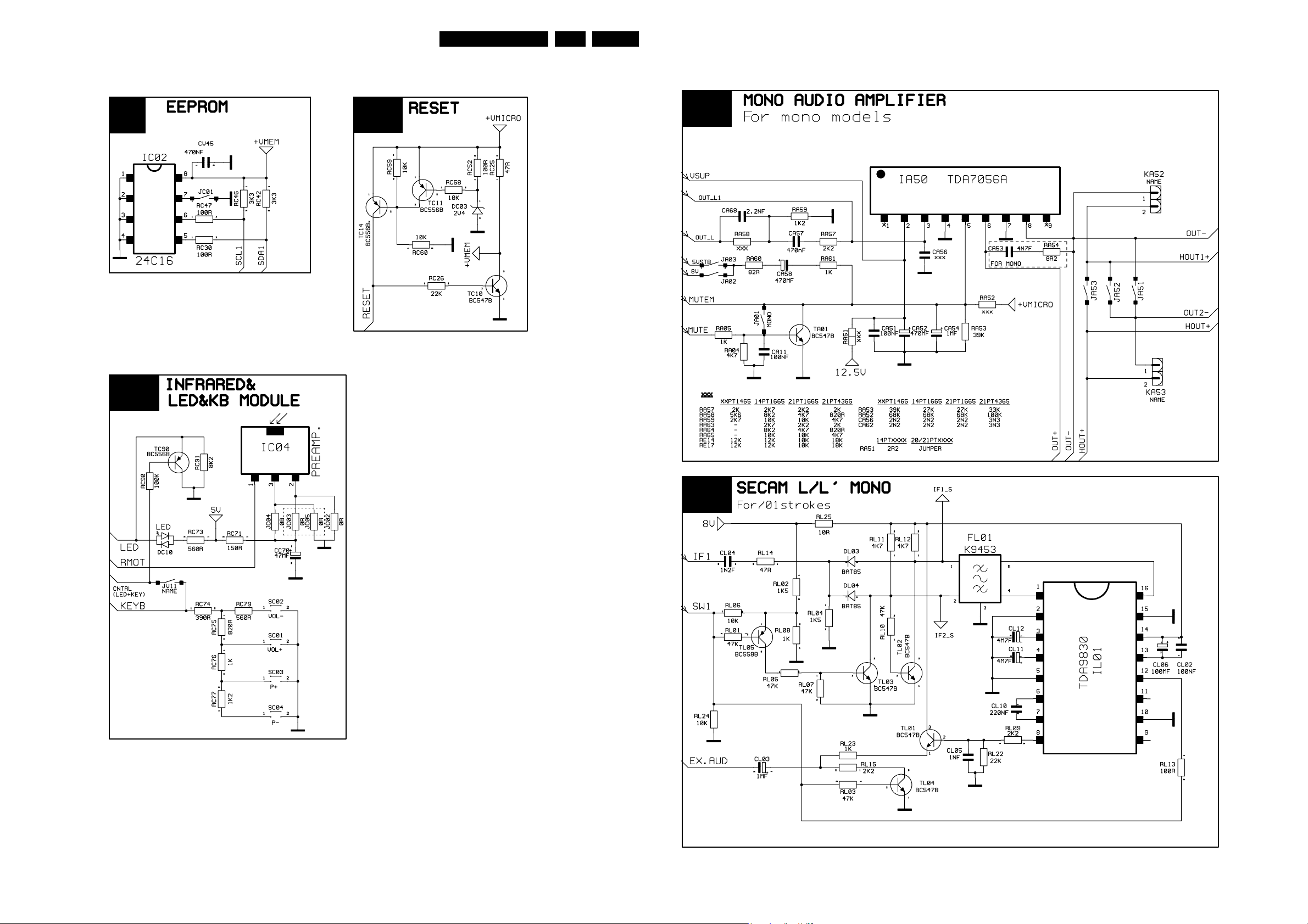
Main Panel: Eeprom, Reset and Infrared & LED & KB
A9
A10
Main Panel: Mono Audio Amplifier and SECAM L/L’ Mono
A12
A11
A13
CL 36532010_004.eps
250203
CL 36532010_022.eps
250203
Page 18
Circuit Diagrams and PWB Layouts
Layout Main Panel (Top Side)
18TE1.1E 7.
CL 36532010_008.eps
180203
Page 19

Circuit Diagrams and PWB Layouts
Layout Main Panel (Bottom Side)
19TE1.1E 7.
CL 36532010_009.eps
180203
Page 20

Circuit Diagrams and PWB Layouts
Main Panel: 2W Version (From DC1B Onwards) Micro controller + Video Processor and Front AV
20TE1.1E 7.
A1
MICRO CONTROLLER + VIDEO PROCESSOR
A2
FRONT AV FOR
W/CINCH MODELS
CL 36532010_026.eps
180903
Page 21

Circuit Diagrams and PWB Layouts
Main Panel: 2W Version (From DC1B Onwards) Scarts and Power Supply
SCARTS
A3
21TE1.1E 7.
A4
POWER SUPPLY
CL 36532010_027.eps
180903
Page 22

Circuit Diagrams and PWB Layouts
Main Panel: 2W Version (From DC1B Onwards) Vertical , Horizontal,Tuner, and Headphone
22TE1.1E 7.
A5
A6
VERTICAL
HORIZONTAL
A7
TUNER
A8
HEADPHONE
CL 36532010_032.eps
180903
Page 23

Circuit Diagrams and PWB Layouts
23TE1.1E 7.
Main Panel: 2W Version (From DC1B Onwards) EEPROM, Reset, and Infra Red
EEPROM
A9
A11
A10
INFRA RED + LED
+ KB SERVICE
RESET
Main Panel: 2W Version (From DC1B Onwards) Audio Amplifier,
SECAM L/L” Mono for Icon TV Strokes, and Stereo Connectors
AUDIO AMPLIFIER
A12
SECAM L/L' MONO FOR ICON TV/01 STROKES
A13
CL 36532010_031.eps
180903
A16
MSP STEREO
CONNECTORS
CL 36532010_028.eps
180903
Page 24

Circuit Diagrams and PWB Layouts
Layout Main Panel: 2W Version (From DC1B Onwards) (Top Side)
24TE1.1E 7.
CL 36532010_029.eps
120903
Page 25

Circuit Diagrams and PWB Layouts
Layout Main Panel: 2W Version (From DC1B Onwards) (Bottom Side)
25TE1.1E 7.
CL 36532010_030.eps
120903
Page 26

Circuit Diagrams and PWB Layouts
26TE1.1E 7.
CRT Board
B1
Layout CRT Board (Top Side)
CL 36532010_011.eps
180203
CL 36532010_005.eps
190203
Layout CRT Panel (Bottom Side)
CL 36532010_010.eps
190203
Page 27

8. Electrical Alignments
Electrical Alignments
EN 27TE1.1E 8.
Index of this chapter
1. Hardware Alignments
2. Software Alignments/Settings
8.1 Hardware Alignments
8.1.1 System Voltage Adjustment
• Switch the TV in AV mode by pressing the AV button on the
remote control unit (minimum beam current condition).
• Adjust the VAP1 potentiometer until you measure 110Vdc
for 14” or 115 Vdc for 20” on the cathode of diode DP08.
8.2 Software Alignments/Settings
Enter the Service Mode (see chapter 5). The Service Mode
menu will now appear on the screen.
The first screen that is displayed is of the IF adjustment. With
the CURSUR DOWN key the next menu item will be displayed.
The value can be changed with the LEFT/RIGHT CURSOR
keys.
8.2.1 Adjustments
IF: You can select the following IF frequencies: 38.9, 38.0, 58.8
and 45.8 MHz
Default value is 38.9 for PAL BG, DK and L and 33.4 for PAL L’.
IFL1: You can select the following IF frequencies: 33.4 and
33.9 MHz
Default value is 33.9
Connect a PLL pattern generator to the TV and select a
crosshatch pattern. Enter the service menu as described in
chapter 5 and perform the geometry adjustments HP, HB, HS,
VA, VS and VSH.
Press the MENU or OSD key to leave the service menu.
HP: Horizontal Parallelogram. Default value is 31.
HB: Horizontal Bow. Default value is 31.
HS: Horizontal Shift. Default value is 33.
VS: Vertical Slope. Default value is 29.
VA: Vertical Amplitude. Default value is 51.
SC: S-Correction. Default value is 15.
VSD: Vertical Scan Disable. Default value is off. With this bit
the G2 can be adjusted. When this item is selected information
about the G2 is displayed (INCR, OK, DECR). Turn the G2
potentiometer on the LOT until the screen displays “OK”.
“INCR” means the G2 must be increased and “DECR” means
the G2 must be decreased.
VSH: Vertical Shift. Default value is 41.
Connect a pattern generator to the TV and select a colour bar.
Set the contrast to 70%, brightness in the middle and the colour
saturation in the middle. Enter the service menu as described
in chapter 5 and perform the video adjustments BLR, BLG,
WPR, WPG, WPB, Ys, Yn, Yp and Yo.
Press the MENU or OSD key to leave the service menu.
BLR: Black Level Red. Default value is 32.
BLG: Black Level Green. Default value is 31.
WPR: White Point Red. Default value is 40.WPG: White
Point Green. Default value is 32.WPB: White Point Blue.
Default value is 32.Ys: Y-delay for SECAM. Default value is 5.
Yn: Y-delay for NTSC. Default value is 5.
Yp: Y-delay for PAL. Default value is 5.
Yo: Y-delay for external. Default value is 5.
AGC: Automatic gain control. Default value is 30.
CL: Cathode Drive level. Default value is 6.
Bits0 00: ACL, FCO, SVO, HP2, FSL, OSO:
These bits are control bits of the video processor. The default
value is 0.
It is advised to keep these bits on the default value.
Bits1 18: FFI, BTSC, FMWS, BKS, IFS:
These bits are control bits of the video processor.
The default values are:
FFI = 0
BTSC = 0
FMWS = 0
BKS = 1
IFS = 1
It is advised to keep these bits on the default value.
TXT-CL: Teletext Cathode Drive level. Default value is 5
8.2.2 Options
Options are used to control the presence/absence of certain
features and hardware.
An Option byte represents a number of different options. All
options are controlled via six option bytes.
How to change an Option byte
Use a LEFT/RIGHT CURSOR keys to change the option byte.
The byte values will change from 00 to FF.
Op1 87
PAL-BG 1
PAL-DK 1
PAL-I 1
PAL-M 0
PAL-N 0
NTSC-M 0
NTSC-443 0
SECAM-BG 1
CL 36532010_020.eps
200203
Figure 8-1 Option Code Screen
Option byte 1 (Op1)
PAL-BG
1: PAL BG available
0: PAL BG not available
Default setting = 1
PAL-DK
1: PAL DK available
0: PAL DK not available
Default setting = 1
PAL-I
1: PAL I available
0: PAL I not available
Default setting = 1
PAL-M
1: PAL M available
0: PAL M not available
Default setting = 0
PAL-N
1: PAL N available
0: PAL N not available
Default setting = 0
NTSC-M
1: NTSC M available
0: NTSC M not available
Default setting = 1
NTSC-443
1: NTSC 4.43 available
0: NTSC 4.43 not available
Default setting = 1
SECAM_BG
1: SECAM BG available
0: SECAM BG not available
Page 28

EN 28 TE1.1E8.
Electrical Alignments
Default setting = 1
Option byte 2 (Op2)
SECAM DK
1: SECAM DK available
0: SECAM DK not available
Default setting = 1
FRANCE
1: FRANCE available
0: FRANCE not
Default setting = 1
SYS-FR
1: System France available
0: System France not available
Default setting = 1
SYS-UK
1: System UK available
0: System UK not available
Default setting = 1
AV2
1: AV2 available
0: AV2 not available
Default setting = 0
AV-S
1: AV-S available
0: AV-S not available
Default setting = 0
AV3
1: AV3 available
0: AV3 not available
Default setting = 0
AV3S
1: AV3S available
0: AV3S not available
Default setting = 0
Option byte 3 (Op3)
JR
1: Stereo volume control via PWM-DACs enabled
0: Stereo volume control via PWM-DACs disabled
Default setting = 0
HP
1: reserved*
0: reserved*
Default setting = 0
Vbar
1: Volume bar OSD enabled
0: Volume bar OSD disabled
Default setting = 1
SubWoof
1: reserved*
0: reserved*
Default setting = 0
Presets
1: Predefined settings are available
0: Predefined settings are not available
Default setting = 1
Lock
1: reserved*
0: reserved*
Default setting = 1
Hotel
1: Hotel mode enabled
0: Hotel mode disabled
Default setting = 0
Option byte 4 (Op4)
16:9
1: 16:9 enabled
0: 16:9 disabled
Default setting = 0
110
1: 110 Deg. Picture tube
0: 90 Deg. Picture tube
Default setting = 0
Hpol
1: Polarity of the Horizontal sync for OSD is negative
0: Polarity of the Horizontal sync for OSD is positive
Default setting = 0
Vpol
1: Polarity of the Vertical sync for OSD is negative
0: Polarity of the Vertical sync for OSD is positive
Default setting = 0
Field
When set, the vertical sync for OSD is in the second half line at
the start of an even field. When not set in the first half line at the
start of an even field.
1: enabled
0: disabled
Default setting = 1
FEOut
1: CVBS signal always present on AV1
0: CVBS signal not always present on AV1
Default setting = 1
Swon
1: Last status enabled
0: Last status disabled
Default setting = 1
VGCheck
When service mode is activated vertical guard is switched off.
1: VG Check enabled
0: VG Check disabled
Default setting = 1
Option byte 5 (Op5)
Clock
1: Clock menu enabled
0: Clock menu disabled
Default setting = 1
AM/PM
1: AM/PM enabled
0: AM/PM disabled
Default setting = 0
AVL
1: Automatic Volume Level enabled
0: Automatic Volume Level disabled
Default setting = 1
1norma
1: reserved*
0: reserved*
Default setting = 0
FLOF-TXT
1: FLOF TXT on
0: FOLF TXT off
Default setting = 1
TR
1: Sound is not muted in weak signals
0: Sound is muted in weak signals
Default setting = 0
P-AND-P
1: Plug and Play enabled
0: Plug and Play disabled
Default setting = 1
Option byte 6 (Op6)
UOC-J
1: reserved*
0: reserved*
Default setting = 0
IgnrSUP
1: Ignore the status of SUP at power on
0: Not ignore the status of SUP at power on
Default setting = 0
Ignr NDF
1: Ignore the status of NDF at power on
Page 29

0: Not ignore the status of NDF at power on
Default setting = 1
TXT on
1: Teletext available
0: Teletext not available
Default setting = 0
SYS-DK
1: System DK available
0: System DK not available
Default setting = 1
WSS
1: Wide Screen Signalling bit enabled
0: Wide Screen Signalling bit disabled
Default setting = 0
Note:
• Reserved bits (*) must be set to 0.
• The 7th bit of Option byte 03 enables the "no video ident"
timer.
8.2.3 Tune IF
TSL:
Start frequency of the low-band in MHz.
TEL:
End frequency of the low-band in MHz.
TSM:
Start frequency of the mid-band in MHz.
TEM:
Start frequency of the mid-band in MHz.
TSH:
Start frequency of the high-band in MHz.
TEH:
Start frequency of the high-band in MHz.
TBL:
Hex value needed for switching to the low-band.
TBM:
Hex value needed for switching to the mid-band.
TBH:
Hex value needed for switching to the high-band.
Electrical Alignments
EN 29TE1.1E 8.
Tuner Type Philips Orega Temic Samsung Alps
TSL 45454545 45
TEL 160 118 150 150 180
TSM 160 118 150 150 180
TEM 440 400 440 425 465
TSH 440 400 440 425 465
TMH 863 865 865 865 900
TBL A1311 1
TBM 92622 2
TBH 34854 8 0C
8.2.4 Hotel Mode
Installation and Child Lock Menus are omitted in Hotel Mode.
You cannot search any channel when the Hotel Mode is
activated.
8.2.5 Volume
In Hotel Mode the volume level cannot be increased higher
then the level adjusted in the Service Mode.
Page 30

EN 30 TE1.1E9.
Circuit Descriptions, List of Abbreviations, and IC Data Sheets
9. Circuit Descriptions, List of Abbreviations, and IC Data Sheets
9.1 Circuit Descriptions
Not applicable.
9.2 Abbreviation List
Doc Depends on Chassis
CH- Channel minus
CH+ Channel plus
Vol+ Volume +
Vol- Volume IF1 Intermediate Frequency 1
IF2 Intermediate Frequency 2
SCL I2C Clock
AGC Auto Gain Control
SDA I2C Data
FBEXT Fast Blanking External
RRed
G Green
BBlue
CVBSEXT1 External Composite Video Signal
SC_OUT Scart out
SC_IN Scart in
CVBS Composite Video Signal
KEYB Front panel keyboard
5VD 5 V digital
5VA 5 V analog
ST_BY Standby
HOUT Horizontal Output pulse
110VOUT 110 V Horizontal power supply
FBT Flayback Transformer
V_OSD Vertical OSD
V_AMP Vertical Amplitude DAC output
24V_VERT 24 V Vertical power supply
VERT Vertical Output pulse
AV1/AV2 AV1 / AV2 information
B_OSD OSD Blue input
G_OSD OSD Green input
R_OSD OSD Red input
FB_OSD OSD Fast blanking Input
CVBSOUT Second Video Switch Output
CVBSEXT External CVBS input
GNDA Analog Ground
AUDOUT Main Audio Output
VOL Volume
IR Infrared led
RMOT Remote Control
L/L’ Secam L/L’ sound standard
TXTSW Teletext switch
BCL Beam Current Limiter
FLM. Flaman
LOUT Left out
VGND Video ground
ON/STBY On/Standby
MDO Mode control data output
PRST Preset
VGUARD Vertical guard voltage
IDRIVE+ Vertical drive +
IDRIVE- Vertical drive VMICRO Power supply for micro controller
SW1 Switch 1
EX.AUD External audio
E.AUD ExternalAudio
SC1IA Scartin Audio
SC1OUTL Scartout Left
SC1OUTA Scartout Audio
B/G-SND BG Sound
TV.VID Video signal for TV
BIN Blue in
STAT-AV AV Status
GIN Green in
RIN Red in
FBLIN Fast blanking in
5VSTB Stand-by voltage
C Chromo
AV.VID Video signal for AV
BCUR Beam Current
E.AUD_F External Audio
H_FLYBACK Horizontal Flayback
H_DRIVE Horizontal Drive
VMEM Voltage supplied for Eepro
Page 31

Circuit Descriptions, List of Abbreviations, and IC Data Sheets
9.3 IC Data Sheets
In this paragraph, the internal block diagrams and pinning are
given of ICs that are drawn as a “black box” in the electrical
diagrams (with the exception of “memory” and “logic” ICs).
9.3.1 TCDT110(G) Series
EN 31TE1.1E 9.
Page 32

EN 32 TE1.1E9.
Circuit Descriptions, List of Abbreviations, and IC Data Sheets
Page 33

Circuit Descriptions, List of Abbreviations, and IC Data Sheets
EN 33TE1.1E 9.
Page 34

EN 34 TE1.1E9.
Circuit Descriptions, List of Abbreviations, and IC Data Sheets
Page 35

Circuit Descriptions, List of Abbreviations, and IC Data Sheets
EN 35TE1.1E 9.
Page 36

EN 36 TE1.1E9.
Circuit Descriptions, List of Abbreviations, and IC Data Sheets
Page 37

Circuit Descriptions, List of Abbreviations, and IC Data Sheets
EN 37TE1.1E 9.
Page 38

EN 38 TE1.1E9.
Circuit Descriptions, List of Abbreviations, and IC Data Sheets
Page 39

Circuit Descriptions, List of Abbreviations, and IC Data Sheets
EN 39TE1.1E 9.
Page 40

EN 40 TE1.1E9.
Circuit Descriptions, List of Abbreviations, and IC Data Sheets
Page 41

Circuit Descriptions, List of Abbreviations, and IC Data Sheets
EN 41TE1.1E 9.
Page 42

EN 42 TE1.1E9.
Circuit Descriptions, List of Abbreviations, and IC Data Sheets
Page 43

Circuit Descriptions, List of Abbreviations, and IC Data Sheets
EN 43TE1.1E 9.
Page 44

EN 44 TE1.1E9.
Circuit Descriptions, List of Abbreviations, and IC Data Sheets
Page 45

Circuit Descriptions, List of Abbreviations, and IC Data Sheets
EN 45TE1.1E 9.
Page 46

EN 46 TE1.1E9.
Circuit Descriptions, List of Abbreviations, and IC Data Sheets
Page 47

Circuit Descriptions, List of Abbreviations, and IC Data Sheets
EN 47TE1.1E 9.
Page 48

EN 48 TE1.1E9.
Circuit Descriptions, List of Abbreviations, and IC Data Sheets
Page 49

Circuit Descriptions, List of Abbreviations, and IC Data Sheets
EN 49TE1.1E 9.
Page 50

EN 50 TE1.1E9.
Circuit Descriptions, List of Abbreviations, and IC Data Sheets
Page 51

Circuit Descriptions, List of Abbreviations, and IC Data Sheets
EN 51TE1.1E 9.
Page 52

EN 52 TE1.1E10.
10. Spare Parts List
Spare Parts List
Monoboard + CRT panel [A] [B]
Various
A--E 0020 205 11220 Cable black 18cm
C--G 0020 205 11220 Cable black 18cm
FL01 0377 300 07771 Filter saw K9453M
FP01 0673 100 01831 Fuse T2.5A 250V
FP01 0751 102 11040 Fuse holder
FV06 0377 200 07821 Filter trap 6.0MHz
FV06 4822 242 10254 TPWA02B-TF21
FV07 0377 300 07821 Filter saw J1981M
FV07 0377 300 07991 Filter saw K2977M B/GD/
KA41 0750 302 11011 2P vert.
KA42 0020 205 11130 Cable 2P Shielded 15cm
KA42 0020 920 00250 Cable 2P 25cm
KA42 0750 302 11011 2P vert.
KC03 0751 007 11031 7P flat
KD01 0751 002 01010 4P hor. male
KD01 0751 002 01110 4P hor. male 5x5x7.5
KD02 0750 302 11001 2P vert. 5mm
KD03 0020 920 00450 Cable 4P(3P) white 45cm
KD03 0020 920 00510 Cable 4P(3P) 45cm
KE01 0750 402 10051 Socket scart
KE04 0020 411 00460 Cable 3P 35cm
KE06 0020 411 00460 Cable 3P 35cm
KEMC 0020 205 11160 Cable black 30cm
KF01 0050 150 24140 Protective cinch
KF01 0750 164 20381 Cinch socket Y/ W
KP02 0751 002 11781 2P 7.5mm
KP03 0750 302 61010 2P vert. 10mm
KV01 0025 215 17140 Cable 6P white 50cm
KV01 0025 215 17160 Cable 6P 38cm
SC01 0811 011 14031 Tact switch hor.
SC02 0811 011 14031 Tact switch hor.
SC03 0811 011 14031 Tact switch hor.
SC04 0811 011 14031 Tact switch hor.
SW01 0810 000 00141 Mains switch
SY04 0750 208 00031 CRT socket Narrow neck
TU01 6168 000 20001 Tuner CTT5020E/
XV01 0490 300 00091 Crystal 12.000 MHz
g
C004 0420 339 11011 3.3µF 250V
C004 0424 685 14791 6.8µF 250V
CA11 0400 670 41081 100nF 20% 50V 0805
CA51 0400 670 41081 100nF 20% 50V 0805
CA52 0424 492 54771 470µF 20% 25V
CA53 4822 126 13193 4.7nF 10% 63V
CA54 0424 165 01051 1µF 20% 50V
CA56 4822 126 14238 2.2nF 50V 0603
CA57 0400 440 81861 470nF 10% 16V 0603
CA58 0424 465 01061 10µF 20% 50V
CA68 4822 126 14238 2.2nF 50V 0603
CC70 0424 142 54761 47µF 20% 25V
CD01 0424 408 61061 10µF 20% 250V
CD02 6200 040 71031 10nF 10% 50V
CD03 5322 121 42661 330nF 5% 63V
CD06 0424 408 61061 10µF 20% 250V
CD08 6200 130 54741 470nF 5% 250V
CD08 6210 030 03351 330nF 5% 250V
CD10 0424 492 54771 470µF 20% 25V
CD11 6200 130 81041 100nF 5% 63V
CD13 0424 492 54771 470µF 20% 25V
CD14 0400 670 41081 100nF 20% 50V 0805
CD15 6210 040 04731 47nF 100V
CD16 0424 465 01061 10µF 20% 50V
CD17 6210 040 04731 47nF 100V
CD18 0400 401 74711 470pF 10% 2kV
CD19 0424 165 02261 22µF 20% 50V
CD20 6180 081 27211 7.2nF1.6kV
CD20 6193 237 76821 6.8nF 2.5% 1.6kV
CD24 0424 492 54771 470µF 20% 25V
CD25 0400 670 41081 100nF 20% 50V 0805
CD26 0400 402 53311 330pF 250V
CD28 0424 166 32261 22µF 63V
CD29 0424 148 61051 1µF 20% 250V
CD30 0421 401 61071 100µF 20% 16V
CD31 0424 166 32261 22µF 63V
CD32 0400 401 56811 680pF 10% 1kV
CD51 5322 126 11578 1nF 10% 50V 0603
CD52 6200 130 81041 100nF 5% 63V
CD53 5322 126 11578 1nF 10% 50V 0603
CD54 0424 166 32261 22µF 63V
5X20MM
K
CTF5510
CD55 6200 040 01051 10nF 50V
CD56 6180 130 12231 22nF 50V
CD57 0424 492 54771 470µF 20% 25V
CD58 0421 401 61071 100µF 20% 16V
CD58 0424 462 55661 56µF 25V
CD59 4822 126 13883 220pF 5% 50V
CD61 0400 670 41081 100nF 20% 50V 0805
CD64 6200 130 81041 100nF 5% 63V
CD65 5322 126 11583 10nF 10% 50V 0603
CD66 0424 166 32261 22µF 63V
CE01 0424 465 01061 10µF 20% 50V
CE02 4822 126 14238 2.2nF 50V 0603
CE03 4822 126 14238 2.2nF 50V 0603
CE04 0400 402 53361 330pF 10% 50V 0603
CE15 5322 122 33861 120pF10% 50V
CE16 5322 122 33861 120pF10% 50V
CE17 0424 465 01061 10µF 20% 50V
CE18 0400 402 53361 330pF 10% 50V 0603
CE19 0400 402 53361 330pF 10% 50V 0603
CE20 4822 126 14238 2.2nF 50V 0603
CE21 4822 126 14238 2.2nF 50V 0603
CE27 4822 126 14238 2.2nF 50V 0603
CE28 4822 126 14238 2.2nF 50V 0603
CH01 0421 401 61071 100µF 20% 16V
CH02 0421 401 61071 100µF 20% 16V
CH05 0400 700 44731 47nF 50V
CH06 0400 700 44731 47nF 50V
CH07 0400 400 44721 4.7nF 10% 50V
CL02 0400 670 41081 100nF 20% 50V 0805
CL03 0424 485 04761 47µF 20% 50V
CL04 2020 552 93683 1.2nF 10% 50V 0603
CL05 0400 402 53361 330pF 10% 50V 0603
CL06 0421 401 61071 100µF 20% 16V
CL10 0407 430 22261 220NF 20-80% 50V 0603
CL11 0421 945 04751 4.7µF 20% 50V
CL12 0421 945 04751 4.7µF 20% 50V
CL13 0400 130 71041 100nF 100V
CL14 5322 126 11583 10nF 10% 50V 0603
CP01 6200 040 62241 220nF 20% 275V
CP02 6200 040 62241 220nF 20% 275V
CP03 0400 401 52211 2.2nF 10% 1kV
CP04 0400 401 52211 2.2nF 10% 1kV
CP05 6200 041 33331 33nF 5% 630V
CP06 0427 199 01071 100µF 20 % 400V
CP08 0400 401 56811 680pF 10% 1kV
CP08 0400 401 72211 220pF 10% 2kV
CP09 0424 165 02261 22µF 20% 50V
CP10 5322 126 11583 10nF 10% 50V 0603
CP11 0400 310 42261 22pF 5% 50V 0603
CP12 0400 500 56861 680pF 5% 50V 0603
CP13 4822 126 14238 2.2nF 50V 0603
CP14 0400 402 02221 2.2nF 20% 400V
CP14 0402 587 64721 4.7nF 20% 400V
CP15 5322 126 11583 10nF 10% 50V 0603
CP16 0400 670 41081 100nF 20% 50V 0805
CP17 0424 402 51081 1000µF 20% 25V
CP18 0424 198 34761 47µF 20% 160V
CP21 0424 492 54771 470µF 20% 25V
CP22 0400 670 41081 100nF 20% 50V 0805
CP26 0424 165 02261 22µF 20% 50V
CP27 5322 126 11583 10nF 10% 50V 0603
CP28 0424 492 54771 470µF 20% 25V
CP29 0400 670 41081 100nF 20% 50V 0805
CP30 6200 040 72241 220nF 10% 63V
CP31 0424 142 54761 47µF 20% 25V
CP32 0400 670 41081 100nF 20% 50V 0805
CP34 0424 142 54761 47µF 20% 25V
CP35 0400 670 41081 100nF 20% 50V 0805
CP36 0400 501 51011 100pF 1kV
CP37 6200 050 76831 68nF 20% 275V
CP40 4822 051 30124 120k 5% 0.062W
CP44 0400 670 41371 1nF 20% 400V
CP45 0400 401 72221 2.2nF 2kV
CP46 0400 401 56811 680pF 10% 1kV
CP46 0400 401 72211 220pF 10% 2kV
CP47 0400 400 42261 22nF 20% 50V 0603
CT05 4822 126 11785 47pF 5% 50V 0603
CT06 4822 126 11785 47pF 5% 50V 0603
CT07 0424 142 54761 47µF 20% 25V
CT08 0400 670 41081 100nF 20% 50V 0805
CT09 0424 465 01061 10µF 20% 50V
CT14 0424 465 01061 10µF 20% 50V
CT17 0400 670 41081 100nF 20% 50V 0805
CV01 0424 465 01061 10µF 20% 50V
CV02 0407 320 82261 820pF 50V 0603
CV03 0400 670 41081 100nF 20% 50V 0805
CV05 4822 126 13193 4.7nF 10% 63V
CV06 0424 465 01061 10µF 20% 50V
CV07 0400 670 41081 100nF 20% 50V 0805
CV08 5322 126 11578 1nF 10% 50V 0603
CV10 0400 670 41081 100nF 20% 50V 0805
CV11 6210 040 04731 47nF 100V
CV12 0424 465 02251 2.2µF 20% 50V
CV13 0400 670 41081 100nF 20% 50V 0805
CV15 6210 030 04731 47nF 5% 50V
CV16 0421 401 61071 100µF 20% 16V
CV17 0400 670 41081 100nF 20% 50V 0805
CV18 0421 401 61071 100µF 20% 16V
CV19 6200 040 72241 220nF 10% 63V
CV20 6200 040 72241 220nF 10% 63V
CV21 0400 420 44861 47nF 10% 50V 0603
CV22 0400 420 44861 47nF 10% 50V 0603
CV23 0400 420 44861 47nF 10% 50V 0603
CV24 0424 171 63361 33µF 16V
CV24 0424 465 01061 10µF 20% 50V
CV25 5322 126 11579 3.3nF 10% 63V
CV26 5322 126 11583 10nF 10% 50V 0603
CV27 0421 401 61071 100µF 20% 16V
CV28 6200 130 81041 100nF 5% 63V
CV29 5322 126 11583 10nF 10% 50V 0603
CV30 2020 552 93683 1.2nF 10% 50V 0603
CV31 2020 552 93683 1.2nF 10% 50V 0603
CV32 0424 465 02251 2.2µF 20% 50V
CV33 4822 126 13193 4.7nF 10% 63V
CV34 0424 165 01051 1µF 20% 50V
CV35 4822 126 14238 2.2nF 50V 0603
CV36 0424 465 01061 10µF 20% 50V
CV37 0400 430 45661 56pF 5% 50V 0603
CV38 0400 430 45661 56pF 5% 50V 0603
CV39 0400 670 41081 100nF 20% 50V 0805
CV40 0400 670 41081 100nF 20% 50V 0805
CV41 0421 401 61071 100µF 20% 16V
CV42 0421 401 61071 100µF 20% 16V
CV43 0407 320 41081 100pF 5% 50V 0805
CV44 0407 320 41081 100pF 5% 50V 0805
CV45 0400 440 81861 470nF 10% 16V 0603
CV46 0424 465 02251 2.2µF 20% 50V
CV47 0407 320 41081 100pF 5% 50V 0805
CV48 0407 430 22261 220nF 20-80% 50V 0603
CV49 4822 126 11669 27pF
CV50 4822 126 13193 4.7nF 10% 63V
CV51 6200 040 04741 470nF 10% 50V
CV53 0424 165 01051 1µF 20% 50V
CV56 0421 401 61071 100µF 20% 16V
CV58 0424 165 01051 1µF 20% 50V
CV59 0400 420 44861 47nF 10% 50V 0603
CV61 4822 126 14241 330pF 50V 0603
CV62 4822 126 14241 330pF 50V 0603
CY01 0400 401 71021 1nF 10% 2kV
CY03 6210 041 33331 33nF 400V
CY04 0400 402 53361 330pF 10% 50V 0603
CY05 0400 402 53361 330pF 10% 50V 0603
CY06 0400 402 53361 330pF 10% 50V 0603
CY07 0424 468 62251 2.2µF 20% 250V
J137 0400 670 41081 100nF 20% 50V 0805
f
J125 4822 051 30008 Jumper 0603
J126 4822 051 30008 Jumper 0603
J129 4822 051 30008 Jumper 0603
J134 4822 051 30008 Jumper 0603
J135 4822 051 30008 Jumper 0603
J136 4822 051 30008 Jumper 0603
J143 4822 051 30008 Jumper 0603
J148 4822 051 30008 Jumper 0603
J151 4822 051 30008 Jumper 0603
J160 4822 051 30008 Jumper 0603
J161 4822 051 30008 Jumper 0603
J165 4822 051 30008 Jumper 0603
JA03 4822 051 30008 Jumper 0603
JA55 4822 051 30008 Jumper 0603
JC01 4822 051 30008 Jumper 0603
JC03 4822 051 30008 Jumper 0603
JC05 4822 051 30008 Jumper 0603
JE01 4822 051 30008 Jumper 0603
JE02 4822 051 30008 Jumper 0603
JV01 4822 051 30008 Jumper 0603
JV06 4822 051 30008 Jumper 0603
JV10 4822 051 30008 Jumper 0603
LH02 0300 506 22011 22Ω 5% 1/2W
LY04 0300 596 47811 0.47Ω 1W
PTC1 0347 103 03631 PTC 18Ω 30%
R001 0301 056 10911 1Ω 5% 1 W fus able
R001 0301 056 47811 0.47Ω 5% 1W
RA04 4822 051 30472 4k7 5% 0.062W
RA05 4822 051 30102 1k 5% 0.062W
RA51 0301 086 22921 2.2Ω 1W
Page 53

Spare Parts List
EN 53TE1.1E 10.
RA52 0300 206 68311 68K 5% 1/4W
RA53 4822 051 30393 39k 5% 0.062W
RA54 2322 702 81828 8.2Ω 5% 0.1W 0603
RA57 0300 106 83061 2K 5% 1/10W 0603
RA57 4822 051 30222 2k2 5% 0.062W
RA58 0300 116 56261 5.1K 1/10W 0603
RA58 4822 051 30562 5k6 5% 0.063W 0603
RA59 4822 051 30152 1k5 5% 0.062W
RA59 4822 051 30332 3k3 5% 0.062W
RA60 0300 206 82011 82Ω 1/4W
RA61 4822 051 30102 1k 5% 0.062W
RC25 4822 051 30479 47Ω 5% 0.062W
RC26 4822 051 30223 22k 5% 0.062W
RC30 4822 051 30101 100Ω 5% 0.062W
RC42 4822 051 30332 3k3 5% 0.062W
RC46 4822 051 30332 3k3 5% 0.062W
RC47 4822 051 30101 100Ω 5% 0.062W
RC52 4822 051 30101 100Ω 5% 0.062W
RC58 4822 051 30103 10k 5% 0.062W
RC59 4822 051 30103 10k 5% 0.062W
RC60 4822 051 30103 10k 5% 0.062W
RC71 0300 106 15161 150Ω 5% 1/10W 0603
RC72 5322 117 13052 2k7 1% 0.063W 0603
RC73 4822 051 30561 560Ω 5% 0.062W
RC74 4822 051 30391 390Ω 5% 0.062W
RC75 0300 106 82161 820Ω 5% 1/10W 0603
RC76 4822 051 30102 1k 5% 0.062W
RC77 0300 106 12261 1.2K 5% 1/10W 0603
RC79 4822 051 30561 560Ω 5% 0.062W
RC90 4822 117 13632 100k 1% 0603 0.62W
RC91 4822 117 12902 8k2 1% 0.063W 0603
RD01 4822 051 30273 27k 5% 0.062W
RD02 0300 206 15131 150Ω 5% 1/4W
RD03 5322 117 13068 82Ω 1% 0.063W 0603
RD04 4822 117 13632 100k 1% 0603 0.62W
RD05 0300 256 15001 15Ω 1/4W fusable
RD06 0300 506 10311 10K 1/2W
RD07 0300 506 39311 39Ω 1/4W
RD08 0300 206 18231 1.8K 1/4W
RD09 0300 206 15431 150K 5% 1/4W
RD10 0300 206 15431 150K 5% 1/4W
RD14 4822 117 12925 47k 1% 0.063W 0603
RD15 4822 051 30102 1k 5% 0.062W
RD16 0300 206 47911 4.7Ω 1/4W
RD17 0300 206 56231 5.6K 1/4W
RD17 0300 206 68211 6.8K 1/4W
RD18 0300 106 56221 5.6K 5% 1W fusable
RD19 0301 086 15511 0.22Ω 5% 1W
RD20 0300 206 10231 1K 5% 1/4W
RD21 0300 106 15161 150Ω 5% 1/10W 0603
RD50 0300 206 10131 100Ω 5% 1/4W
RD51 0300 206 10131 100Ω 5% 1/4W
RD52 4822 051 30332 3k3 5% 0.062W
RD53 0300 557 22811 0.22Ω 5% 1/2W fusable
RD54 0301 086 18911 1.8Ω 1W
RD56 0300 256 82011 82Ω 1/4W fuasable
RD57 0300 596 22211 220Ω 1W
RD58 0300 206 22011 22Ω 1/4W
RD59 4822 051 30333 33k 5% 0.062W
RD61 4822 051 30008 Jumper 0603
RD61 4822 051 30103 10k 5% 0.062W
RD62 5322 117 13039 220K 1% 0.063W 0603
RD63 4822 051 30221 220Ω 5% 0.062W
RD64 0300 556 68811 0.68Ω 1 /2W fu sabl e
RD65 0300 556 68811 0.68Ω 1 /2W fu sabl e
RD66 0300 556 68811 0.68Ω 1 /2W fu sabl e
RE01 4822 051 30101 100Ω 5% 0.062W
RE02 4822 051 30101 100Ω 5% 0.062W
RE03 0300 106 47961 4.7Ω 5% 1/10W 0603
RE04 4822 051 30759 75Ω 5% 0.062W
RE05 4822 051 30102 1k 5% 0.062W
RE06 4822 051 30101 100Ω 5% 0.062W
RE07 4822 051 30759 75Ω 5% 0.062W
RE08 4822 051 30759 75Ω 5% 0.062W
RE09 4822 051 30759 75Ω 5% 0.062W
RE10 4822 051 30101 100Ω 5% 0.062W
RE11 5322 117 13042 3K9 1% 0.063W 0603
RE12 4822 051 30103 10k 5% 0.062W
RE13 4822 051 30101 100Ω 5% 0.062W
RE14 4822 051 30123 12k 5% 0.062W
RE16 4822 051 30759 75Ω 5% 0.062W
RE17 4822 051 30123 12k 5% 0.062W
RH01 0300 206 10131 100Ω 5% 1/4W
RL01 4822 117 12925 47k 1% 0.063W 0603
RL02 4822 051 30152 1k5 5% 0.062W
RL03 4822 117 12925 47k 1% 0.063W 0603
RL04 4822 051 30152 1k5 5% 0.062W
RL05 4822 117 12925 47k 1% 0.063W 0603
RL06 4822 051 30103 10k 5% 0.062W
RL07 4822 117 12925 47k 1% 0.063W 0603
RL08 4822 051 30102 1k 5% 0.062W
RL09 4822 051 30222 2k2 5% 0.062W
RL10 4822 117 12925 47k 1% 0.063W 0603
RL11 4822 051 30472 4k7 5% 0.062W
RL12 4822 051 30472 4k7 5% 0.062W
RL13 4822 051 30101 100Ω 5% 0.062W
RL14 4822 051 30479 47Ω 5% 0.062W
RL15 4822 051 30222 2k2 5% 0.062W
RL22 4822 051 30223 22k 5% 0.062W
RL23 4822 051 30102 1k 5% 0.062W
RL24 4822 051 30103 10k 5% 0.062W
RL25 4822 051 30109 10Ω 5% 0.062W
RP01 0300 208 51031 NTC 5Ω
RP01 0320 405 55211 5.6Ω 10% 5W
RP02 4822 051 30333 33k 5% 0.062W
RP03 4822 051 30682 6k8 5% 0.062W
RP04 0300 206 10331 10K 5% 1/4W
RP05 0300 106 11231 1M 2% 1/4W
RP06 0300 106 39231 3.9M 2% 1/4W
RP07 0300 206 15011 15Ω 5% 1/4W
RP07 0300 206 47031 47Ω 5% 1/4W
RP08 4822 117 12925 47k 1% 0.063W 0603
RP09 0300 506 47611 4.7M 5% 1/2W
RP10 0305 086 33311 33K 5% 5W
RP10 0320 406 33521 33K 5W
RP11 0300 206 15011 15Ω 5% 1/4W
RP17 0300 206 10331 10K 5% 1/4W
RP18 4822 051 30103 10k 5% 0.062W
RP21 4822 051 30472 4k7 5% 0.062W
RP22 4822 051 30102 1k 5% 0.062W
RP31 0320 405 55211 5.6Ω 10% 5W
RT07 5322 117 13042 3K9 1% 0.063W 0603
RT08 4822 051 30153 15k 5% 0.062W
RT09 4822 051 30183 18k 5% 0.062W
RT14 0300 206 10131 100Ω 5% 1/4W
RT15 0300 206 10131 100Ω 5% 1/4W
RT17 4822 051 30008 Jumper 0603
RT18 4822 051 30223 22k 5% 0.062W
RV01 4822 051 30332 3k3 5% 0.062W
RV02 4822 051 30391 390Ω 5% 0.062W
RV03 0300 106 15161 150Ω 5% 1/10W 0603
RV04 0300 206 10131 100Ω 5% 1/4W
RV05 4822 051 30101 100Ω 5% 0.062W
RV06 5322 117 13061 180Ω 1% 0.063W 0603
RV09 0300 106 12261 1.2K 5% 1/10W 0603
RV11 4822 051 30101 100Ω 5% 0.062W
RV12 5322 117 13061 180Ω 1% 0.063W 0603
RV13 4822 051 30103 10k 5% 0.062W
RV14 4822 051 30101 100Ω 5% 0.062W
RV15 4822 051 30101 100Ω 5% 0.062W
RV16 4822 051 30101 100Ω 5% 0.062W
RV17 4822 051 30103 10k 5% 0.062W
RV18 0300 106 82161 820Ω 5% 1/10W 0603
RV18 4822 051 30102 1k 5% 0.062W
RV19 4822 051 30152 1k5 5% 0.062W
RV20 0300 106 15161 150Ω 5% 1/10W 0603
RV20 4822 051 30271 270Ω 5% 0.062W
RV21 4822 051 30681 680Ω 5% 0.062W
RV22 4822 051 30393 39k 5% 0.062W
RV23 4822 051 30563 56k 5% 0.062W
RV24 4822 051 30101 100Ω 5% 0.062W
RV25 4822 051 30273 27k 5% 0.062W
RV26 0300 106 75461 750K 5% 1/10W 0603
RV27 4822 051 30153 15k 5% 0.062W
RV28 4822 051 30101 100Ω 5% 0.062W
RV29 4822 051 30479 47Ω 5% 0.062W
RV30 0300 206 47131 470Ω 5% 1/4W
RV31 4822 051 30333 33k 5% 0.062W
RV32 4822 051 30332 3k3 5% 0.062W
RV33 0300 106 12261 1.2K 5% 1/10W 0603
RV35 0300 106 12261 1.2K 5% 1/10W 0603
RV36 4822 051 30008 Jumper 0603
RV36 4822 051 30333 33k 5% 0.062W
RV39 4822 051 30008 Jumper 0603
RV41 4822 051 30008 Jumper 0603
RV48 4822 051 30101 100Ω 5% 0.062W
RV50 4822 051 30153 15k 5% 0.062W
RV52 5322 117 13052 2k7 1% 0.063W 0603
RV53 4822 051 30101 100Ω 5% 0.062W
RV54 4822 051 30101 100Ω 5% 0.062W
RV55 4822 051 30101 100Ω 5% 0.062W
RV56 0300 206 10031 10Ω 1/4W
RV57 0300 106 12261 1.2K 5% 1/10W 0603
RV58 0301 406 12211 1.2k 5% 1/6W
RV59 4822 051 30223 22k 5% 0.062W
RV62 4822 051 30759 75Ω 5% 0.062W
RV63 0300 116 10361 1M 1/10W 0603
RV64 4822 051 30682 6k8 5% 0.062W
RV65 4822 051 30682 6k8 5% 0.062W
RV66 4822 051 30152 1k5 5% 0.062W
RV67 4822 117 12902 8k2 1% 0.063W 0603
RV68 4822 117 13632 100k 1% 0603 0.62W
RV69 4822 051 30563 56k 5% 0.062W
RV72 4822 051 30101 100Ω 5% 0.062W
RV73 0300 106 12261 1.2K 5% 1/10W 0603
RV74 0300 116 47461 470K 1/10W 0603
RY01 0300 507 15221 1.5K 1/2W
RY02 0300 507 15221 1.5K 1/2W
RY03 0300 206 22131 220Ω 5% 1/4W
RY05 0300 106 82161 820Ω 5% 1/10W 0603
RY06 4822 051 30471 470Ω 5% 0.062W
RY07 0300 106 56221 5.6K 5% 1W fusable
RY08 4822 051 30109 10Ω 5% 0.062W
RY09 0305 086 33321 33K 2W
RY10 0300 507 15221 1.5K 1/2W
RY11 4822 051 30471 470Ω 5% 0.062W
RY12 4822 051 30109 10Ω 5% 0.062W
RY13 0300 106 82161 820Ω 5% 1/10W 0603
RY14 0305 086 33321 33K 2W
RY15 0300 507 15221 1.5K 1/2W
RY16 0300 206 22131 220Ω 5% 1/4W
RY17 4822 051 30471 470Ω 5% 0.062W
RY18 4822 051 30109 10Ω 5% 0.062W
RY19 0300 106 82161 820Ω 5% 1/10W 0603
RY20 0300 507 15221 1.5K 1/2W
RY21 0305 086 33321 33K 2W
RY22 0300 206 22131 220Ω 5% 1/4W
RY23 0300 206 15431 150K 5% 1/4W
RY24 0300 206 22511 2.2M 5% 1/4W
RY25 0300 206 22511 2.2M 5% 1/4W
VAP1 6113 800 12021 Potm. 2k 0.1W 30%
b
J003 6087 800 02411 Ferrite bead 3.5*9*0.8
J007 6087 800 02411 Ferrite bead 3.5*9*0.8
JA54 6087 800 02411 Ferrite bead 3.5*9*0.8
JV12 6087 800 02411 Ferrite bead 3.5*9*0.8
JV13 6087 800 02411 Ferrite bead 3.5*9*0.8
LD01 6083 800 00101 Coil choke 110µH 1 5 %
LD02 6089 800 04051 Linearity coil 50µH
LE02 6080 800 00191 8.2µH 5%
LE05 6089 800 00101 12µH 5%
LE06 6089 800 00101 12µH 5%
LFP1 6089 800 03151 Line filter 2*27MHz
LH01 6080 000 00221 10µH 5%
LH03 6080 000 00041 10µH 5%
LH04 6080 000 00041 10µH 5%
LP02 6083 800 02361 Coil choke 150µH
LP03 6087 800 02411 Ferrite bead 3.5*9*0.8
LP04 6080 000 00301 Coil choke 900Ω 5 0 M H z
LP05 6087 800 02411 Ferrite bead 3.5*9*0.8
LT01 6080 800 00751 22µH
LT02 6089 800 00111 1µH 5%
LV01 6080 000 00021 10µH 5%
LV02 6080 000 00021 10µH 5%
LV02 6080 800 00161 6.8µH
LV03 6080 000 00021 10µH 5%
LV04 6080 000 00021 10µH 5%
LV05 6080 000 00021 10µH 5%
LV06 6080 000 00021 10µH 5%
WD01 6023 000 33071 Transf. hor. drive
WD02 6042 000 01591 LOT non bleeder
WD02 6042 000 01661 LOT bleeder
WP02 6021 900 00871 Transf. supply
d
D002 4822 130 30842 BAV21
D004 0483 214 23201 1N4007
DC03 4822 130 83351 BZX55-B2V4
DC10 0487 738 09001 KLR114L
DD01 4822 130 42606 BYD33J
DD02 4822 130 30621 1N4148
DD03 4822 130 42606 BYD33J
DD04 4822 130 42606 BYD33J
DD06 4822 130 42606 BYD33J
DD09 4822 130 30621 1N4148
DD10 0480 000 00021 BYV95C
DD11 4822 130 30621 1N4148
DD12 4822 130 42606 BYD33J
DD13 4822 130 31983 BAT85
DD14 4822 130 34382 BZX79-B8V2
DD15 4822 130 30621 1N4148
DD50 4822 130 30621 1N4148
DE01 4822 130 30621 1N4148
DL03 4822 130 31983 BAT85
DL04 4822 130 31983 BAT85
DP01 0483 214 23201 1N4007
DP02 0483 214 23201 1N4007
DP03 0483 214 23201 1N4007
DP04 0483 214 23201 1N4007
DP06 0480 000 00021 BYV95C
DP07 4822 130 30621 1N4148
DP08 0480 000 00021 BYV95C
DP09 4822 130 30959 ZTK33B
DP11 0480 000 00021 BYV95C
DP13 0480 000 00021 BYV95C
DP17 0480 000 00021 BYV95C
DT01 4822 130 30621 1N4148
Page 54

EN 54 TE1.1E10.
Spare Parts List
DV03 4822 130 31983 BAT85
DY02 4822 130 34382 BZX79-B8V2
DY03 4822 130 30842 BAV21
DY04 4822 130 30842 BAV21
DY05 4822 130 30842 BAV21
DY06 4822 130 30842 BAV21
DY07 0483 214 23201 1N4007
ce
I001 9352 713 37112 TDA6107JF/N3
IA50 0450 000 00971 TDA7056A/N2
IC02 0450 000 02401 M24C16-WBN6
IC04 6093 300 01231 PREAMPLIFIER
ID50 0451 900 00051 TDA8356/N6
ID50 0451 900 00151 TDA8357J
IL01 0450 000 00861 TDA9830/V1
IP01 0451 900 00021 TDA16846
IP02 4822 209 15576 LE33CZ
IP04 0452 381 03081 LM7805
IV01 0450 000 01801 TDA9353 PS/N2/3I
IV01 0450 000 05891 TDA9351-PM1 P/S/
IV01 0450 000 09791 TDA9351-PI1 P/S/NTSC
QY01 4822 130 41782 BF422
QY02 4822 130 41646 BF423
QY03 4822 130 41782 BF422
QY04 4822 130 41782 BF422
QY05 4822 130 41646 BF423
QY06 4822 130 41782 BF422
QY07 4822 130 41782 BF422
QY08 4822 130 41646 BF423
QY09 4822 130 41782 BF422
TA01 4822 130 40959 BC547B
TC10 4822 130 40959 BC547B
TC11 4822 130 41691 BC556B
TC14 4822 130 41691 BC556B
TC70 4822 130 40959 BC547B
TC90 4822 130 41691 BC556B
TD01 4822 130 41053 BC639
TD02 0460 000 00141 BU2508DF
TD03 4822 130 40959 BC547B
TD04 4822 130 40855 BC337
TD50 4822 130 41691 BC556B
TE01 4822 130 40959 BC547B
TL01 4822 130 40959 BC547B
TL02 4822 130 40959 BC547B
TL03 4822 130 40959 BC547B
TL04 4822 130 40959 BC547B
TL05 4822 130 41691 BC556B
TP01 0467 110 00031 SPA04N60C2
TP03 0469 862 94161 2SA720 / BC327
TP05 4822 130 40959 BC547B
TV01 4822 130 41691 BC556B
TV03 4822 130 40959 BC547B
TV04 4822 130 40959 BC547B
TV11 4822 130 40959 BC547B
TUTUCULU PHLP2236
NTSC 90DEG1P
90DEG1P
Monoboard + CRT Panel [A][B] 2W
Standby version
(From DC1B Onwards)
Various
0020 205 11160 Cable black 30cm
0050 150 24120 Holder for LED
0054 200 11700 Holder for cable small
A*** 0020 205 11160 Cable black 30cm
A--E 0020 205 11220 Cable black 18cm
C--G 0020 205 11220 Cable black 18cm
E--F 0020 205 11220 Cable black 18cm
FBT1 6042 000 01662 EHT CABLE 55CM
FL01 0377 300 07771 Filter SAW K9453M
FP01 0673 100 01831 Fuse T2.5A 250V
FP01 0751 102 11040 Fuse holder
KA41 0750 302 11011 2P vert.
KA42 0750 302 11011 2P vert.
KA52 0751 002 11130 Connector 2P
KC03 0751 007 11031 7P flat
KC04 9965 000 20817 3P in-line
KD01 0751 002 01010 4P hor. male
KD01 0751 002 01110 4P hor. male 5x5x7.5
KD02 0750 302 11001 2P vert. 5mm
KD03 0020 920 00450 Cable 4P (3P) white
KE01 0750 402 10051 Socket scart
0130 920 08360 Chassis bracket
5X20MM
45cm
KEMC 0020 205 11160 Cable black 30cm
KP02 0751 002 11781 2P 7.5mm
KP03 0750 302 61010 2P vert. 10mm
KV01 0020 220 00070 Cable 6P 30cm
KV01 0025 215 17130 CABLE 6P38cm
FV06 0377 200 07821 Filter trap 6.0MHz
FV06 0377 300 07101 Filter 5.5/6.0/6.5 MHz
FV07 0377 300 07821 Filter SAW J1981M
FV07 0377 300 07991 Filter SAW K2977
HD01 0750 164 20091 Socket headphone
SC01 0811 011 14031 Tact switch hor.
SC02 0811 011 14031 Tact switch hor.
SC03 0811 011 14031 Tact switch hor.
SC04 0811 011 14031 Tact switch hor.
SW01 0810 000 00141 Mains switch
SY04 0750 208 00031 CRT socket Narrow neck
TU01 6168 000 20001 Tuner CTT5020E/
XV01 0490 300 00091 Crystal 12.000 MHz
CTF5510
g
CA11 0400 670 41081 100nF 20% 50V 0805
CA51 0400 670 41081 100nF 20% 50V 0805
CA56 0300 106 83061 2kΩ 5% 1/10W 0603
CA57 9965 000 20825 680nF 5% 50V 0805
CA70 0424 485 04761 47µF 20% 50V
CA71 0424 142 54761 47µF 20% 25V
CA72 0407 420 22261 22nF 5% 50V 0603
CA73 0407 420 22261 22nF 5% 50V 0603
CA74 0407 420 22261 22nF 5% 50V 0603
CC70 0424 142 54761 47µF 20% 25V
CC71 4822 126 11785 47pF 5% 50V 0603
CC72 4822 126 11785 47pF 5% 50V 0603
CD01 9965 000 20812 47µF 20% 250V
CD01 9965 000 20821 47µF 20% 250V
CD02 6200 040 71031 10nF 10% 50V
CD03 5322 121 42661 330nF 5% 63V
CD06 0424 408 61061 10µF 20% 250V
CD08 6200 130 54741 470nF 5% 250V
CD08 6210 030 03351 330nF 5% 250V
CD10 0424 492 54771 470µF 20% 25V
CD11 6200 130 81041 100nF 5% 63V
CD13 0424 492 54771 470µF 20% 25V
CD14 0400 670 41081 100nF 20% 50V 0805
CD15 6210 040 04711 4.7nF 5% 100V
CD16 0424 465 01061 10µF 20% 50V
CD17 6210 040 04711 4.7nF 5% 100V
CD18 0400 401 72211 220pF 10% 2kV
CD18 0400 401 74711 470pF 10% 2kV
CD19 0424 165 02261 22µF 20% 50V
CD20 6180 081 27211 7.2nF1.6kV
CD20 6193 237 76221 6.2nF 2.5% 1.6kV
CD20 6193 237 76821 6.8nF 2.5% 1.6kV
CD24 0424 492 54771 470µF 20% 25V
CD25 0400 670 41081 100nF 20% 50V 0805
CD26 0400 402 53311 330pF 250V
CD29 0424 148 61051 1µF 20% 250V
CD30 0421 401 61071 100µF 20% 16V
CD31 0424 166 32261 22µF 63V
CD32 0400 401 56811 680pF 10% 1kV
CD51 5322 126 11578 1nF 10% 50V 0603
CD52 6200 130 81041 100nF 5% 63V
CD53 5322 126 11578 1nF 10% 50V 0603
CD54 0424 166 32261 22µF 63V
CD55 6200 040 01051 10nF 50V
CD56 6180 130 12231 22nF 50V
CD57 0424 492 54771 470µF 20% 25V
CD58 0424 462 55661 56µF 25V
CD59 4822 126 13883 220pF 5% 50V
CD61 0400 670 41081 100nF 20% 50V 0805
CD64 6200 130 81041 100nF 5% 63V
CD65 5322 126 11583 10nF 10% 50V 0603
CD66 0424 166 32261 22µF 63V
CE01 0424 465 01061 10µF 20% 50V
CE02 4822 126 14238 2.2nF 50V 0603
CE03 4822 126 14238 2.2nF 50V 0603
CE04 0400 402 53361 330pF 10% 50V 0603
CE15 5322 122 33861 120pF10% 50V
CE16 5322 122 33861 120pF10% 50V
CE17 0424 465 01061 10µF 20% 50V
CE18 0400 402 53361 330pF 10% 50V 0603
CE19 0400 402 53361 330pF 10% 50V 0603
CE20 4822 126 14238 2.2nF 50V 0603
CE21 4822 126 14238 2.2nF 50V 0603
CE28 4822 126 14238 2.2nF 50V 0603
CEX1 0400 130 71041 100nF 100V
CH01 0421 401 61071 100µF 20% 16V
CH02 0421 401 61071 100µF 20% 16V
CH05 0400 700 44731 47nF 50V
CH06 0400 700 44731 47nF 50V
CH07 0400 400 44721 4.7nF 10% 50V
CL02 0400 670 41081 100nF 20% 50V 0805
CL03 0424 485 04761 47µF 20% 50V
CL04 2020 552 93683 1.2nF 10% 50V 0603
CL05 0400 402 53361 330pF 10% 50V 0603
CL06 0421 401 61071 100µF 20% 16V
CL10 0407 430 22261 220nF 20-80% 50V 0603
CL11 0421 945 04751 4.7µF 20% 50V
CL12 0421 945 04751 4.7µF 20% 50V
CL14 5322 126 11583 10nF 10% 50V 0603
CP01 6200 040 62241 220nF 20% 275V
CP02 6200 040 62241 220nF 20% 275V
CP03 0400 401 52211 2.2nF 10% 1kV
CP04 0400 401 52211 2.2nF 10% 1kV
CP05 6200 041 33331 33nF 5% 630V
CP06 0427 199 01071 100µF 20% 400V
CP08 0400 401 72211 220pF 10% 2kV
CP09 0424 465 01061 10µF 20% 50V
CP10 9965 000 20826 6.8nF 5% 50V 0603
CP10 9965 000 20829 6.8nF 5% 50V 0603
CP12 0400 520 44861 470pF 5% 50V 0603
CP14 0400 402 02221 2.2nF 20% 400V
CP15 4822 051 30008 Jumper 0603
CP16 0400 670 41081 100nF 20% 50V 0805
CP17 0424 402 51081 1000µF 20% 25V
CP18 0424 161 60001 22µF 20% 160V
CP18 9965 000 20812 47µF 20% 250V
CP18 9965 000 20821 47µF 20% 250V
CP19 4822 126 13883 220pF 5% 50V
CP21 0424 402 51081 1000µF 20% 25V
CP22 0400 670 41081 100nF 20% 50V 0805
CP26 0424 165 02261 22µF 20% 50V
CP27 5322 126 11583 10nF 10% 50V 0603
CP28 0424 492 54771 470µF 20% 25V
CP29 0400 670 41081 100nF 20% 50V 0805
CP30 9965 000 20813 220nF 5% 50V
CP30 9965 000 20833 220nF 5% 50V
CP31 0424 171 62271 Capacitor
CP32 0400 670 41081 100nF 20% 50V 0805
CP34 0424 142 54761 47µF 20% 25V
CP35 0400 670 41081 100nF 20% 50V 0805
CP36 0400 501 51011 100pF 1kV
CP37 6200 050 76831 68nF 20% 275V
CP44 0400 670 41371 1nF 20% 400V
CP45 0400 401 72221 2.2nF 2kV
CP46 0400 401 56811 680pF 10% 1kV
CP47 0400 400 42261 22nF 20% 50V 0603
CT05 4822 126 11785 47pF 5% 50V 0603
CT06 4822 126 11785 47pF 5% 50V 0603
CT07 0424 142 54761 47µF 20% 25V
CT08 0400 670 41081 100nF 20% 50V 0805
CT09 0424 465 01061 10µF 20% 50V
CT14 0424 465 01061 10µF 20% 50V
CT17 0400 670 41081 100nF 20% 50V 0805
CV01 0424 465 01061 10µF 20% 50V
CV02 0407 320 82261 820pF 50V 0603
CV03 0400 670 41081 100nF 20% 50V 0805
CV05 4822 126 13193 4.7nF 10% 63V
CV06 0424 465 01061 10µF 20% 50V
CV07 0400 670 41081 100nF 20% 50V 0805
CV08 5322 126 11578 1nF 10% 50V 0603
CV10 0400 670 41081 100nF 20% 50V 0805
CV11 6210 040 04731 47nF 100V
CV12 0424 465 02251 2.2µF 20% 50V
CV13 0400 670 41081 100nF 20% 50V 0805
CV15 6210 030 04731 47nF 5% 50V
CV16 0421 401 61071 100µF 20% 16V
CV17 0400 670 41081 100nF 20% 50V 0805
CV18 0421 401 61071 100µF 20% 16V
CV19 6200 040 72241 220nF 10% 63V
CV20 6200 040 72241 220nF 10% 63V
CV21 0400 420 44861 47nF 10% 50V 0603
CV22 0400 420 44861 47nF 10% 50V 0603
CV23 0400 420 44861 47nF 10% 50V 0603
CV24 0424 465 01061 10µF 20% 50V
CV25 5322 126 11579 3.3nF 10% 63V
CV26 5322 126 11583 10nF 10% 50V 0603
CV27 0421 401 61071 100µF 20% 16V
CV28 6200 130 81041 100nF 5% 63V
CV29 5322 126 11583 10nF 10% 50V 0603
CV30 2020 552 93683 1.2nF 10% 50V 0603
CV31 2020 552 93683 1.2nF 10% 50V 0603
CV32 0424 465 02251 2.2µF 20% 50V
CV33 4822 126 13193 4.7nF 10% 63V
CV34 0424 165 01051 1µF 20% 50V
CV35 4822 126 14238 2.2nF 50V 0603
CV36 0424 465 01061 10µF 20% 50V
CV37 0400 430 45661 56pF 5% 50V 0603
CV38 0400 430 45661 56pF 5% 50V 0603
CV39 0400 670 41081 100nF 20% 50V 0805
CV40 0400 670 41081 100nF 20% 50V 0805
CV41 0421 401 61071 100µF 20% 16V
CV42 0421 401 61071 100µF 20% 16V
CV43 0407 320 41081 100pF 5% 50V 0805
CV44 0407 320 41081 100pF 5% 50V 0805
CV45 0400 440 81861 470nF 10% 16V 0603
Page 55

Spare Parts List
EN 55TE1.1E 10.
CV46 0424 465 02251 2.2µF 20% 50V
CV47 0400 500 41861 180pF 5% 50V 0603
CV47 0407 320 41081 100pF 5% 50V 0805
CV48 0407 430 22261 220nF 20-80% 50V 0603
CV49 4822 126 11669 27pF 5% 50V 0603
CV50 4822 126 13193 4.7nF 10% 63V
CV51 6200 040 04741 470nF 10% 50V
CV53 0424 165 01051 1µF 20% 50V
CV56 0421 401 61071 100µF 20% 16V
CV58 0424 165 01051 1µF 20% 50V
CV59 0400 420 44861 47nF 10% 50V 0603
CV61 9965 000 20827 330pF 10% 50V 0603
CV62 9965 000 20828 330pF 10% 50V 0603
CV63 9965 000 20826 6.8nF 5% 50V 0603
CV63 9965 000 20829 6.8nF 5% 50V 0603
CY01 0400 401 71021 1nF 10% 2kV
CY03 6210 041 33331 33nF 400V
CY04 0400 402 53361 330pF 10% 50V 0603
CY05 0400 402 53361 330pF 10% 50V 0603
CY06 0400 402 53361 330pF 10% 50V 0603
CY07 0424 468 62251 2.2µF 20% 250V
J137 0400 670 41081 100nF 20% 50V 0805
f
J125 4822 051 30008 Jumper 0603
J126 4822 051 30008 Jumper 0603
J129 4822 051 30008 Jumper 0603
J134 4822 051 30008 Jumper 0603
J135 4822 051 30008 Jumper 0603
J136 4822 051 30008 Jumper 0603
J143 4822 051 30008 Jumper 0603
J148 4822 051 30008 Jumper 0603
J151 4822 051 30008 Jumper 0603
J160 4822 051 30008 Jumper 0603
J161 4822 051 30008 Jumper 0603
J165 4822 051 30008 Jumper 0603
J172 4822 051 30008 Jumper 0603
J172 4822 051 30479 47Ω 5% 0.062W
JA03 4822 051 30008 Jumper 0603
JC01 4822 051 30008 Jumper 0603
JC03 4822 051 30008 Jumper 0603
JC05 4822 051 30008 Jumper 0603
JE01 4822 051 30008 Jumper 0603
JE02 4822 051 30008 Jumper 0603
JE04 4822 051 30008 Jumper 0603
JV01 4822 051 30008 Jumper 0603
JV10 4822 051 30008 Jumper 0603
PTC1 0347 103 03631 PTC 18Ω 30%
R001 0301 056 47811 0.47Ω 5% 1W
RA04 4822 051 30472 4.7kΩ 5% 0.062W
RA05 4822 051 30102 1kΩ 5% 0.062W
RA51 0301 086 22921 2.2Ω 1W
RA51 9965 000 20818 3.9Ω 5% 1W fuse
RA53 4822 051 30393 39kΩ 5% 0.062W
RA54 2322 702 81828 8.2Ω 5% 0.1W 0603
RA57 4822 051 30222 2.2kΩ 5% 0.062W
RA58 0300 116 56261 5.1K 1/10W 0603
RA59 0300 106 12261 1.2kΩ 5% 0603
RA62 9965 000 20831 2.7k 5% 1/4W
RA70 0300 206 47911 4.7Ω 1/4W
RA71 0300 206 47911 4.7Ω 1/4W
RA72 4822 051 30273 27kΩ 5% 0.062W
RA73 4822 051 30472 4.7kΩ 5% 0.062W
RC26 4822 051 30223 22kΩ 5% 0.062W
RC30 4822 051 30101 100Ω 5% 0.062W
RC42 4822 051 30332 3.3kΩ 5% 0.062W
RC46 4822 051 30332 3.3kΩ 5% 0.062W
RC47 4822 051 30101 100Ω 5% 0.062W
RC52 4822 051 30101 100Ω 5% 0.062W
RC58 4822 051 30103 10kΩ 5% 0.062W
RC59 4822 051 30103 10kΩ 5% 0.062W
RC60 4822 051 30103 10kΩ 5% 0.062W
RC71 0300 106 15161 150Ω 5% 1/10W 0603
RC72 5322 117 13052 2.7kΩ 1% 0.063W 0603
RC73 4822 051 30561 560Ω 5% 0.062W
RC74 4822 051 30391 390Ω 5% 0.062W
RC75 0300 106 82161 820Ω 5% 1/10W 0603
RC76 4822 051 30102 1kΩ 5% 0.062W
RC77 0300 106 12261 1.2kΩ 5% 0603
RC79 4822 051 30561 560Ω 5% 0.062W
RC90 4822 117 13632 100kΩ 1% 0603 0.62W
RC91 4822 117 12902 8.2kΩ 1% 0.063W 0603
RD01 4822 051 30273 27kΩ 5% 0.062W
RD02 0300 206 15131 150Ω 5% 1/4W
RD03 5322 117 13068 82Ω 1% 0.063W 0603
RD04 4822 117 13632 100kΩ 1% 0603 0.62W
RD05 0300 256 15001 15Ω 1/4W fusable
RD06 0300 506 10311 10kΩ 1/2W
RD07 0300 506 39311 39Ω 1/4W
RD08 0300 206 33231 3.3k 5% 1/4W
RD09 0300 206 15431 150kΩ 5% 1/4W
RD10 0300 206 15431 150kΩ 5% 1/4W
RD14 4822 117 12925 47kΩ 1% 0.063W 0603
RD15 4822 051 30102 1kΩ 5% 0.062W
RD16 0300 206 47911 4.7Ω 1/4W
RD17 0300 206 56231 5.6kΩ 1/4W
RD17 0300 206 68211 6.8kΩ 1/4W
RD18 0300 106 56211 6.2k 5% 1W fuse
RD19 0301 086 15511 0.22Ω 5% 1W
RD20 0300 206 10231 1kΩ 5% 1/4W
RD21 0300 106 15161 150Ω 5% 1/10W 0603
RD50 0300 206 10131 100Ω 5% 1/4W
RD51 0300 206 10131 100Ω 5% 1/4W
RD52 4822 051 30332 3.3kΩ 5% 0.062W
RD53 0300 557 22811 0.22Ω 5% 1/2W fusable
RD54 0301 086 18911 1.8Ω 1W
RD56 0300 256 82011 82Ω 1/4W fusable
RD57 0300 596 22211 220Ω 1W
RD58 0300 206 22011 22Ω 1/4W
RD59 4822 051 30333 33kΩ 5% 0.062W
RD61 4822 051 30008 Jumper 0603
RD62 5322 117 13039 222kΩ 1% 0.063W 0603
RD63 4822 051 30221 220Ω 5% 0.062W
RD64 0300 556 68811 0.68Ω 1/2W fusable
RD65 0300 556 68811 0.68Ω 1/2W fusable
RD66 0300 556 68811 0.68Ω 1/2W fusable
RE01 4822 051 30101 100Ω 5% 0.062W
RE02 4822 051 30101 100Ω 5% 0.062W
RE03 0300 106 47961 4.7Ω 5% 1/10W 0603
RE04 4822 051 30759 75Ω 5% 0.062W
RE05 4822 051 30102 1kΩ 5% 0.062W
RE06 4822 051 30101 100Ω 5% 0.062W
RE07 4822 051 30759 75Ω 5% 0.062W
RE08 4822 051 30759 75Ω 5% 0.062W
RE09 4822 051 30759 75Ω 5% 0.062W
RE10 4822 051 30101 100Ω 5% 0.062W
RE11 5322 117 13042 3.9kΩ 1% 0.063W 0603
RE12 4822 051 30103 10kΩ 5% 0.062W
RE13 4822 051 30101 100Ω 5% 0.062W
RE14 4822 051 30123 12kΩ 5% 0.062W
RE16 4822 051 30759 75Ω 5% 0.062W
RE17 4822 051 30123 12kΩ 5% 0.062W
RH01 0300 206 10131 100Ω 5% 1/4W
RL01 4822 117 12925 47kΩ 1% 0.063W 0603
RL02 4822 051 30152 1.5kΩ 5% 0.062W
RL03 4822 117 12925 47kΩ 1% 0.063W 0603
RL04 4822 051 30152 1.5kΩ 5% 0.062W
RL05 4822 117 12925 47kΩ 1% 0.063W 0603
RL06 4822 051 30103 10kΩ 5% 0.062W
RL07 4822 117 12925 47kΩ 1% 0.063W 0603
RL08 4822 051 30102 1kΩ 5% 0.062W
RL09 4822 051 30222 2.2kΩ 5% 0.062W
RL10 4822 117 12925 47kΩ 1% 0.063W 0603
RL11 4822 051 30472 4.7kΩ 5% 0.062W
RL12 4822 051 30472 4.7kΩ 5% 0.062W
RL13 4822 051 30101 100Ω 5% 0.062W
RL14 4822 051 30479 47Ω 5% 0.062W
RL15 4822 051 30222 2.2kΩ 5% 0.062W
RL22 4822 051 30223 22kΩ 5% 0.062W
RL23 4822 051 30102 1kΩ 5% 0.062W
RL24 4822 051 30103 10kΩ 5% 0.062W
RL25 4822 051 30109 10Ω 5% 0.062W
RP01 0320 405 55211 5.6Ω 10% 5W
RP03 0300 106 83061 2kΩ 5% 1/10W 0603
RP04 0300 206 68211 6.8kΩ 1/4W
RP05 0300 106 11231 1MΩ 2% 1/4W
RP07 0300 206 47031 47Ω 5% 1/4W
RP08 4822 051 30008 Jumper 0603
RP09 0300 506 47611 4.7MΩ 5% 1/2W
RP10 0305 086 33311 33kΩ 5% 5W
RP10 0320 406 33521 33kΩ 5W
RP11 0300 206 10031 10Ω 1/4W
RP15 9965 000 20830 47k 5% 1/4W
RP16 4822 051 30152 1.5kΩ 5% 0.062W
RP17 0300 206 10331 10kΩ 5% 1/4W
RP18 4822 051 30103 10kΩ 5% 0.062W
RP21 4822 051 30472 4.7kΩ 5% 0.062W
RP22 4822 051 30102 1kΩ 5% 0.062W
RP31 0320 405 55211 5.6Ω 10% 5W
RP38 0300 557 22811 0.22Ω 5% 1/2W fusable
RT07 5322 117 13042 3.9kΩ 1% 0.063W 0603
RT08 4822 051 30153 15kΩ 5% 0.062W
RT09 4822 051 30183 18kΩ 5% 0.062W
RT14 0300 206 10131 100Ω 5% 1/4W
RT15 0300 206 10131 100Ω 5% 1/4W
RT17 4822 051 30008 Jumper 0603
RT18 4822 051 30223 22kΩ 5% 0.062W
RV01 4822 051 30332 3.3kΩ 5% 0.062W
RV02 4822 051 30391 390Ω 5% 0.062W
RV03 0300 106 15161 150Ω 5% 1/10W 0603
RV04 0300 206 10131 100Ω 5% 1/4W
RV05 4822 051 30101 100Ω 5% 0.062W
RV06 5322 117 13061 180Ω 1% 0.063W 0603
RV09 0300 106 12261 1.2kΩ 5% 0603
RV11 4822 051 30101 100Ω 5% 0.062W
RV12 5322 117 13061 180Ω 1% 0.063W 0603
RV13 4822 051 30103 10kΩ 5% 0.062W
RV14 4822 051 30101 100Ω 5% 0.062W
RV15 4822 051 30101 100Ω 5% 0.062W
RV16 4822 051 30101 100Ω 5% 0.062W
RV17 4822 051 30103 10kΩ 5% 0.062W
RV18 4822 051 30102 1kΩ 5% 0.062W
RV19 4822 051 30152 1.5kΩ 5% 0.062W
RV20 0300 106 15161 150Ω 5% 1/10W 0603
RV21 4822 051 30681 680Ω 5% 0.062W
RV22 4822 051 30393 39kΩ 5% 0.062W
RV23 4822 051 30563 56kΩ 5% 0.062W
RV24 4822 051 30101 100Ω 5% 0.062W
RV25 4822 051 30273 27kΩ 5% 0.062W
RV26 0300 106 75461 750kΩ 5% 1/10W 0603
RV27 4822 051 30153 15kΩ 5% 0.062W
RV28 4822 051 30101 100Ω 5% 0.062W
RV29 4822 051 30479 47Ω 5% 0.062W
RV30 0300 206 47131 470Ω 5% 1/4W
RV31 4822 051 30333 33kΩ 5% 0.062W
RV32 4822 051 30332 3.3kΩ 5% 0.062W
RV33 0300 106 12261 1.2kΩ 5% 0603
RV35 0300 106 12261 1.2kΩ 5% 0603
RV36 4822 051 30008 Jumper 0603
RV39 4822 051 30008 Jumper 0603
RV41 4822 051 30008 Jumper 0603
RV48 4822 051 30101 100Ω 5% 0.062W
RV50 4822 051 30153 15kΩ 5% 0.062W
RV52 5322 117 13052 2.7kΩ 1% 0.063W 0603
RV55 4822 051 30101 100Ω 5% 0.062W
RV56 0300 206 10031 10Ω 1/4W
RV57 0300 106 12261 1.2kΩ 5% 0603
RV58 0301 406 12211 1.2kΩ 5% 1/6W
RV59 4822 051 30223 22kΩ 5% 0.062W
RV62 4822 051 30759 75Ω 5% 0.062W
RV63 0300 116 10361 1MΩ 1/10W 0603
RV64 4822 051 30682 6.8kΩ 5% 0.062W
RV65 4822 051 30682 6.8kΩ 5% 0.062W
RV66 4822 051 30152 1.5kΩ 5% 0.062W
RV67 4822 117 12902 8.2kΩ 1% 0.063W 0603
RV68 4822 117 13632 100kΩ 1% 0603 0.62W
RV69 4822 051 30563 56kΩ 5% 0.062W
RV72 4822 051 30101 100Ω 5% 0.062W
RV73 0300 106 12261 1.2kΩ 5% 0603
RV74 0300 116 47461 470kΩ 1/10W 0603
RV75 4822 051 30101 100Ω 5% 0.062W
RV76 4822 051 30101 100Ω 5% 0.062W
RY01 0300 507 15221 1.5kΩ 1/2W
RY02 0300 507 15221 1.5kΩ 1/2W
RY03 0300 206 22131 220Ω 5% 1/4W
RY05 0300 106 82161 820Ω 5% 1/10W 0603
RY06 4822 051 30471 470Ω 5% 0.062W
RY07 0300 106 56221 5.6kΩ 5% 1W fusable
RY08 4822 051 30109 10Ω 5% 0.062W
RY09 9965 000 20819 30k 5% 2W
RY09 9965 000 20820 30k 5% 2W
RY10 0300 507 15221 1.5kΩ 1/2W
RY11 4822 051 30471 470Ω 5% 0.062W
RY12 4822 051 30109 10Ω 5% 0.062W
RY13 0300 106 82161 820Ω 5% 1/10W 0603
RY14 9965 000 20819 30k 5% 2W
RY15 0300 507 15221 1.5kΩ 1/2W
RY16 0300 206 22131 220Ω 5% 1/4W
RY17 4822 051 30471 470Ω 5% 0.062W
RY18 4822 051 30109 10Ω 5% 0.062W
RY19 0300 106 82161 820Ω 5% 1/10W 0603
RY20 0300 507 15221 1.5kΩ 1/2W
RY21 9965 000 20819 30k 5% 2W
RY21 9965 000 20820 30k 5% 2W
RY22 0300 206 22131 220Ω 5% 1/4W
RY23 0300 206 15431 150kΩ 5% 1/4W
RY24 0300 206 22511 2.2MΩ 5% 1/4W
RY25 0300 206 22511 2.2MΩ 5% 1/4W
RY26 4822 117 12925 47kΩ 1% 0.063W 0603
SW04 4822 051 30008 Jumper 0603
VAP1 9965 000 20822 Potmeter 1k 0.1W 30%
b
FBT1 6042 000 01652 LOT
J003 6087 800 02411 Ferrite bead 3.5*9*0.8
J007 6087 800 02411 Ferrite bead 3.5*9*0.8
JA54 6087 800 02411 Ferrite bead 3.5*9*0.8
JV12 6087 800 02411 Ferrite bead 3.5*9*0.8
JV13 6087 800 02411 Ferrite bead 3.5*9*0.8
LD01 6083 800 00101 Coil choke 110µH 15%
LD02 6089 800 04051 Linearity coil 50µH
LE02 6080 800 00191 8.2µH 5%
LE05 6089 800 00101 12µH 5%
LE06 6089 800 00101 12µH 5%
LFP1 6089 800 03151 Line filter 2*27MHz
LH01 6080 000 00221 10µH 5%
LH02 0300 506 22011 22Ω 5% 1/2W
LH03 6080 000 00041 10µH 5%
Page 56

EN 56 TE1.1E10.
Spare Parts List
LH04 6080 000 00041 10µH 5%
LP02 6083 800 02361 Coil choke 150µH
LP03 6087 800 02411 Ferrite bead 3.5*9*0.8
LP04 6080 000 00301 Coil choke 900Ω 50MHz
LP05 6087 800 02411 Ferrite bead 3.5*9*0.8
LT01 6080 800 00751 22µH
LT02 6089 800 00111 1µH 5%
LV01 6080 000 00021 10µH 5%
LV02 6080 000 00021 10µH 5%
LV02 6080 800 00161 6.8µH
LV02 6089 800 00121 4.7µH 5%
LV03 6080 000 00021 10µH 5%
LV04 6080 000 00021 10µH 5%
LV05 6080 000 00021 10µH 5%
LV06 6080 000 00021 10µH 5%
LY04 0301 056 10911 1Ω 5% 1W fusable
WD01 6023 000 33071 Transf. hor. drive
WD02 6042 000 01651 LOT
WD02 6042 000 01661 LOT bleeder
WP02 9965 000 20823 Transf. SMPS
d
DA01 4822 130 30621 1N4148
DC03 4822 130 83351 BZX55-B2V4
DC04 4822 130 34233 BZX79-B5V1
DC05 4822 130 34233 BZX79-B5V1
DC10 0487 738 09001 KLR114L
DD01 4822 130 42606 BYD33J
DD02 4822 130 30621 1N4148
DD03 0480 000 00021 BYV95C
DD04 4822 130 42606 BYD33J
DD06 4822 130 42606 BYD33J
DD09 4822 130 30621 1N4148
DD10 0480 000 00021 BYV95C
DD11 4822 130 30621 1N4148
DD12 4822 130 42606 BYD33J
DD13 4822 130 31983 BAT85
DD14 4822 130 34382 BZX79-B8V2
DD15 4822 130 30621 1N4148
DD50 4822 130 30621 1N4148
DE01 4822 130 30621 1N4148
DL03 4822 130 31983 BAT85
DL04 4822 130 31983 BAT85
DP01 0483 214 23201 1N4007
DP02 0483 214 23201 1N4007
DP03 0483 214 23201 1N4007
DP04 0483 214 23201 1N4007
DP05 4822 130 30621 1N4148
DP06 0480 000 00021 BYV95C
DP07 4822 130 30621 1N4148
DP08 4822 130 41602 BYW95C
DP09 4822 130 30959 ZTK33B
DP10 4822 130 30621 1N4148
DP11 0480 000 00021 BYV95C
DP13 0480 000 00021 BYV95C
DP17 0480 000 00021 BYV95C
DT01 4822 130 30621 1N4148
DV03 4822 130 31983 BAT85
DY01 4822 130 31983 BAT85
DY02 4822 130 34382 BZX79-B8V2
DY03 4822 130 30842 BAV21
DY04 4822 130 30842 BAV21
DY05 4822 130 30842 BAV21
DY06 4822 130 30842 BAV21
DY07 0483 214 23201 1N4007
TA03 4822 130 44503 BC547C
TC10 4822 130 40959 BC547B
TC11 4822 130 41691 BC556B
TC14 4822 130 41691 BC556B
TC70 4822 130 40959 BC547B
TC90 4822 130 41691 BC556B
TD01 4822 130 41053 BC639
TD02 0460 000 00141 BU2508DF
TD03 4822 130 40959 BC547B
TD04 4822 130 40855 BC337
TD50 4822 130 41691 BC556B
TE01 4822 130 40959 BC547B
TL01 4822 130 40959 BC547B
TL02 4822 130 40959 BC547B
TL03 4822 130 40959 BC547B
TL04 4822 130 40959 BC547B
TL05 4822 130 41691 BC556B
TP01 0467 110 00031 SPA04N60C2
TP03 0469 862 94161 2SA720 / BC327
TP05 4822 130 40959 BC547B
TV01 4822 130 41691 BC556B
TV03 4822 130 40959 BC547B
TV04 4822 130 40959 BC547B
TV11 4822 130 40959 BC547B
ce
IC02 9322 147 25682 M24C16-WBN6
IC04 0050 100 22130 Holder for IR receiver
IC04 6093 300 01251 IR receiver TSOP2236
QY01 4822 130 41782 BF422
QY02 4822 130 41646 BF423
QY03 4822 130 41782 BF422
QY04 4822 130 41782 BF422
QY05 4822 130 41646 BF423
QY06 4822 130 41782 BF422
QY07 4822 130 41782 BF422
QY08 4822 130 41646 BF423
QY09 4822 130 41782 BF422
GND* 9965 000 20834 Cable 40cm
IA50 5322 209 83002 TDA2822M
ID50 9352 622 02112 TDA8356/N6
IL01 4822 209 31555 TDA9830/V1
IP01 0450 000 03631 ICE1QS01
IP02 4822 209 15576 LE33CZ
IP04 0452 381 03081 LM7805
IV01 9965 000 20824 TDA9381-PI2
IV01 9965 000 20832 TDA9351-PI2
TA01 4822 130 40959 BC547B
TA02 4822 130 41053 BC639
Page 57

11. Revision list
11.1 Manual 3122 785 13541
1. During production the standby supply is changed from 5W
into 2W. This change is introduced with serial number
DC1B. The schematics, print layout and parts list are given
in this service manual update.
2. Also ComPair is introduced in sets with serial number
DC1B and higher. For this the microprocessor (position
IV01) is changed:
• For 14PT1347/01, 14PT1347/05 and 37TB1237/19
from 045000006751 into 996500020824
• For 14PT1547/01, 37TA1437/03, 20PT1547/01 and
20PT1547/05from 045000009791 into 996500020832
11.2 Manual 3122 785 13542
The parts list is adapted
Revision list
EN 57TE1.1E 11.
 Loading...