

Page 1

Colour Television Chassis
TDVD3.1E
AA
F_15160_000.eps
Contents Page
1. Technical Specifications, Connections and Chassis
Overview 2
2. Safety Instructions, Warnings, and Notes 4
3. Directions for Use 6
4. Mechanical Instructions 7
5. Service Modes, Error Codes and Fault Finding 9
6. Block Diagrams and Test Point Overviews
Wiring Diagram 11
Block Diagram Video, Audio, and Control 13
Block Diagram Supply, Deflection, and I2C 12
7. Circuit Diagrams and PWB Layouts Diagram PWB
Main Panel: Tuner (A1) 14 27-28
Main Panel: EEPROM (A2) 15 27-28
Main Panel: Sound (A3) 16 27-28
Main Panel: Vertical Deflection (A4) 17 27-28
Main Panel: Video (A5) 18 27-28
Main Panel: DVD + I/O Conn. (A6) 19 27-28
Main Panel: Side A/V (A8) 20 29
Main Panel: Power (A9) 21 27-28
Main Panel: SCART (A10) 22 27-28
Main Panel: Mains Switch + Keyb. + LED (A11) 23 29-30
Main Panel: CRT Panel (A13) 24 27-28
Main Panel: Eject (A14) 25 27-28
Main Panel: Line Out (A15) 26 29
8. Alignments 31
9. Circuit Descriptions, Abbreviation List, and IC Data
Sheets 34
Abbreviation List 37
IC Data Sheets 40
10. Spare Parts List 44
11. Revision List 48
©
Copyright 2005 Philips Consumer Electronics B.V. Eindhoven, The Netherlands.
All rights reserved. No part of this publication may be reproduced, stored in a
retrieval system or transmitted, in any form or by any means, electronic,
mechanical, photocopying, or otherwise without the prior permission of Philips.
Published by JH 0569 Service PaCE Printed in the Netherlands Subject to modification EN 3122 785 15161
Page 2
EN 2 TDVD3.1E AA1.
Technical Specifications, Connections and Chassis Overview
1. Technical Specifications, Connections and Chassis Overview
Index of this chapter:
1.1 Technical Specifications
1.2 Connections / Control Facilities
1.3 Chassis Overview
Video
Audio
L
R
Notes:
• Figures can deviate due to the different set executions.
• Specifications are indicative (subject to change).
1.1 Technical Specifications
1.1.1 Reception
Tuning system : PLL
Colour systems : PAL B/G, D/K, I
: SECAM B/G, L/L’
Sound systems : FM/FM (5.5 - 5.74) (B/
G)
: NICAM B/G (5.5 -
5.85), NICAM D/K
: NICAM I (6.0 - 6.52),
NICAM L (6.5 (AM) -
5.85)
A/V connections : NTSC 3.58
: NTSC 4.43
Channel selections : 100 channels
: UVSH
IF frequency : 38.9 MHz
Aerial input : 75 Ω, Coax
1.1.2 DVD Module
Disc formats : CD Audio
: MP3 Audio
: DVD Audio
: CD (R/RW)
:CVD
: (S) VCD
:DVCD
:DVD (+R/RW)
: DVD (-R/RW)
Rotational speed : 3.9 - 5.5 x CD
: 1.6 - 2.4 x DVD
Data transfer rate : 2216 - 3324 kB/s for
DVD
: 672 - 947 kB/s for CD
Avg. access time : 320 ms (DVD). 420
: ms (CD) typical
Data buffer capacity : 256 Kbytes
1.1.3 Miscellaneous
Audio output (RMS) : 2 x 5 W stereo
Mains voltage : 220 - 240 V (± 10 %)
Mains frequency : 50 / 60 Hz (± 5 %)
Ambient temperature : + 5 to + 45 deg. C
Maximum humidity : 90%
Power consumption : 50 W
Standby Power consumption : < 3W
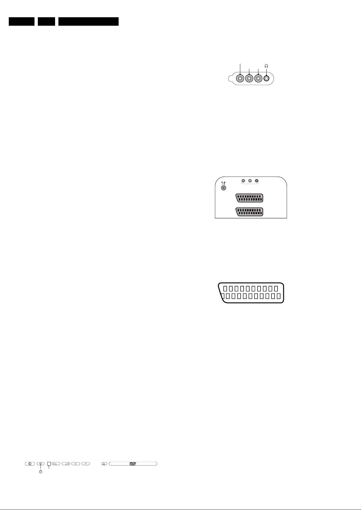
1.2 Connections / Control Facilities
1.2.1 Side Connections and Front Control
-
+
IR
Figure 1-1 Front Control
F_15160_001.eps
040705
F_15160_002.eps
040705
Figure 1-2 Side AV
Audio / Video In
1 -Video CVBS (1 Vpp / 75 Ω) jq
2 -Audio L (0.5 Vrms / 10 kΩ) jq
3 -Audio R (0.5 Vrms / 10 kΩ) jq
4 -Headphone 3.5 mm (8 - 600 Ω / 4 mW) rt
1.2.2 Rear Connections
AUDIO
LR
PCM
AV OUT
EXT2
EXT1
F_15160_003.eps
040705
Figure 1-3 Rear Connections
TV Aerial In
Aerial input : 75 Ω, Coax (IEC-type)
External 1: RGB in + CVBS in/out
21
20
E_06532_001.eps
2
1
050404
Figure 1-4 SCART connector
1 -Audio R (0.5 Vrms 10 kΩ k
2 -Audio R (0.5 Vrms 10 kΩ j
3 - Audio L (0.5 Vrms 1 kΩ k
4 - GND H
5 - GND H
6 - Audio L (0.5 Vrms 10 kΩ j
7 - Blue (0.7 Vpp / 75 Ω) j
8 - CVBS-status 0 - 2.0 V: INT
4.5 - 7 V: EXT 16:9
9.5 - 12 V: EXT 4:3
9 - GND H
10 -
11 - Green (0.7 Vpp / 75 Ω) j
12 -
13 - GND H
14 - GND H
15 - Red (0.7 Vpp / 75 Ω) j
16 - RGB-status 0 - 0.4 V: INT
1 - 3 V: EXT / 75 Ω
17 - GND H
18 - GND H
19 - CVBS (1 Vpp / 75 Ω) k
20 - CVBS (1 Vpp / 75 Ω) j
21 - Earth GND vj
Page 3
Technical Specifications, Connections and Chassis Overview
EN 3TDVD3.1E AA 1.
External 2: CVBS in/out
1 - Audio R (0.5 Vrms 10 kΩ k
2 - Audio R (0.5 Vrms 10 kΩ j
3 - Audio L (0.5 Vrms 1 kΩ k
4- GND H
5- GND H
6 - Audio L (0.5 Vrms 10 kΩ j
7-
8 - CVBS-status 0 - 2.0 V: INT
4.5 - 7 V: EXT 16:9
9.5 - 12 V: EXT 4:3
9- GND H
10 -
11 -
12 -
13 - GND H
14 - GND H
15 -
16 -
17 - GND H
18 - GND H
19 - CVBS (1 Vpp / 75 Ω) k
20 - CVBS (1 Vpp / 75 Ω) j
21 - Earth GND j
1.2.3 DVD Module Connections
DC Power Connector (CN1)
1. Supply voltage + 12 V
2. Ground GND
3. Supply voltage + 3.3 V
4. Ground (analogue) A-GND
5. Ground (digital) D-GND
6. Supply voltage + 5 V
7. Power Control Active high
A/V and DAIC Output (CN6)
1. R/R (PCM3) Rear Right Audio (Audio Data 3)
2. AGND Audio Ground _
3. R/L (PCM2) Rear Left Audio (Audio Data 2)
4. CEN (PCM1) Centre Audio (Audio Data 1)
5. A-GND Audio Ground
6. S/W (PCM0) Sub Woofer (Audio Data 0)
7. F/R (SCK) Front Right Audio (System clock)
8. AGND Audio Ground
9. F/L (BCK) Front Left Audio (Audio bit clock)
10. MUTE (LRCK) Mute for Audio (Audio L/Rch clock)
11. SPDIF Digital Audio
12. D-GND Digital Ground
13. CVBS 1 Vpp / 75 Ohm
14. VGND Video Ground
15. Y 1 Vpp / 75 Ohm
16. VGND Video Ground
17. C 0.3 Vpp / 75 Ohm
18. VGND Video Ground
19. G(Y) 0.7 Vpp / 75 Ohm
20. B(Cb) 0.7 Vpp / 75 Ohm
21. R(Cr) 0.7 Vpp / 75 Ohm
22. VGND Video Ground
23. VID_S/W Video switching
24. TV_S/W TV switching
25. MODE1 SCL or TXD
26. MODE2 SDA or RXD
Slave Interface Connector (CN7)
1. INTOR
2. GND
3. VDATAIN
4. VDATAOUT
5. VCLK
6. VSTB
External A/V Interface Connector(CN8)
1. POWER
2. STOP
3. EJECT
4. LED1
5. NEXT
6. BACK
7. PLAY
8. LED2
9. EXT_IF_!
10. EXT_IN_2
11. Ground
1.3 Chassis Overview
CRT PANEL
A13
KEYBOARD PANEL
A11
SIDE AV PANEL
A8
LINE OUT PANEL
A15
Figure 1-5 Chassis Overview
MAIN
CHASSIS
PANEL
DVD ENGINE
TUNER
MCU & EEPROM
SOUND
DEFLECTION
VIDEO
DVD AV
POWER SUPPLY
SCART
EJECT
A1
A2
A3
A4
A5
A6
A9
A10
A14
F_15160_054.eps
250805
Page 4

EN 4 TDVD3.1E AA2.
Safety Instructions, Warnings, and Notes
2. Safety Instructions, Warnings, and Notes
Index of this chapter:
2.1 Safety Instructions
2.2 Warnings
2.3 Notes
2.1 Safety Instructions
Safety regulations require the following during a repair:
• Connect the set to the Mains (AC Power) via an isolation
transformer (> 800 VA).
• Replace safety components, indicated by the symbol h,
only by components identical to the original ones. Any
other component substitution (other than original type) may
increase risk of fire or electrical shock hazard.
Safety regulations require that after a repair, the set must be
returned in its original condition. Pay in particular attention to
the following points:
• Route the wire trees correctly and fix them with the
mounted cable clamps.
• Check the insulation of the Mains (AC Power) lead for
external damage.
• Check the strain relief of the Mains (AC Power) cord for
proper function.
• Check the electrical DC resistance between the Mains (AC
Power) plug and the secondary side (only for sets that have
a Mains (AC Power) isolated power supply):
1. Unplug the Mains (AC Power) cord and connect a wire
between the two pins of the Mains (AC Power) plug.
2. Set the Mains (AC Power) switch to the "on" position
(keep the Mains (AC Power) cord unplugged!).
3. Measure the resistance value between the pins of the
Mains (AC Power) plug and the metal shielding of the
tuner or the aerial connection on the set. The reading
should be between 4.5 Mohm and 12 Mohm.
4. Switch "off" the set, and remove the wire between the
two pins of the Mains (AC Power) plug.
• Check the cabinet for defects, to prevent touching of any
inner parts by the customer.
2.3 Notes
2.3.1 General
• Measure the voltages and waveforms with regard to the
chassis (= tuner) ground (H), or hot ground (I), depending
on the tested area of circuitry. The voltages and waveforms
shown in the diagrams are indicative. Measure them in the
Service Default Mode (see chapter 5) with a colour bar
signal and stereo sound (L: 3 kHz, R: 1 kHz unless stated
otherwise) and picture carrier at 475.25 MHz for PAL, or
61.25 MHz for NTSC (channel 3).
• Where necessary, measure the waveforms and voltages
with (D) and without (E) aerial signal. Measure the
voltages in the power supply section both in normal
operation (G) and in stand-by (F). These values are
indicated by means of the appropriate symbols.
• The semiconductors indicated in the circuit diagram and in
the parts lists, are interchangeable per position with the
semiconductors in the unit, irrespective of the type
indication on these semiconductors.
2.3.2 Schematic Notes
• All resistor values are in ohms, and the value multiplier is
often used to indicate the decimal point location (e.g. 2K2
indicates 2.2 kohm).
• Resistor values with no multiplier may be indicated with
either an "E" or an "R" (e.g. 220E or 220R indicates 220
ohm).
• All capacitor values are given in micro-farads (µ= x10
nano-farads (n= x10
• Capacitor values may also use the value multiplier as the
decimal point indication (e.g. 2p2 indicates 2.2 pF).
• An "asterisk" (*) indicates component usage varies. Refer
to the diversity tables for the correct values.
• The correct component values are listed in the Spare Parts
List. Therefore, always check this list when there is any
doubt.
-9
), or pico-farads (p= x10
-12
-6
),
).
2.2 Warnings
• All ICs and many other semiconductors are susceptible to
electrostatic discharges (ESD w). Careless handling
during repair can reduce life drastically. Make sure that,
during repair, you are connected with the same potential as
the mass of the set by a wristband with resistance. Keep
components and tools also at this same potential. Available
ESD protection equipment:
– Complete kit ESD3 (small tablemat, wristband,
connection box, extension cable and earth cable) 4822
310 10671.
– Wristband tester 4822 344 13999.
• Be careful during measurements in the high voltage
section.
• Never replace modules or other components while the unit
is switched "on".
• When you align the set, use plastic rather than metal tools.
This will prevent any short circuits and the danger of a
circuit becoming unstable.
2.3.3 Rework on BGA (Ball Grid Array) ICs
General
Although (LF)BGA assembly yields are very high, there may
still be a requirement for component rework. By rework, we
mean the process of removing the component from the PWB
and replacing it with a new component. If an (LF)BGA is
removed from a PWB, the solder balls of the component are
deformed drastically so the removed (LF)BGA has to be
discarded.
Device Removal
As is the case with any component that, is being removed, it is
essential when removing an (LF)BGA, that the board, tracks,
solder lands, or surrounding components are not damaged. To
remove an (LF)BGA, the board must be uniformly heated to a
temperature close to the reflow soldering temperature.
A uniform temperature reduces the risk of warping the PWB. To
do this, we recommend that the board is heated until it is certain
that all the joints are molten. Then carefully pull the component
off the board with a vacuum nozzle. For the appropriate
temperature profiles, see the IC data sheet.
Area Preparation
When the component has been removed, the vacant IC area
must be cleaned before replacing the (LF)BGA.
Removing an IC often leaves varying amounts of solder on the
mounting lands. This excessive solder can be removed with
either a solder sucker or solder wick. The remaining flux can be
removed with a brush and cleaning agent.
Page 5
Safety Instructions, Warnings, and Notes
EN 5TDVD3.1E AA 2.
After the board is properly cleaned and inspected, apply flux on
the solder lands and on the connection balls of the (LF)BGA.
Note: Do not apply solder paste, as this has been shown to
result in problems during re-soldering.
Device Replacement
The last step in the repair process is to solder the new
component on the board. Ideally, the (LF)BGA should be
aligned under a microscope or magnifying glass. If this is not
possible, try to align the (LF)BGA with any board markers.
So as not to damage neighbouring components, it may be
necessary to reduce some temperatures and times.
More Information
For more information on how to handle BGA devices, visit this
URL: www.atyourservice.ce.philips.com (needs subscription,
not available for all regions). After login, select “Magazine”,
then go to “Workshop Information”. Here you will find
Information on how to deal with BGA-ICs.
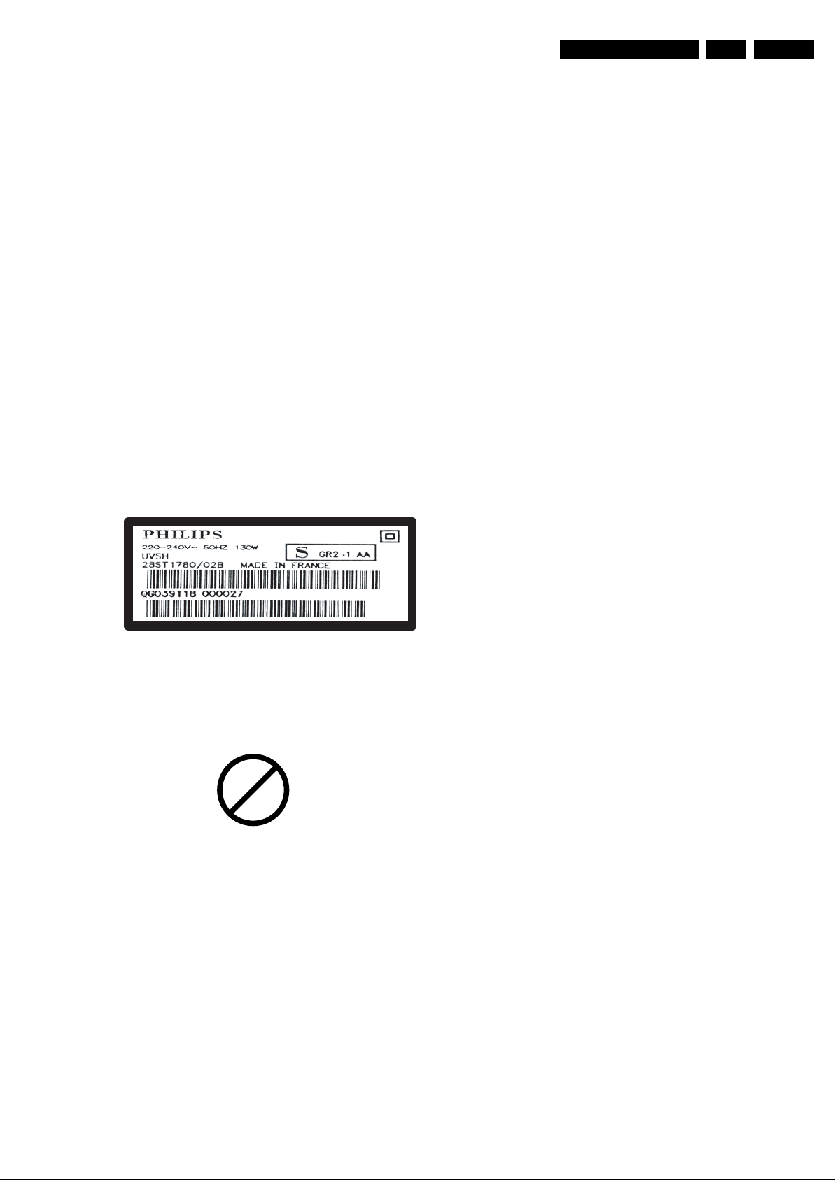
2.3.4 Lead-free Solder
Philips CE is producing lead-free sets (PBF) from 1.1.2005
onwards.
Identification: The bottom line of a type plate gives a 14-digit
serial number. Digits 5 and 6 refer to the production year, digits
7 and 8 refer to production week (in example below it is 1991
week 18).
To avoid wear-out of tips, switch “off” unused equipment or
reduce heat.
• Mix of lead-free soldering tin/parts with leaded soldering
tin/parts is possible but PHILIPS recommends strongly to
avoid mixed regimes. If this cannot be avoided, carefully
clear the solder-joint from old tin and re-solder with new tin.
• Use only original spare-parts listed in the Service-Manuals.
Not listed standard material (commodities) has to be
purchased at external companies.
• Special information for lead-free BGA ICs: these ICs will be
delivered in so-called "dry-packaging" to protect the IC
against moisture. This packaging may only be opened
shortly before it is used (soldered). Otherwise the body of
the IC gets "wet" inside and during the heating time the
structure of the IC will be destroyed due to high (steam-)
pressure inside the body. If the packaging was opened
before usage, the IC has to be heated up for some hours
(around 90°C) for drying (think of ESD-protection!).
Do not re-use BGAs at all!
• For sets produced before 1.1.2005, containing leaded
soldering tin and components, all needed spare parts will
be available till the end of the service period. For the repair
of such sets nothing changes.
In case of doubt whether the board is lead-free or not (or with
mixed technologies), you can use the following method:
• Always use the highest temperature to solder, when using
SAC305 (see also instructions below).
• De-solder thoroughly (clean solder joints to avoid the
mixing of two alloys).
E_06532_024.eps
230205
Figure 2-1 Serial number example
Regardless of the special lead-free logo (which is not always
indicated), one must treat all sets from this date onwards
according to the rules as described below.
P
b
Figure 2-2 Lead-free logo
Due to lead-free technology some rules have to be respected
by the workshop during a repair:
• Use only lead-free soldering tin Philips SAC305 with order
code 0622 149 00106. If lead-free solder paste is required,
please contact the manufacturer of your soldering
equipment. In general, use of solder paste within
workshops should be avoided because paste is not easy to
store and to handle.
• Use only adequate solder tools applicable for lead-free
soldering tin. The solder tool must be able:
– To reach a solder-tip temperature of at least 400°C.
– To stabilise the adjusted temperature at the solder-tip.
– To exchange solder-tips for different applications.
• Adjust your solder tool so that a temperature of around
360°C - 380°C is reached and stabilised at the solder joint.
Heating time of the solder-joint should not exceed ~ 4 sec.
Avoid temperatures above 400°C, otherwise wear-out of
tips will increase drastically and flux-fluid will be destroyed.
Caution: For BGA-ICs, you must use the correct temperature
profile, which is coupled to the 12NC. For an overview of these
profiles, visit the website www.atyourservice.ce.philips.com
(needs subscription, but is not available for all regions).
You will find this and more technical information within the
"Magazine", chapter "Workshop information".
For additional questions please contact your local repair help
desk.
2.3.5 Practical Service Precautions
• It makes sense to avoid exposure to electrical shock.
While some sources are expected to have a possible
dangerous impact, others of quite high potential are of
limited current and are sometimes held in less regard.
• Always respect voltages. While some may not be
dangerous in themselves, they can cause unexpected
reactions that are best avoided. Before reaching into a
powered TV set, it is best to test the high voltage insulation.
It is easy to do, and is a good service precaution.
Page 6

EN 6 TDVD3.1E AA3.
3. Directions for Use
You can download this information from the following websites:
http://www.philips.com/support
http://www.p4c.philips.com
Directions for Use
Page 7
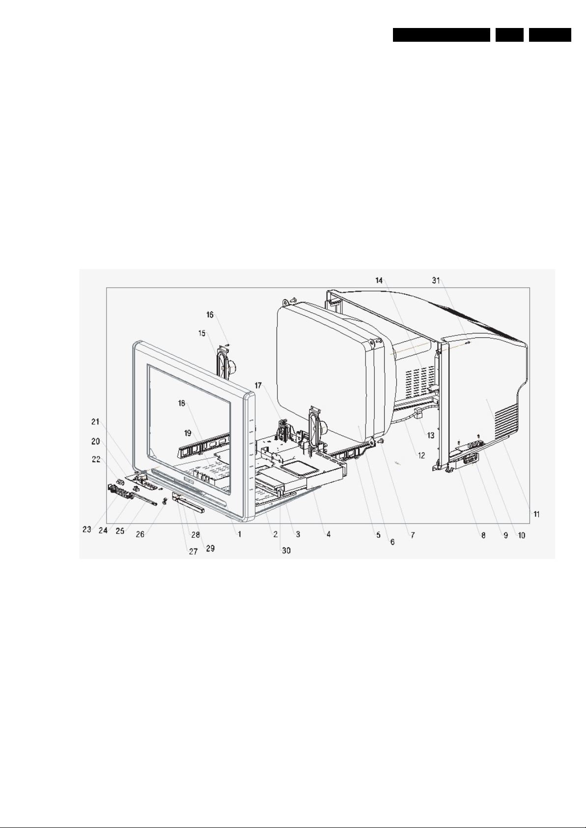
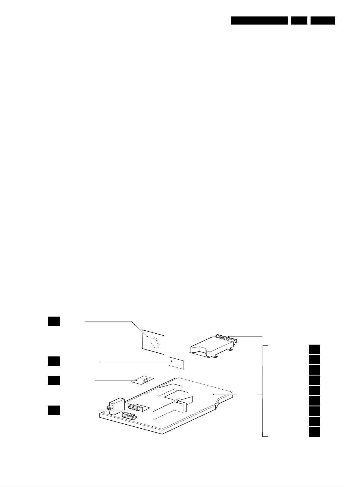
4. Mechanical Instructions
Index of this chapter:
4.1 Exploded View
4.2 Rear Cover Removal
4.3 Service Position Main Panel
4.4 DVD Module Removal
4.5 Side I/O Panel Removal
4.6 Rear I/O Panel Removal
4.7 Rear Cover Mounting
Notes:
• Figures below can deviate slightly from the actual situation,
due to the different set executions.
• Follow the disassemble instructions in described order.
4.1 Exploded View
Mechanical Instructions
EN 7TDVD3.1E AA 4.
4.2 Rear Cover Removal
1. Remove all fixation screws (4x) of the rear cover.
2. Pull the rear cover a little backwards.
3. Disconnect the Rear I/O panel
4. Now pull the rear cover backwards to remove it.
4.3 Service Position Main Panel
1. Disconnect all cables of the DVD module
2. Remove the main panel [1]. At the same time, pull the
panel away from the
3. CRT [2].
4. Turn the panel 90 degrees clockwise [3].
5. Flip the panel 90 degrees [4], with the components towards
6. the CRT.
Figure 4-1 Exploded view
4.4 DVD Module Removal
4.5 Side I/O Panel Removal
4.6 Rear I/O Panel Removal
F_15160_013.eps
040705
Remove the complete DVD module after unscrewing the four
fixation screws [1].
Remove the side I/O panel after unscrewing the screws (2x) at
the bottom of the set.
Remove the rear I/O panel after unscrewing the two screws
from the inside of the rear cover.
Page 8

EN 8 TDVD3.1E AA4.
4.7 Rear Cover Mounting
To reassemble the set, perform all described processes in
reverse order.
Be sure that, before the rear cover is mounted:
• The mains cord is mounted correctly in its guiding bracket.
• All wires/cables are returned in their original position
Mechanical Instructions
Page 9

Service Modes, Error Codes and Fault Finding
5. Service Modes, Error Codes and Fault Finding
EN 9TDVD3.1E AA 5.
Index of this chapter
5.1 Service Modes
5.2 Fault Finding and Repair Tips
5.1 Service Modes
The Service Mode is a combination of the TV Service Mode
and the DVD Service Mode. You can enter the DVD Service
Mode via the TV Service Mode. The Service Mode offers
features, which the service technician can use to repair a set.
Any feature change, made via the Service Menu, will respond
at the same time The Dealer Mode is a special DVD mode, to
provide an auto replay function for commercial purposes. All
displayed text strings in the Service Modes are in English.
5.1.1 TV Service Mode
Purpose
• To perform alignments (e.g. colour adjustment and
geometry alignments)
• To change option settings
• DVD Service menu
Specifications
All service unfriendly modes (if present) are disabled, like:
• Auto switch 'off' (when there is no 'ident' signal)
• Timer switch to a channel
• Automatic user menu time-out
• The NVM is unprotected
• AV functions are not working
How to Enter the Service Mode
Screen menu's must be 'off', when you enter the Service Mode.
Use a standard customer RC transmitter and key in the code
062596 directly followed by the MENU button in 10 seconds.
The following screen is visible when you enter the Service
Mode:
ST92195PWS7-V3 06.06.05
Program 06
OPTIONS
GEOMETRY
G2A
VIDEO
TUNER/IF
DVD
F_15160_005.eps
Figure 5-1 Figure 5.1 TV Service Mode Menu.pdf
• LLLLLLL. This is the used IC type.
• PAB#-XX. This is the software identification.
– P = Philips.
– A = the region (W = West Europe, E = East Europe).
– B = sound specification (M = Mono, S = Stereo).
– # = number of TXT pages.
– XX = the software version number (the first X is the
main software version number and the second X is the
sub software version number).
• PROGRAM. .......
• OPTIONS. Three codes possible.
• GEOMETRY. To align the geometry (see chapter 8.x for a
detailed description).
• G2A. To align the G2 (see chapter 8.x for a detailed
description).
• VIDEO. To adjust RGB, R_cut-off and G_cut-off.
• TUNER/IF. To align the tuner.
• DVD. To enter the DVD Service Mode.
How to Navigate
• Select menu items with the CURSOR UP/DOWN keys.
• With the CURSOR LEFT/RIGHT keys, it is possible to
change the value of the first item (Program)
• With the CURSOR RIGHT and OK keys, activate the
selected menu item.
• When you press the MENU key in a sub menu, you will
return to the previous menu.
• When you press the MENU key in the Service Mode menu,
you will return to the Main menu.
How to Exit
• With the STANDBY command, the set switches to
Standby.
• With the MENU key, the set returns to the Main menu.
Switching the set 'off' and 'on' with the mains switch, brings
the set into normal operation again. All changes in the
Service Mode are stored immediately.
5.1.2 Dealer Mode
Purpose
• To provide an auto replay function (commercial purpose).
• To ignore some features.
Pre-conditions to Start the Dealer Mode are:
• Put the set in DVD Mode (not necessary but is better).
• Switch Teletext 'off' (if set is in TV Mode).
• Switch Childlock 'off'.
• No screen Menu's.
• A DVD disc is present in the tray.
• Close disc tray.
• Switch the DVD in PLAY condition.
Specifications
• The information line displays the current mode.
• The set starts to play the disc.
• The Disc Menu passes automatically.
• At the end of the disc, the set replays the disc from chapter
1 onwards.
In Dealer Mode, some restrictions and rules are defined:
• While the Dealer Mode is active, you cannot use the
STANDBY key (RC reception is blocked), so it is not
possible to go to standby. The only way to switch off
the set is to switch the Mains Power 'off'.
• When the mains Power is switched 'on', the set will go out
of standby (DVD Mode) automatically.
250805
How to Enter the Dealer Mode
Use a standard RC-transmitter and key in the code 9999
directly followed by the MENU button.
The set will now switch to Dealer Mode. The current mode is
written to the
NVM.
The set switches to the DVD mode and informs the DVD about
the current mode
Dealer Mode ON
F_15160_006.eps
040705
Figure 5-2 Figure 5.2 Dealer Mode menu
Page 10
EN 10 TDVD3.1E AA5.
Service Modes, Error Codes and Fault Finding
How to Exit
Use a standard RC-transmitter and key in the code 9999
directly followed by the MENU button.
5.2 Fault Finding and Repair Tips
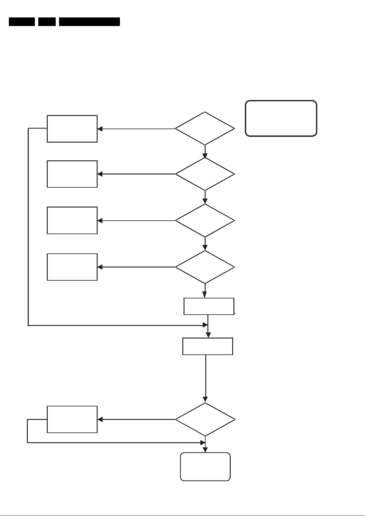
5.2.1 Fault Tracing Diagram for Power Supply
D101-04
C101-04
C106, T101
R107, R105
open
circuit
YES
NO
The Play mode is stopped, the Dealer mode is deactivated, and
the TV menu -Returns
Switched mode
Power Supply defective,
Fuse
F1
Defective
+123V is missing or
level is wrong
NO
Voltag e at
drain of
T101
YES
R104
R111, D107
D116,
YES
YES
Voltag e at
I101 pin 3
< 1V
NO
start-up
voltage pin
8
< 8V
NO
I101
NO
Measure
V102, R159
NO
adjustable with
Control range of
switched-mode
Power Supply
Figure 5-3 Fault Tracing
+123V
V101
YES
F_15160_007.eps
040705
Page 11
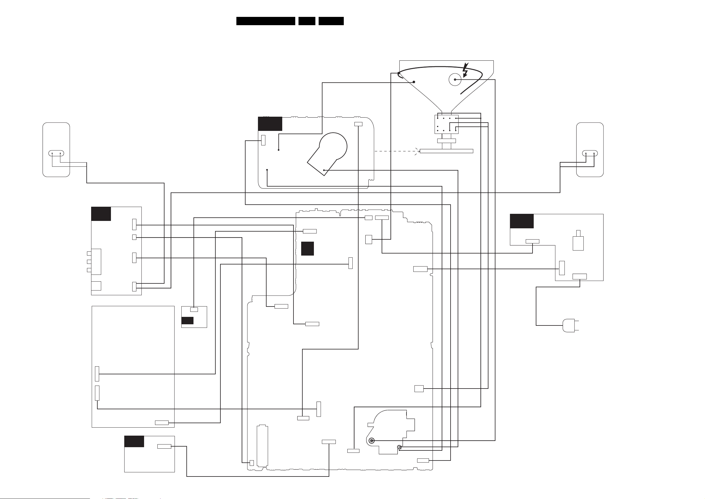
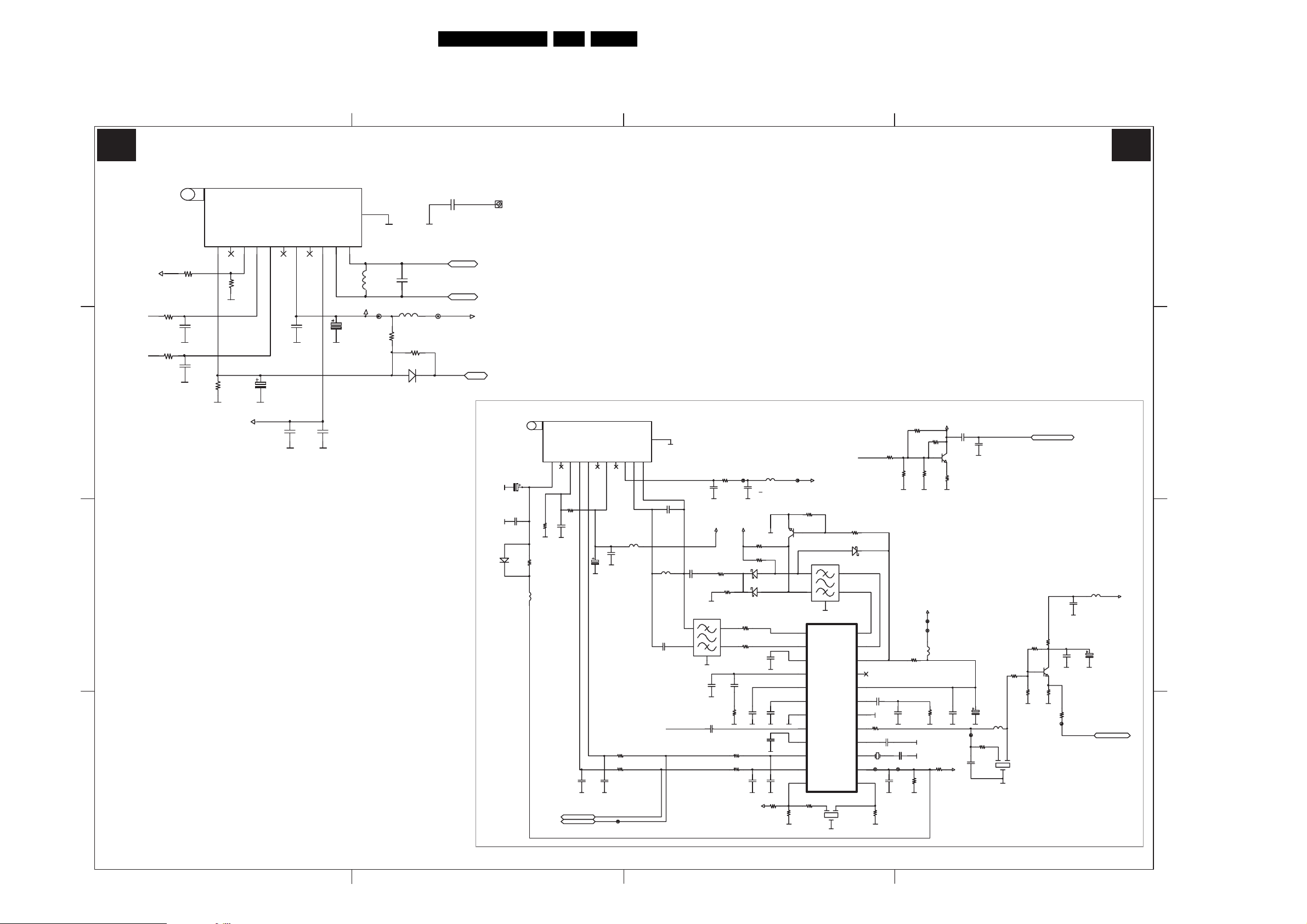
Block Diagrams and Test Point Overviews
6. Block Diagrams and Test Point Overviews
Wiring Diagram
11TDVD3.1E AA 6.
DEGAUSSING COIL
AQUADAG
CRT
EHT
CRT
RIGHT
SPEAKER
VIDEO (YELLOW)
AUDIO LEFT (WHITE)
AUDIO RIGHT (RED)
HEADPHONE
A8
SIDE A/V
K901
K1
K907
K905
S104
4P
S501
5P
S003
2P
S102
2P3
S001
6P
S101
2P3
CRT PANEL
A11
MAINS SWITCH +
KEYBOARD + LED
0214
6P
O212
2P3
LEFT
SPEAKER
MAINS
SWITCH
O211
2P3
A13
S502
4P3
S505
5P
1P
5P
4P
CRT PANEL
S507
S002
A
S506
6P
CRT
SOCKET
MONO
CARRIER
6P
12P
DVD PLAYER
A14
LINE OUT
4P
5P
KS01
A14
2P
0220
EJECT
S202
5P
S302
5P
S403
2P3
JP01
12P
5P
S301
LOT
S303
5P
TUNER
K1
1P
2P
S421
4P3
S401
MAINS
CORD
F_15160_055.eps
290905
Page 12
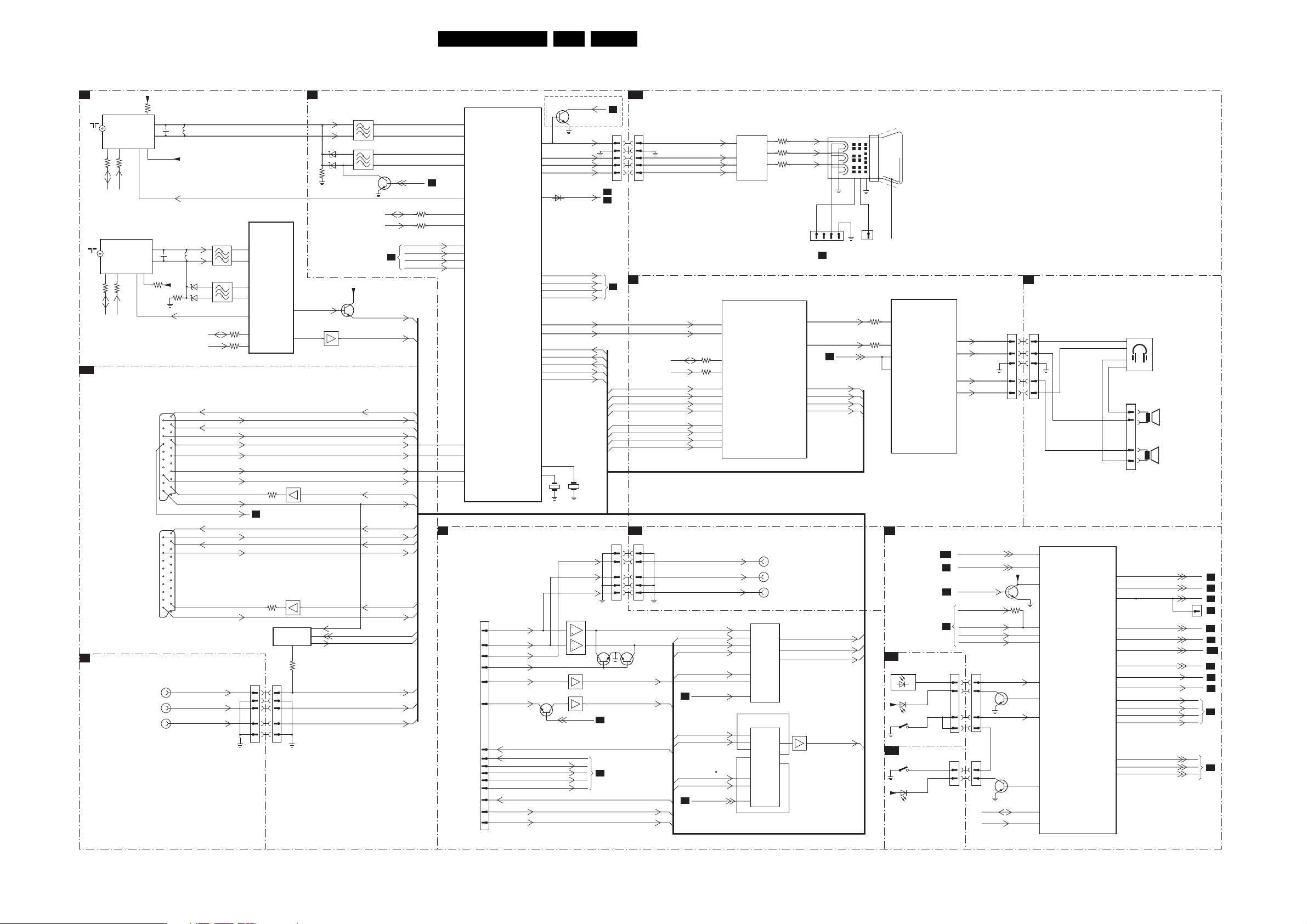
Block Diagrams and Test Point Overviews
Block Diagram Video, Audio, and Control
Video Audio Control
A1
TUNER
X101
UV1316
SDA
54 1
R614
SDA
TT01
UV1316
SDA
54 1
RT09
SDA
A10
SCART
A8
SIDE A/V
MAIN
TUNER
SCL
R613
SCL
TUNER - II
SCL
RT07
SCL
SCART II
AUDIO IN L
AUDIO IN R
AGC
SCART I
VIDEO IN
5VM
RT03
11
1F1
C605
L602
10
1F2
AGC
NC
9
1F1
1F2
9
11
10
RES
RT17
S306A
2
6
8
16
20
S306B
2
6
20
K904
K903
K902
CT13
1
3
7
11
15
19
1
3
19
33V
RT40
33V
AGC
LT04
DT02
DT03
AGC
FRONT_CVBS
FT02
125
FT01
125
SDA
SCL
R1OUT
R1IN
L1OUT
L1IN
FBEXT
EXT1IN
AV_STATUS
R2OUT
SC2_R
L2OUT
SC2_L
EX2_IN
L2IN
R2IN
B
G
R
4
4
RT08
RT10
1T01
TDA9886
DEMODULATOR
6
PIFIN1
7
PIFIN2
1
NC/SIF1
2
NC/SIF2
8
AGCTU
52
SDA
51
SCL
A4
K
901
11
22
33
44
55
IF-PLL
R380
RE11
S302
AUD
CVBS
RES
T310
EF
Q029
EF
CONTROL
R351
8
17
A5
VIDEO PROCESSOR
IF1
1
IF2
2
D307
D308
R345
+5V
Q027
Q030
EF
EXT1IN
AV1/AV2
CVBSEXT
MONO-IN
F301
F302
124
AUDIO_TUNER2
CVBS_TUNER2
FRONT_CVBS
5
4
5
T303
SDA
SCL
A2
R1OUT
R1IN
L1IN
FBEXT
CVBSOUT
EXT1IN
R2OUT
SC2_R
L2OUT
SC2_L
CVBS_TXT
EX2_IN
L2IN
R2IN
12TDVD3.1E AA 6.
A13
S501
55
44
33
22
11
A3
sound
A15
KS01
11
22
33
44
55
T202T201
Y_DVD
CHR_DVD
AV2_ AUD L
AV2_AUDR
CRT
AM_MONO
LDVD/SC2L
RDVD/SC2R
AV2_ AUD L
AV2_ AUD R
LINE OUT
A10
A10
A10
A10
A10
A10
A1
SDA
SCL
R1IN
L1IN
L2IN
R2IN
SC
A5
A1
A3
A3
ICATH
RED
GREEN
BLEU
R208
R207
RDVD_GAIN
LDVD_GAIN
DVD/SC2-SEL
A2
FRONT_CVBS
CVBS_TUNER2
S_SEL_1,2,3
A2
47
44
42
41
39
40
37
38
22
21
SC2_R
SC2_L
EXT2_IN
EXT1_IN
EXT2_IN
I202
MSP3411G
ANA_IN1+
MONO_IN
8
I2C_DA
7
I2C_CL
SC1_IN_R
SC1_IN_L
SC2_IN_L
SC2_IN_R
SC3_IN_L
SC3_IN_R
DACM_R
DACM_L
DOUT
LOUT
ROUT
CONTROL
9,10,11
SOUND
PROCESSOR
KC01
KC02
KC03
U001
74VHC4053M
1
Y1
2
Y0
13
X1
12
X0
5
Z0
3
Z1
A,B,C
U002
74VHC4053M
1
Y1
2
Y0
13
X1
12
X0
5
Z0
3
Z1
9
A,B,C
R519
R518
R517
DACM_L
DACM_R
SC1_OUT_R
SC1_OUT_L
SC2_OUT_R
SC3_OUT_L
SPDIF
AUDIO OUT L
AUDIO OUT R
14
X
15
Y
4
Z
Q007
14
X
15
Y
4
Z
BLU
GRN
RED
+175V
123
S502
TO S401
DEFLECTION
25
24
30
31
27
28
DVD_Y/SC2_V
EF
CVBS_COMM_IN
S506
CRT
HT1
HEATER
A4
TV S/L
TV S/R
A4
R1OUT
L1OUT
R2OUT
L2OUT
LDVD/SC2L
RDVD/SC2R
4
VOL
G1
G3
G2
1
EHT
S505
A8
S301
11
22
33
44
55
SIDE A/V
K907
K906
HEADPHONE
K905
1
2
3
4
SPEAKER
RIGHT
SPEAKER
LEFT
I201
TDA7057Q
AUDI O
R203
R202
A10
A10
A10
A10
AMPLIFIER
3
VIN1
8
5
VIN2
1
7
OUT2+
OUT2-
OUT1-
OUT1+
10
11
13
Control
A2
A3
A3
A5
MCU & EEPROM
A11
KEYBOARD +LED
1002
IR
1008
+5V
LED
4x Switch
Keyboard
A14
EJECT
1010
EJECT
1008
+5V
RES
A10
A6
A5
A6
0214
0220
AV_STATUS
DVD/SC2-SEL
CVBS_TXT
VDATAOUT
VDATAOUT
S001
33
44
55
66
S003
44
11
VSTB
VCLK
SDA
SCL
T002
T005
Q030
IR_TV
KEYB
R179
DVD
Opt.
+5V
8
7
39
5
4
6
1
54
56
48
19
20
I001
ST92195
P02
P03
AVCC
P05
P06
P04
P20
P23
P21
P46
SDA
SCL
MICRO
CONTROLLER
P24
P45
P40
P41
P34
P35
P36
VSYNC
HSYNC
BLUE
GREEN
RED
P01
P00
P37
15
16
17
9
CHR-SW
BRST_ON/0FF
DVD_ STB
VOL
STDBY
AV1/ AV2
L/LA
V_OSD
H_OSD
B_OSD
G_OSD
R_OSD
FB_OSD
S_SEL_1
S_SEL_2
S_SEL_4
S104
A6
A9
A9
1
A9
A3
A9
A10
A5
A4
A4
A5
A6
53
47
42
43
14
13
12
41
40
18
FB
10
11
F_15160_057.eps
290905
1301
STV2246C
PIFIN1
PIFIN2
NC/SIF1
NC/SIF2
AGCTU
SDA
SCL
BOSD
GOSD
ROSD
FBOSD
BEXT
GEXT
REXT
FBEXT
JP01
1
3
24
13
10
11
6
15
16
17
18
22
26
27
28
PROCESSOR
VIDEO
LFB/SSC
CVBSOUT
AUDOUT
CVBS3
CVBS2
NTBC/CVBSOUT1
CVBSOUT1
R_DVD
L_DVD
COAX
MUTE_DVD
Y.D V D
C_DVD
AUDIO_TUNER2
VDATAOUT
CVBS_COMM_IN
AV2_AUDL
AV2_AUDR
ICATH
ROUT
GOUT
BOUT
HOUT
VERT
VAMP
CHR
XTAL2
XTAL1
BCL
T315
VDATAIN
6
7
1
2
L/LA
A2
8
R334
R333
B_OSD
G_OSD
R_OSD
FB_OSD
A6
A6
A3
A3
A3
A3
B
G
R
A5
A6
A3
A6
A3
A6
A5
A6
A5
A5
A6
A3
A3
52
51
34
35
36
37
25
26
27
28
A6
DVD + I/O CONNECTIONS
33
32
31
30
46
49
48
47
42
13
55
22
23
20
29
44
39
40
X301
VSTB
VCLK
IR_DVD
D302
BCLG
T314
ICATH
RED
GREEN
BLEU
BCLG
HOSD
HOUT
VERT
V_AMP
AM_MONO
DVD_Y/SC2_V
CHR_DVD
CVBSEXT
CVBS_TXT
CVBSOUT
X302
COAX
L_DVD
R_DVD
I203
LM358N
2
6
T311
EF
T312
EF
CHR_SW
A5
S301
A5
A4
A4
SC
A6
A6
A10
A10,A2
A10
A10
A10
A10
A10
A6
A6
A6
A6
S303
1
7
A2
A2
Page 13
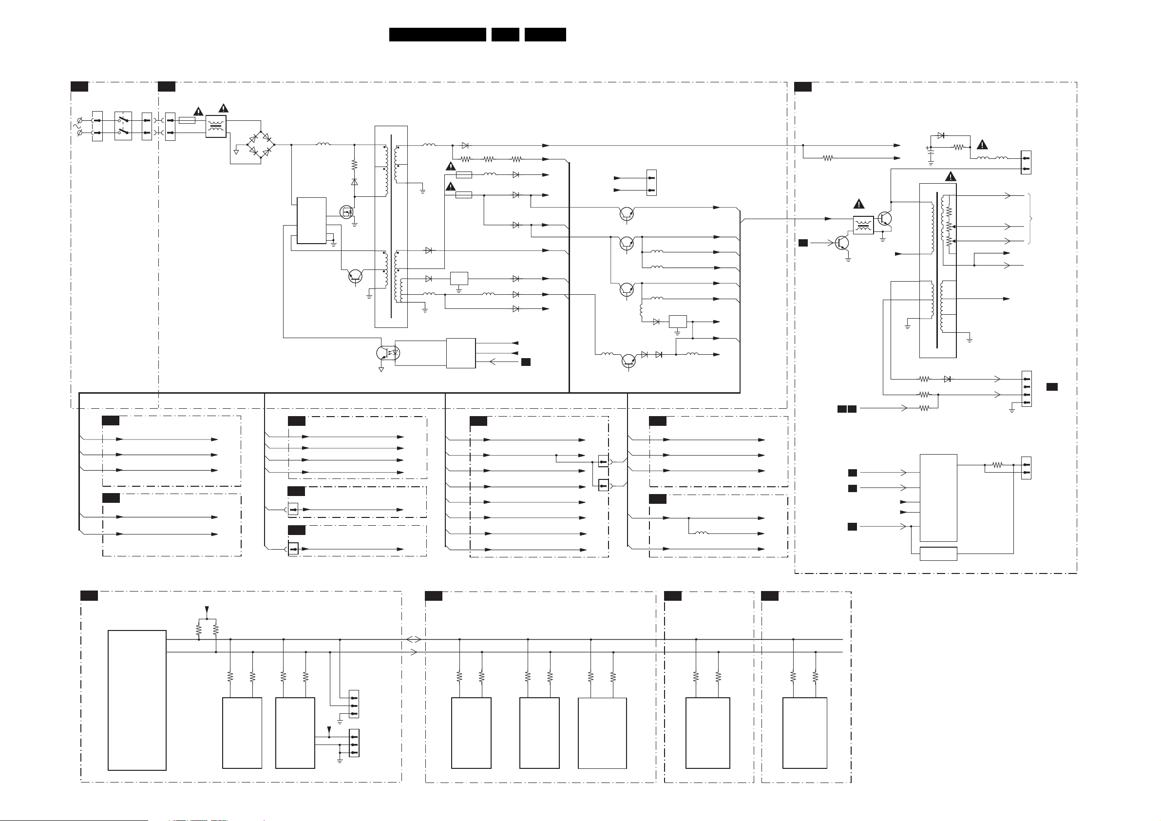
Block Diagrams and Test Point Overviews
Block Diagram Supply, Deflection, and I2C
SUPPLY AND DEFLECTION + I²C
MAIN SWITCH
A11
0211
9002
0212
11
22
DVD + I/O CONNECTIONS
A6
A10
5V
+5V
8V
SCART
+5V
8V
A9
A9
A9
A9
A9
A9
S101
POWER
F101
T2.5A
L101
MAINS
FILTER
5V
+5V
8V
+5V
8V
D102
D103D104
+
-
D101
A9
A9
A9
A9
A2
A2
L111
R110
I101
ICE1QSO1
2
PCS
OUT
4
VCC
SRC
3
GND
RZI
OFC
TUNER
A1
5V
+5V
5VTM
33V
MAIN SWITCH KEYBOARD + LED
A11
0214
+5V
1
EJECT
A14
020
5V
2
D106
T101
7
8
6
5
T115
13TDVD3.1E AA 6.
DEFLECTION
A4
HORIZONTAL DEFLECTION
L110
A9
A9
A9
A9
A9
A9
A9
A9
D108
R115
R167
F3A
R132
F3A
1I02
LM317
IN OUT
ADJ
CONTROL
R135 R136
L114
L006
MCU & EEPROM
A2
5V
+5V
+5VA
+5VD
+5VS
6V5
12(3V3)V
+5VDVDRW
D128
D010
D010
D009
D112
D012
125V
6V5
STDBY
125V
33V
4V5
6V5M
6V5
+16V
8V
+12V
+12VA
A1
+5VDVDRW
A2
A4
A1,A2,A5,A6
A3
4V5
R148
Q001
T105
T108
T110
L117
D122
S104
2
DVD PLAYER
4
L106
L103
L117
D115
D123
To
I105
LF33CV
IN OUT
ADJ
L116
5V
+5V
5VD
5VA
+5VS
+5VDVDRW
+12VDVDRW
+12(3V3)V
+12VDVDRW
A1,A2,A3,A5,A6
A9
A1,A2,A6,A10
A2
A2
A2
A2
A2
R160
16V
T401
HOUT
A5
L401
125V
125VOUT
T402
125VOUT
A4
HOSD
VERTICAL DEFLECTION
V_AMP
V_OSD
VC
+24V_VERT
VERT
5V
+5V
+5VA
+5VD
+5VS
6V5
12(3V3)V
+5VDVDRW
S003
S001
A5
A2
SOUND
A3
A9
A9
2
A14
A9
1
A11
A9
A9
5V
8V
+12V
VIDEO PROCESSOR
A5
5V
8V
L304
5V
8V
+12V
5V
5VC
8V
A5
A2
A5
1
3
11
7
9
5
3
5VTM
2
12
10
4
14
8
16
6
14
I104
TCDT1101G
2
5V
+5V
33V
+5V
5V
L113
D110
D120
L115
C414
L404
HORZ
1
+B
2
5
9
6
R409
R409
R332
I401
TDA1771
4
HEIGHT
2
OSVS
6
RAMPGEN
9
VS
3
TRIGIN
CONTROL
D012
ABL
E/W
12V
D012
OUT
24V
R409
14
13
12
11
8
10
+24V_VERT
4
3
7
HEATER
1
L403
+175V
EHT
FOCUS
BCLG
G2
VC
R428
L402
S403
S401
S421
2
1
1
2
3
4
A
B
TO
HORIZONTOL
DEFLECTION
COIL
TO
CRT
TO S502
A13
CRT BOARD
TO
VERTICAL
DEFLECTION
COIL
I²C
A2
MCU & EEPROM
I001
ST92195
MICRO
CONTROLLER
SDA
SCL
B4D
+5V
R013
R012
19
20
R122
R121
56
U004
PCF8593
LOW POWER
CLOCK
CALENDAR
RES
R049
5
1CO2
24C16
EEPROM
R048
S004
JC01
3
2
1
1
2
3
COMPAIR
SERVICE
CONNECTOR
EXTERNAL
INFRARED
6
+5V
8
7
SDA
SCL
A1
TUNER
R614
54
UV1316
TUNER
X101
MAIN
R613
RT07
RT09
54
TT01
UV1316
TUNER
II
RES
RT08
RT10
11
10
1T01
TDA9886
IF-PLL
DEMODULATOR
RES
A3
SOUND
R208
87
I202
MSP3410G
SOUND
PROCESSOR
R207
VIDEO PROCESSOR
A5
R334
52 51
STV2246C/48C
PROCESSOR
I301
VIDEO
R333
F_15160_056.eps
290905
Page 14
Circuit Diagrams and PWB Layouts
7. Circuit Diagrams and PWB Layouts
Main Panel: Tuner
14TDVD3.1E AA 7.
321
4
A1 A1
TUNER
X101
UV1316
D
C
NUT
GA
2
1
RT04
0R
5VM
RT03
0R
GND-PWR
R613
SCL
100R
C607
100P
GND-PWR
R614
SDA
100R
C608
100P
GND-PWR
C
R602
27K
GND-PWR
B
A
MAIN TUNER
3
1
FHU
FHV
FHV
V5
V5
3
4
5
6
6
GND-PWR
C601
47U25
GND-PWR
33V
GND-PWR
TFA
7
C606
100N
C603
100N
GND-PWR
CN8CN
9
GND-PWR
C627
10N
GND
2FI011FI
C602
100U16
0
GND-PWR
11
L602
1uH
5VM
J995 J257
GND-PWR
C605
8P2
L601
10uH
R601
4K7
R606
15K
D601
LL4148
FOR SECAM L
ELSE D601 JUMPER
IF1
IF2
C260
10N100V
IF1
IF2
AGC
K100
A
5V
AGC
RESERVED
GND-PWR
GND-PWR
D027
LL4148
CT17
47U50
C076
10N
1
R755
10K
GND-PWR
RT22
CHR0805-1R00
LT05
IND500-1U0H
TT01
UV1316
CG
NUT
A
2
GND-PWR
R701
10K
C079
47N
SCL
SDA
II - TUNER
0
GND
LT02
10uH
2FI011FI
11
GND-PWR
CT13
10P
LT04
IND500-1U0H
CT09
1N
MONO-IN
CT08
1N
2
1
GND-PWR
GND-PWR
FT02 K3953M
3
GND-PWR
GND-PWR
CT25
100N
SDA
SCL
RT17
22K
CT01
100N
100N
5V 5V
RT06
1K
RT40
22K
5
4
CT20
390P
RT23
5K6
GND-PWR
RT08
100R
RT10
100R
LT01
J207
10uH
CT02
IND500-10UH
GND-PWR
GND-PWR
RT12
6K8
RT13
6K8
DT02
BA582
DT03
BA582
RT15
0R
RT16
CT11
10N
0R
CT04
100N
GND-PWR
CT12
CT22
10N
470N
GND-PWRGND-PWRGND-PWR
CT10
1N
GND-PWR
CT29
CT28
22P
22P
GND-PWRGND-PWR
RT02
+5V
10K
MONO-IN
33V
J107
RT20
680K
TT02
BC847
FT01 K9453M
1
2
GND-PWR
IT01
1
IF1
2
IF2
3
OP1
4
FMPLL
5
DEEM
6
AFD
7
DGND
8
AUD
9
TOP
10
10
SDA
SDA
11
SCL
12
SIOMAD
TDA9886
RT11
RT39
100R
10K
GND-PWR GND-PWR
3
1
2
GND-PWR
RT21
220K
DT01
BA582
5
4
24
SIF2
23
SIF1
22
DELEAT
21
AFC
20
VP
CT21
19
VPLL
220N
18
AGND
GND-PWR
RT18
17
CVBS
100R
16
VAGC
XT01
15
REF
4MHZ HC49
14
TAGC
13
NC
3
TPW02B
FT03
RT26
12K
RT34
0R
GND-PWR
CT23
470N
GND-PWR
CT06
100N
CT15
10P
J071J070
RT35
0R
CT24
1N5
GND-PWR
RT05
22K
3FHV
1FHV
FHU
3
TFA
C
CN
V5
N
6
4
5V56
7
8
9
CT03
100N
GND-PWR
GND-PWR
CT07
100U50
RT07
100R
RT09
100R
CT27
CT26
47P
47P
GND-PWRGND-PWR
SCL
SDA
J027
RT33
0R
J067
GND-PWR
GND-PWR
RT01
100K
RT28
10K
RT29
10K
+5V
J073
LT03
10uH
GND-PWR
RT14
330R
RT25
12K
GND-PWRGND-PWRGND-PWR
+5V
Q030
BC547B
RT38
390R
GND-PWR
CT33
470N
CT05
100N
5V
GND-PWR
CT34
220N
AUDIO_TUNER2
AUDIO_TUNER2
II - TUNER AUDIO AMPLIFIER
RT32
10K
Q027
RT36
100R
RT30
1K
GND-PWR
FT04
TPW02B
GND-PWR
GND-PWR
J239
CT14
10P
RT24
620R
CT16
10U25
LT07
4.7uH
123
GND-PWR
GND-PWR
RT27
10R
CT30
100N
GND-PWR GND-PWR
BC848BLT1
RT37
220R
RT31
75R
J080
CVBS_TUNER2
CT31
100N
LT06
10uH
IND500-10UH
CT32
10U25
CVBS_TUNER2
D
C
+5V
B
A
1 2 3 4
F_15160_052.eps
250805
Page 15
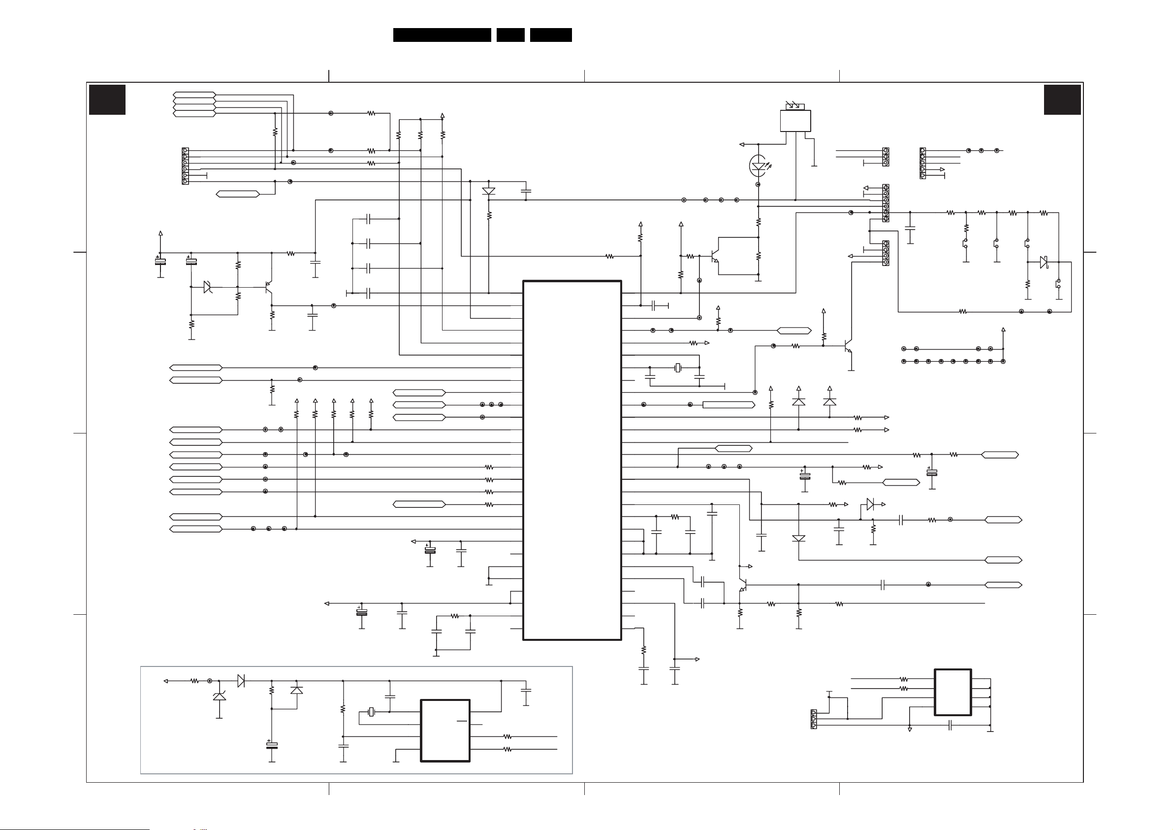
Circuit Diagrams and PWB Layouts
15TDVD3.1E AA 7.
Main Panel: EEPROM
4321
VSTB
A2 A2
MCU & EEPROM
D
VCLK
VDATAOUT
VDATAIN
S002
1
2
3
4
5
6
DVD TV
VDATAIN
GND-PWR
IR_DVD
RW OPT.
R178
0R
J148
J100
J149
VSTB
VCLK
VDATAOUT
IR_DVD
J147
+5V
R011
C006
47U25
GND-PWR
C
B
C001
10U50
R001
220R
GND-PWR
DVD/SC2-SEL
AV_STATUS
L/LA
AV1/AV2
STDBY
B_OSD
G_OSD
R_OSD
SDA
SCL
D003
2.7V ZENER
R055
220R
R064
220R
DVD/SC2-SEL
AV_STATUS
L/LA
AV1/AV2
STDBY
B_OSD
G_OSD
R_OSD
SDA
SCL
J078 J087 J106
100R
GND-PWR
T003
BC858BLT1
R056
4K7
GND-PWR GND-PWR
J998
J112
R043
4K7
GND-PWR
R013
4K7
+5V+5V
R012
4K7
J134 J173
J019 J029J058
J009
J008
J007
C032
22P
GND-PWR
C033
4N7
5VA
D050
6V5
RTC
R120 1K
J241
D052
1N5226B 3.3 V ZENER
LL4148
R124
2K2
D051
LL4148
A
GND-PWR
C045
470U16
SUPERCAP 0.1F
RESERVED
1 2 3 4
J098
R015
4K7
DVD OPT.
R179
0R
R063 0R
R062 0R
C026
22P
C028
22P
C027
22P
C002
22P
R007
4K7
GND-PWR
R123
10K
32.768KHZ HC49S
C043
100N
+5V+5V+5V
R010
4K7
C003
10U50
Y002
GND-PWR
C123
GND-PWRGND-PWRGND-PWR
R035
4K7
S_SEL_1
S_SEL_2
S_SEL_3
FB_OSD
5VD
C008
100N
22P
1
2
3
4
+5VDVDRW
R033
4K7
GND-PWR
GND-PWR
U004
XTAL1
XTAL2
RST
VSS
PCF8593
R034
4K7
C004
100U16
C010
2N2
S_SEL_1
S_SEL_2
S_SEL_3
FB_OSD
GND-PWR
R022
5K6
VDD
INT
SCL
SDA
C005
100N
C009
22P
D006
LL4148
R009
220R
J092 J093
J094
J090
R016
1K
R017
1K
R018
1K
R019
470R
GND-PWR
8
7
R121 100R
6
R122 100R
5
1
1
1
2
2
2
3
3
3
4
4
4
5
5
5
6
6
6
7
7
7
8
8
8
9
9
9
10
10
10
11
11
11
12
12
12
13
13
13
14
14
14
15
15
15
16
16
16
17
17
17
18
18
18
19
19
19
20
20
20
21
21
21
22
22
22
23
23
23
24
24
24
25
25
25
26
26
26
27
27
27
28
28
28
GND-PWR
C034
56P
I001
P20
P20
P20
RESET
RESET
RESET
P07
P07
P07
P06
P06
P06
P05
P05
P05
P04
P04
P04
P03
P03
P03
P02
P02
P02
P01
P01
P01
P00
P00
P00
P37
P37
P37
P36
P36
P36
P35
P35
P35
P34
P34
P34
BLUE
BLUE
BLUE
GREEN
GREEN
GREEN
RED
RED
RED
FB
FB
FB
SDA
SDA
SDA
SCL
SCL
SCL
VCC
VCC
VCC
JTDO
JTDO
JTDO
WSCF
WSCF
WSCF
WSCR
WSCR
WSCR
AVDD3
AVDD3
AVDD3
TEST
TEST
TEST
MCFM
MCFM
MCFM
JTCK
JTCK
JTCK
ST92195
C042
100N
SCL
SDA
MCU
R061
0R
P21
P21
P21
P22
P22
P22
P23
P23
P23
P24
P24
P24
P25
P25
P25
OSCIN
OSCIN
OSCIN
OSCOUT
OSCOUT
OSCOUT
P47
P47
P47
P46
P46
P46
P45
P45
P45
P44
P44
P44
P43
P43
P43
P42
P42
P42
P41
P41
P41
P40
P40
P40
VSYNC
VSYNC
VSYNC
HSYNC
HSYNC
HSYNC
AVCC
AVCC
AVCC
PLLR
PLLR
PLLR
PLLF
PLLF
PLLF
VSS
VSS
VSS
AGND
AGND
AGND
CVBS1
CVBS1
CVBS1
CVBS2
CVBS2
CVBS2
JTMS
JTMS
JTMS
AVDD2
AVDD2
AVDD2
CVBS0
CVBS0
CVBS0
TXCF
TXCF
TXCF
+5VDVDRW
R008
4K7
56
56
56
55
55
55
54
54
54
53
53
53
52
52
52
51
51
51
50
50
50
49
49
49
48
48
48
47
47
47
46
46
46
45
45
45
44
44
44
43
43
43
42
42
42
41
41
41
40
40
40
39
39
39
38
38
38
37
37
37
36
36
36
35
35
35
34
34
34
33
33
33
32
32
32
31
31
31
30
30
30
29
29
29
R023
15K
GND-PWR
C029
GND-PWR
22P
J102 J103
X001
4MHZ
C022
22P
BRST_ON/OFF
R025
5K6
C030
22P
C013
2N2
GND-PWR
+5V
C014
470N
R057
10K
R002
2K2
R030
10K
DVD_STB
J626J627
T002
BC848BLT1
J127
+5V
J125
+5V
C023
22P
BRST_ON/OFF
J129 J130 J131
C020
100N
C019
4N7
GND-PWR
C016
470N
C015
100P
5VA
+5V
R065
10K
J066
GND-PWR
DVD_STB
GND-PWR
J116J117J118J121
IR01
34836
GND-PWR
CHR-SW
J126
GND-PWR
5VA
BC848BLT1
R047
4K7
T001
J122
R059
220R
R040
1K5
JS01
0R
+5V
C031
100P
D013
STDBY
J124
R054
4K7
CCV
CHR-SW
R072
10K
+5V
GND-PWR
GND-PWR
DNG
RI
GND-PWR
D004
LL4148
TXT-SW
D001
LL4148
R058
47K
SDA
SCL
GND-PWR
GND-PWR
IR_TV
KEYB
GND-PWR
+5V
+5V
R024
10K
GND-PWR
+5V
D005
LL4148
R080 10K
R081 10K
C041
R060
10U
4K7
R044
10K
C024
GND-PWR GND-PWR
R053
47K
GND-PWR
3
2
1
JC01
EXT INFRARED
+5V
J164
REC_LED&EJECT
T005
BC848BLT1
R032
4K7
DVD_SB
+5V
470P
SDA
SCL
J291
3
2
1
1
2
3
4
5
6
4
3
2
1
D002
LL4148
S004
COMPAIR
S001
IR&LED
S003
C080
10N
SC01
1
2
3
4
5
SERVICE
GND-PWR
J074J082 J175J176
J182J183 J184J185J186J274J275
J181
12(3V3)V
5VS
R052
10K
+5V
DVD_SB
C025
1U50
GND-PWR
+5V
R045
CD28
470N16V
10K
J011
R027
4K7
C040
470N
EEPROM
+5V
IC02 24C16
5
6
7
8
SDA
SCL
PTC
VDD
R049
100RR048
100R
KEYB
SCL
SDA
5VM
GND-PWR
R003
220R
R028
0R
J075
HOSD
CVBS_TXT
TXT-SW
C011
100N
J114J115
R051
470R
SW01 SW02
CH+ CH-
GND-PWR
R077
5K6
VOL
V_OSD
USS
A2
A1
A0
R004
820R
GND-PWR
VOL
4
3
2
1
GND-PWR
J119
R005
560R
R076
5V
J177
V_OSD
HOSD
CVBS_TXT
1K5
GND-PWR
R006
SW04
VOL+
SW03
F_15160_015.eps
D
1K5
D030
BAT85
VOL-
GND-PWR
J300J301
C
B
A
040705
Page 16

Main Panel: Sound
Circuit Diagrams and PWB Layouts
16TDVD3.1E AA 7.
4321
A3 A3
D
C
SOUND
AV2_AUDR
AV2_AUDL
SCL
SDA
SCL
SDA
AV2_AUDR
AV2_AUDL
J085 J105 J108
5V
J160 J136
TV_S/R
TV_S/L
GND-PWR
R209
47K
J135
C216
470N
5V
R207
R208
C208
10U50
C075
22U50
GND-PWR
100R
100R
C215
470N
C218
1N
GND-PWR
GND-PWR
GND-PWR
C077
22U50
GND-PWR
C207
100N
C209
100N
GND-PWR
C210
100N
GND-PWR
C217
1N
SOUND PROCESSOR
I202 MSP 3411G
1
1
1
NC
NC
NC
2
2
2
AUD_OL_OUT
AUD_OL_OUT
AUD_OL_OUT
3
3
3
D_CTH_OUT_1
D_CTH_OUT_1
D_CTH_OUT_1
4
4
4
D_CTR_OUT_0
D_CTR_OUT_0
D_CTR_OUT_0
5
5
5
ADR_SEL
ADR_SEL
ADR_SEL
6
6
6
STANDBYQ
STANDBYQ
STANDBYQ
7
7
7
I2C_CL
I2C_CL
I2C_CL
8
8
8
I2C_DA
I2C_DA
I2C_DA
9
9
9
I2S_CL
I2S_CL
I2S_CL
10
10
10
I2S_WS
I2S_WS
I2S_WS
11
11
11
I2S_DA_OUT
I2S_DA_OUT
I2S_DA_OUT
12
12
12
I2S_DA_IN1
I2S_DA_IN1
I2S_DA_IN1
13
13
13
ADR_DA
ADR_DA
ADR_DA
14
14
14
ADR_WS
ADR_WS
ADR_WS
15
15
15
ADR_CL
ADR_CL
ADR_CL
16
16
16
DVSUP
DVSUP
DVSUP
17
17
17
DVSS
DVSS
DVSS
18
18
18
I2S_DA_IN2
I2S_DA_IN2
I2S_DA_IN2
19
19
19
NC
NC
NC
20
20
20
RESETQ
RESETQ
RESETQ
21
21
21
DACA_R
DACA_R
DACA_R
22
22
22
DACA_L
DACA_L
23
23
23
24
24
24
25
25
25
26
26
26
DACA_L
VREF2
VREF2
VREF2
DACM_R
DACM_R
DACM_R
DACM_L
DACM_L
DACM_L
DACM_SUB
DACM_SUB
DACM_SUB
J153J139
XTAL_OUT
XTAL_OUT
XTAL_OUT
XTAL_IN
XTAL_IN
XTAL_IN
TESTEN
TESTEN
TESTEN
ANA_IN2+
ANA_IN2+
ANA_IN2+
ANA_IN-
ANA_IN-
ANA_IN-
ANA_IN1+
ANA_IN1+
ANA_IN1+
AVSUP
AVSUP
AVSUP
AVSS
AVSS
AVSS
MONO_IN
MONO_IN
MONO_IN
VREFTOP
VREFTOP
VREFTOP
SC1_IN_R
SC1_IN_R
SC1_IN_R
SC1_IN_L
SC1_IN_L
SC1_IN_L
SC2_IN_R
SC2_IN_R
SC2_IN_R
SC2_IN_L
SC2_IN_L
SC2_IN_L
SC3_IN_R
SC3_IN_R
SC3_IN_R
SC3_IN_L
SC3_IN_L
SC3_IN_L
AGNDC
AGNDC
AGNDC
AHVSS
AHVSS
AHVSS
CAPL_M
CAPL_M
CAPL_M
AHVSUP
AHVSUP
AHVSUP
CAPL_A
CAPL_A
CAPL_A
SC1_OUT_L
SC1_OUT_L
SC1_OUT_L
SC1_OUT_R
SC1_OUT_R
SC1_OUT_R
VREF1
VREF1
VREF1
SC2_OUT_L
SC2_OUT_L
SC2_OUT_L
SC2_OUT_R
SC2_OUT_R
SC2_OUT_R
C245
GND-PWR
C236
3.3U50
C235
100N
C227
100N
C241
56P
C222
22U50
C220
22U50
2P2
C244
2P2
GND-PWR
GND-PWR
GND-PWR
GND-PWR
GND-PWR
GND-PWR
J111
C228
3.3U50
C226
10U50
C223
10U50
L2OUT
R2OUT
GND-PWR
C257
330N
C233
330N
C231
330N
C229
330N
F201
TPSRD 4.43
GND-PWR
L2OUT
R2OUT
R212
75R
R211
0R
C239
10U50
C234
330N
C232
330N
C230
330N
R210
0R
GND-PWR
C238
100N
C224
10U50
R224
100R
AM_MONO
R1IN
L1IN
R2IN
L2IN
RDVD/SC2R
LDVD/SC2L
C225
100N
L1OUT
R1OUT
5V
SC
J077J109 J110
GND-PWR
AM_MONO
R1IN
L1IN
R2IN
L2IN
RDVD/SC2R
LDVD/SC2L
8V
GND-PWR
L1OUT
R1OUT
SC
X201
52
52
52
18.432MHZ
51
51
51
50
50
50
GND-PWR
GND-PWR
GND-PWR
GND-PWR
J234
J233
C242
56P
C240
56P
C221
22U50
C219
22U50
49
49
49
48
48
48
47
47
47
46
46
46
45
45
45
44
44
44
43
43
43
42
42
42
41
41
41
40
40
40
39
39
39
38
38
38
37
37
37
36
36
36
35
35
35
34
34
34
33
33
33
32
32
32
31
31
31
30
30
30
29
29
29
28
28
28
27
27
27
D
C
AUDIO AMPLIFIER
R201
1R
I201
TDA7057Q
GND-PWR
D507
LL4148
1NC.V
1NIV
1CN2
3
C201
1000U25
C206
10U50
GND-PWR
C202
4.7U50
R204
R203
4K7
GND-PWR GND-PWR
L/S_VT
1K
C204
10N
GND-PWR
PUSV
DNGS
2NIV
4
5
6
GND-PWR GND-PWR GND-PWR
GND-PWR
C203
4.7U50
R205
1K
GND-PWR
B
+12VA
C258
R228
22k
T151
BC847B
100uf
A
6V5
R229
100k
1 2 3 4
J200 J201 J202 J203
R227
1K2
16V
VOL
T150
BC847B
VOL
J293 J294 J295
R226
2k
JUMPER
J083 J084
R225
D508
2k
1N4148
GND-PWRGND-PWR GND-PWR
2DNGP
+2TUO
2NC.V
7
8
9
R206
4K7
R202
4K7
C205
10N
R/S_VT
1DNGP
+1TUO
-1TUO
-2TUO
31
21
11
01
S202
5
4
3
2
1
GND-PWR
H.P.
F_15160_016.eps
B
A
040705
Page 17

Circuit Diagrams and PWB Layouts
Main Panel: Vertical Deflection
17TDVD3.1E AA 7.
4321
A4 A4
D
C
DEFLECTION
16V
HOUT
HOUT
C407
100N
GND-PWR GND-PWR
R401
4R7
C401
100U25
GND-PWR
D402
LL4148
C414
1U250
T401
BC639
R402
47K
D406
BYV36C
R413
5K6 3W
R403
100R
C402
10N
GND-PWRGND-PWRGND-PWRGND-PWR
!
C515
270N400V
!
1
2
3
602300033071
C405
100N
C413
1N2KV
L401
L403
150uH
125VOUT
R414
1K
5
0.22R 1/2W
4
125V
D401
BYV36C
R404
L402
56uH
R405
39R
GND-PWR
R160
10R 7W
2
1
GND-PWR
S403
HDY
!
T402
BU508DF
S401
CRT BRD
C403
OPT.
GND-PWR GND-PWR
C419
1U160V
GND-PWR
R407
470K
321
4
GND-PWR
RETAEH
ADNG
V571+
GND-PWR
GND-PWRGND-PWR
C404
6N8 2KV
C408
22U160
C409
10U250
D405
BYV36C
HORIZONTAL DEFLECTION
L404 604200000391
ABL
14
EHT
13
FOCUS
12
G2
11
8
10
4
3
76
GND-PWRGND-PWR
125VOUT
R406
JUMPER
R409
JMP
R332
560R
HORZ
+B
VID
H
GND
1
2
5
E/W
24V
9
12V
GND
!
J218
J292
R410
0.22R
D407
BYV36C
GND-PWR GND-PWR
GND-PWR
C462
100P500V
C411
100N
R421
GND-PWR
1M
R429
2K
R415
2K
C417
100N
GND-PWR GND-PWR
C412
1000U35
R425
750K
C418
100N
R422
1M
J205
R423
1M5
R424
1M5
VC
8V
R412
2K4
R411
7K5
R325
22K
J016
BCLG
BCLG
+24V_VERT
J051
J054
VERTICAL DEFLECTION
J060
HOSD
HOSD
I401 TDA1771
D
C
NEGPMAR
5
C444
TUO.FUB
DNG
6
7
R445
8K2
R446
3K3
R449
4R7
C443
22U50
NI.VNI
8SV9
R448
2K0
R450
0.82R
NEG.BF
01
D441
1N4007
C445
100U50
VC
+24V_VERT
B
VC
GND-PWR
A
F_15160_017.eps
250805
THGIEH
NIGIRT
SVSO
TUO
2
3
C442
4
47N
1
GND-PWR
R428
470R
R447
2K4
J240
2200U25
A
R452 3K3
R457
10K
GND-PWR
R456
180K
Q442
BC337-16
Q443
BC327-16
240J
J047J041
+24V_VERT
R440
220R
R441
2R2
GND-PWR
R444 120KR455 100R
C441
220N
B
VERT
S421
B
V_AMP
V_OSD
VERT
V_AMP
V_OSD
VERT
J043
J046
R454
R453
33K
4K7
T441
BC848BLT1
R458
R451
820R
0R
A
GND-PWRGND-PWR GND-PWR
1 2 3 4
Page 18

Main Panel: Video
Circuit Diagrams and PWB Layouts
18TDVD3.1E AA 7.
4321
A5 A5
D
C
B
VIDEO PROCESSOR
D311
ICATH
7.5V ZENER
AGC
SC
SC
T301
3
42
44MH39PF
1HM
GND-PWR
DVD_Y/SC2_V
DVD_Y/SC2_V
B
G
R
FBEXT
LL 4148
0R OPTIONAL
AGC
J061 J069
1
LC1
LC2
CVBSEXT
CHR_DVD
B
G
R
FBEXT
D310
IF1
IF2
R387
10K
R388
47K
GND-PWR
IF1
IF2
C348
10N
C350
R335
220P
100R
GND-PWR GND-PWR
CVBSEXT
8V
J235
J065
CHR_DVD
L302 8u2
123
C353
22N
1
2
J044
GND-PWR
R361
680R
5V
C343
100P
F303
TPW02B
R389
390K
BCLG
T314
BC848BLT1
F301
K3953
3
GND-PWR
L301
10uH
R307
1K5
BCLG
(PAL I--J1981m)
5
4
C344
4N7
J006
L303
8V
10uH
R308
1K5
J158
R303
120R
GND-PWR
GND-PWR
GND-PWR
GND-PWR
C306
330N
GND-PWR
J045
C307
100U16
C308
100N
GND-PWRGND-PWR
J247
C310
100U16
GND-PWR GND-PWR
C314
1U50
GND-PWR
C301
1U16
C302
10U50
C303
22N
C304
1U50
C349
100N
GND-PWR
C305
1N
C309
100N
C311
100N
C313
1U50
C315
1U50
C345
100N
C318
22N
C319
22N
C320
22N
C312
1U50
J015
R301
150R
J024
5
4
GND-PWR
LC1
LC2
J246
J226
GND-PWR
GND-PWR
1
1
1
2
2
2
3
3
3
4
4
4
5
5
5
6
6
6
7
7
7
8
8
8
9
9
9
10
10
10
11
11
11
12
12
12
13
13
13
14
14
14
15
15
15
16
16
16
17
17
17
18
18
18
19
19
19
20
20
20
21
21
21
22
22
22
23
23
23
24
24
24
25
25
25
26
26
26
27
27
27
28
28
28
3
I301
NC/SIF1
NC/SIF1
NC/SIF1
NC/SIF2
NC/SIF2
NC/SIF2
NC/AGCSIF
NC/AGCSIF
NC/AGCSIF
VREF
VREF
VREF
AGCIF
AGCIF
AGCIF
PIFIN1
PIFIN1
PIFIN1
PIFIN2
PIFIN2
PIFIN2
AGCTU
AGCTU
AGCTU
IFPLL
IFPLL
IFPLL
GNDIF
GNDIF
GNDIF
FMOUT
FMOUT
FMOUT
VCCIF
VCCIF
VCCIF
CVBSOUT
CVBSOUT
CVBSOUT
EXTAUD
EXTAUD
EXTAUD
LC1
LC1
LC1
LC2
LC2
LC2
VCC2
VCC2
VCC2
CVBS1
CVBS1
CVBS1
GND
GND
GND
CVBS2
CVBS2
CVBS2
BS
BS
BS
CVBS3
CVBS3
CVBS3
CHR
CHR
CHR
APR
APR
APR
BEXT
BEXT
BEXT
GEXT
GEXT
GEXT
REXT
REXT
REXT
FBEXT
FBEXT
FBEXT
F302
K9453
1
2
STV2246C/48E
T302
R344
68K
BC848BLT1
NTBC/CVBSOUT1
NTBC/CVBSOUT1
NTBC/CVBSOUT1
R341
10K
FMCAP
FMCAP
FMCAP
AUDOUT
AUDOUT
AUDOUT
GND
GND
GND
VCC
VCC
VCC
SDA
SDA
SDA
SCL
SCL
SCL
SLPF
SLPF
SLPF
LFB/SSC
LFB/SSC
LFB/SSC
HOUT
HOUT
HOUT
VERT
VERT
VERT
BCL
BCL
BCL
VCC1
VCC1
VCC1
CVBSOUT1
CVBSOUT1
CVBSOUT1
GND1
GND1
GND1
VAMP
VAMP
VAMP
CLPF
CLPF
CLPF
XTAL1
XTAL1
XTAL1
XTAL2
XTAL2
XTAL2
XTAL3
XTAL3
XTAL3
FBOSD
FBOSD
FBOSD
ROSD
ROSD
ROSD
GOSD
GOSD
GOSD
BOSD
BOSD
BOSD
ICATH
ICATH
ICATH
ROUT
ROUT
ROUT
GOUT
GOUT
GOUT
BOUT
BOUT
BOUT
R342
10K
GND-PWRGND-PWR
56
56
56
55
55
55
54
54
54
GND-PWR
53
53
53
52
52
52
51
51
51
50
50
50
49
49
49
48
48
48
47
47
47
46
46
46
45
45
45
44
44
44
43
43
43
42
42
42
41
41
41
40
40
40
39
39
39
38
38
38
37
37
37
36
36
36
35
35
35
34
34
34
33
33
33
32
32
32
31
31
31
30
30
30
29
29
29
D307
BA282
D308
BA282
T303
BC848BLT1
R346
22K
J022
J209
J195
R334
100R
R333
100R
J039 J040
GND-PWR
C356
0R
C323
100N
C321
100N
AM_MONO
J023
J026
VERT
R343
10K
GND-PWR
J079J091
SDA
SCL
VERT
X302
GND-PWR
3.579MHZ HC49
J018
C322
100N
R314
47K
8V
R345
2K2
L/LA
J168
AM_MONO
GND-PWR
SDA
SCL
C352
22P
C324
100N
R393
1.2K
C342
1N
L/LA
C336
1U50
R320
1K
IF1
X301
XTAL4.43MHZ
J017
C332
100U16
GND-PWR GND-PWR
GND-PWR
C328
100N
C327
GND-PWR
100U16
GND-PWR
GND-PWR
FB_OSD
J188
R_OSD
G_OSD
B_OSD
R315
1K
R317
150R
R391
1.2K
R322
5K6
R340
10K
R331
2K2
GND-PWR
FB_OSD
R_OSD
G_OSD
B_OSD
R316
150R
R318
150R
C333
100N
R329
8K2
L305
10uH
CVBSOUT
R324
10K
GND-PWR
CVBS_TXT
L304
10uH
D304
LL4148
8V
R330
2K2
C358
470P
GND-PWR
CVBS_TXT
R327
470R
CVBSOUT
V_AMP
C325
4N7
5VC
5V
GND-PWR
GND-PWR
C330
4N7
GND-PWR
D303
LL4148
GND-PWR
J048 J049
C335
4.7U50
GND-PWR
V_AMP
D305
R323
LL4148
27K
C326
1U50
ICATH
GND-PWR
RED
GREEN
BLUE
R328
15K
HOSD
C361
470P
R326
56K
8V
R337
330K
GND-PWR
5
4
3
2
1
HOUT
S301
RGB
GND-PWR
HOSD
D302
LL4148
R336
330K
C331
2.2U50
HOUT
5VC
BCLG
GND-PWR
R312
75R
A
75R
75R
D320
5V1 ZENER
D321
5V1 ZENER
D322
5V1 ZENER
D323
5V1 ZENER
C317
1U50
R310
R311
R309
330K
GND-PWR
D
C
B
A
1 2 3 4
F_15160_018.eps
250805
Page 19

Circuit Diagrams and PWB Layouts
Main Panel: DVD + I/O Conn.
19TDVD3.1E AA 7.
4321
A6 A6
DVD + I/O CONN.
S303
LINE_OUT
21345
S_SEL_1
S_SEL_2
S_SEL_3
DVD VIDEO BUFFER
L309
D
R036
L_DVD
L_DVD
R_DVD
R_DVD
J305
100R
R066
100R
R067
2K2
GND-PWR
GND-PWR
GND-PWR
C383
8.2P
C046
10P
C047
10P
T004
BC848BLT1
R068
2K2
1UH
DVD/SC2-SEL
SC2_L
SC2_R
C366
100N
GND-PWR GND-PWR
DVD/SC2-SEL
GND-PWR
GND-PWR
C048
100N
R069
2K2
R070
2K2
VDATAIN
C
5V
T311
BC848BLT1
R349
150R
R353
47R
Y_DVD
T006
BC848BLT1
GND-PWR
R370
8K2
GND-PWR
R371
10K
C379
47U25
GND-PWR
C367
22P
J096
GND-PWR
DVD_BUFFER&GAIN
B
A
L_DVD
R_DVD
R223
10K
C253
10U50
R215
10K
GND-PWRGND-PWR
3
84
+_VCC
I203A
LM358N
1
2
GND
GND-PWR GND-PWR
C249
R214
1K
R216
0R
C248
10U50
220P
R213
0R
C246
2N20
C247
10U50
(OPTIONAL)
JUMPER
J161
R221
2K2
J146
T202
BC848BLT1
5
5
5
6
6
6
R219
1K
R217
0R
C250
10U50
(OPTIONAL)
JUMPER
LDVD_GAIN RDVD_GAIN
R369
330R
SC2_L
LDVD_GAIN
SC2_R
RDVD_GAIN
EXT2_IN
Y_DVD
Y.DVD
+
_
C252
220P
84
84
84
VCC
GND
R368
100R
J104
C050
100N
J020
J005
J036
J089
GND-PWR
I203B
LM358N
7
7
7
GND-PWRGND-PWR
R220
2K2
C382
10P
J088
6
11
10
9
12
13
2
1
5
3
8
GND-PWR
R218
0R
C254
2N20
COAX
R038
10K
U001
INH
A
B
C
X0
X1
Y0
Y1
Z0
Z1
GND
74VHC4053M
C054
100N
CHR_DVD
R222
10R
C255
10U50
C251
10U50
T201
BC848BLT1
5V
VCC
VEE
J030 J031 J032
EXT2_IN
16
5V
J062 J063
LDVD/SC2L
RDVD/SC2R
DVD_Y/SC2_V
LDVD/SC2L
RDVD/SC2R
DVD_Y/SC2_V
14
X
15
Y
4
Z
EXT2_IN
EXT1IN
FRONT_CVBS
CVBS_TUNER2
EXT1IN
FRONT_CVBS
CVBS_TUNER2
7
5V
BC848BLT1
CHR_DVD
T312
R384
8K2
R385
10K
C381
47U25
T315
BC848BLT1
J081
GND-PWR
CHR-SW
C_DVD
C368
22P
CHR-SW
GND-PWR
R_DVD
L_DVD
VDATAIN
AUDIO_TUNER2
8V
AUDIO_TUNER2
CVBS_TUNER2
Y.DVD
C_DVD
MUTE_DVD
VDATAOUT
VSTB
VCLK
IR_DVD
VDATAIN
VDATAOUT
VSTB
VCLK
IR_DVD
VDATAIN
COAX
CVBS_COMM_IN
AV2_AUDL
AV2_AUDR
AV2_AUDL
AV2_AUDR
J053
J014
J157 J163 J165 J138
J021
J154 J156 J159
J101
J214
J055 J099
J137
J150 J151
C060
10P
J145
C061
10P
S_SEL_1
S_SEL_2
S_SEL_3
R039
10K
C051
100N
GND-PWR
J033 J034 J035
J050
C062
C063
10P
10P
GND-PWR
C073
10U25
R702
10K
C071
10U25
C064
10P
C052
100N
GND-PWR
C074
10U25
+5V+5V+5V
R041
10K
R705
220R
GND-PWR
C065
10P
C053
100N
C072
10U25
R708
220R
C066
10P
R707
220R
R050
220R
R706
220R
C067
10P
R710
220R
GND-PWR
R711
220R
C068
10P
R709
220R
11
10
12
13
C069
10P
6
9
2
1
5
3
8
U002
74VHC4053M
U2
1
2
3
4
VCC
INH
A
B
C
X0
X1
Y0
Y1
Z0
Z1
GND
X
Y
Z
VEE
C055
100N
VIDEO SOURCE_SEL
EXT_2_IN
CVBS_TUNER_2
FRONT_CVBS
EXT1_IN
MAK:DVD OPT.
R713
0R
C056
C057
100P
100P
5V
16
R169
5V
R037
10R
10K
14
15
4
Q007
BC848BLT1
R042
1K
GND-PWR GND-PWR
7
S_SEL1 S_SEL2 S_SEL3
000
001
101
111
MAK:DVD OPT.
R712
0R
MAK:RW_ OPT.
MAK:DVD_ OPT.
R715
0R
C058
100P
R714
0R
C059
100P
C049
100N
GND-PWR
R704
75R
GND-PWR
GND-PWR
J144
CVBS_COMM_IN
R703
1K
JP01
1
1
2
2
3
3
4
4
5
5
6
6
7
7
8
8
9
9
10
10
11
11
12
12
13
13
14
14
15
15
16
16
17
17
18
18
19
19
20
20
21
21
22
22
23
23
24
24
25
25
26
26
27
27
28
28
28pin 1mm FFC connector
C070
10P
.
T
PO DV
D
N
NOC CFF NIP
2
1
D
C
B
A
MUTE_DVD
GND-PWR
GND-PWR
J152 J162J140
1 2 3 4
F_15160_019.eps
040705
Page 20

Main Panel: Side A/V
3
1
2
1
3
2
2
H
2
2
3
F
4
F
7
2
D
D
D
V
5
6
6
DGND
1
2
3
0
F
4
2
F
3
F
2
V
1
SPEAKER
Circuit Diagrams and PWB Layouts
20TDVD3.1E AA 7.
12
4
SIDE A/V
A8 A8
D K904
VIDEO
K90
L
K90
R
C
GND
GN
GN
1
GND
1
GND GND GN
1
L901
FB
C90
10PF
L902
10u
C90
10P
L903
10uH GN
C90
10PF
C90
10PF
GND2 GND
C90
10P
C90
10PF
GND GND
R90
VAL
R91
47K 5
R91
47K
GND
K901
1
2
3
4
SIDE_A
D
C
J902 J90
GND1 GND GND
K906
B
HPH723
2
7
5
4
8
3
1
GND1
L90
10uH
L905
10uH
C91
10P
GND1 GND1 GND1 GND
C911
10PF
C91
10P
C91
10P
R90
VAL
R903
VAL
C909
47uF/50V
C908
47uF/50
GND1
K907
1
2
3
4
5
CON5
K905
1
2
3
4
B
A
F_15160_021.eps
12 3 4
A
250805
Page 21

Circuit Diagrams and PWB Layouts
21TDVD3.1E AA 7.
Main Panel: Power
4321
S101
A9 A9
D
POWER
POW1
POWER SW.
S100
220VAC_IN
P102
PTC 18R
S102
B
A
C
B
R155
15R
GND-PWR
T114
BC557B
R170
A
6V5
R168
1K
10K
220VAC
!
J001
B
A
F101
T2.5AL 250V
J002
R026
3M3
R071
3M3
!
32
P101
1
PTH451A
R138
JUMPER
GND-PWR
R142
R145
100R
1K2
GND-PWR
R148
JUMPER
R150
10K
D129
R149
1K
LL4148
GND-PWR GND-PWR
+12V
C160
1N400V
Z101
TL431CZ1
!
VX1
C101
220N275V
+ceS-ceS
+irP-irP
L101
2*27MH
!
R171
4K7
T108
BD537
C154
100N
D123
1N4007
J057
C113
2.2N400V
D101
1N5062
C103
2.2N400V
D102
1N5062
D117
LL4148
C111
10P
GND-PWR
DVD_SB
C110
1N
R133
150R
R131
150R
C129
47U25
LF33CV
D127
1N4007
C102
220N275V
J302
R101
5R6 5W
2
1
OP01
OPT.
R103
18K
J217
V101
TRISK2KH
6V5 +5V
CP45
22U25
R143
1K2
GND-PWR
T110
BD136
D122
1N4007
T109
BC848BLT1
1
2
3
4
R130
4R7
I105
J286
C145
220P
DVD_SB
NC
PCS
RZI
SRC
R104
47K
R140
6K8
C104
2.2N400V
D103
1N5062
C114
2.2N400V
D104
1N5062
C112
560P
I101
ICE1QS01
R174
39K
T105
BC639
D115
1N4007
niVtuoV
DNG
VCC
OUT
GND
OFC
R111
100R
GND-PWR
D113
LL4148
L116
FB
J204
R113
1M
C165
470P
8
7
6
5
D116
LL4148
C135
100N
D114
5.1V ZENER
L117
DVD_RW_OPT
GND-PWR
GND-PWR
+12VDVDRW
12(3V3)V
L106
10uH
L103
10uH
R105
1M2
C140
15P50V
J190J191J192
L004
DVD_OPT
C147
470U25
!
C106
100U 400V
R116
33R
D107
LL4148
J178
GND-PWR
5VS
+5VDVDRW
6V5M
GND-PWR
GND-PWRGND-PWR
C117
56P
R114
390K
J238
C780
470U25
C148
100N
R107
100R
C109
22U50
D131
18V ZENER
5VD
5VA
8V
C119
8.2N400V
C115
100N
T115
BC548B
4V5
+5VDVDRW
J076
I102 LM317
IN OUT
ADJ
C133
1U50
GND-PWR
R176
220R
DVD_STB
J128
R021
270R
R110
33K5W
D106
600V 1.5A
T101
6N80
R109
4M7
R029
82R
GND-PWR
!
OPTIONAL
J282
C169
100N
Q001
BD537
R031
1K8
!
C116
R175
75R
R117
330R
R118
1K8
R172
220R
R154
10K
GND-PWR
T102
BC848BLT1
C132
100N
L111
FB
C105
33N400V
L112
FB
C108
680P1KV
D132
LL4148
C166
10U50
C155
220P2KV
C151
220P2KV
TCDT1101G
2.2N400V
R152
4M7
!
GND-PWR
DVD_STB
+5VDVDRW
GND-PWR
J288
C170
100N
C175
100U16
C168
100N
0R OPTIONAL
GND-PWRGND-PWRGND-PWR GND-PWR
5V
C039
10U50
C038
GND-PWR
100N
D009
C131
1N4007
100U25
GND-PWR
GND-PWR
L110
602190000321
C775
100N
R166
22K
1
3
11
7
9
5
13
15 6
!
I104
RENEZ V1.5 B1325N1
!
GND-PWR
L001
DVD_RW_OPT
L003 DVD_OPT
+12VDVDRW
GND-PWR
STDBY
J250
R163
820R
R162
1K
D118
1N5226B 3.3 V ZENER
C167
100N
8V
2
12
10
4
14
8
16
1
2
3
4
5
6
STDBY
L113
FB
GND-PWR
D110
BYV36C
L115
FB
GND-PWR
C036
470MF35V
D119
LL4148
GND-PWR
D121
S104
GND-PWR
DVD_RW
3-6 DVD OP.
L005
FB
C124
220U25
R184
5A32V
D012
BYW98
Z102
TL431CZ1
T111
BC848BLT1
C136
220P
D108
BYW95C
542J
16V
L006
FB
R165
2K7
R183
82R OPTIONAL
GND-PWR
R164
22K
C152
33P
XXX
YBDTS
J028
D008
BYD33J
C012
100P100
R135
R115
22K
22K
C118
47U160
L114
OPT
D128
STPS5L40-C2
GND-PWR
L002
4uH
R167
FUSE 5A 32V
R132
FUSE 5A 32V
C150
D120
BYW95C
D112
BYW95C
+12VA +12 V
C018
100N
C138
470N35V
GND-PWRGND-PWR GND-PWR
R161
180K
C153
10N
V102
10K
R159
130K
125V
R158
22K
T113
BC848BLT1
GND-PWR
BRST_ON/OFF
GND-PWR
R136
22K
125V
GND-PWR
D010
STPS5L40-C2
D111
STPS5L40-C2
100P
VX1
D011
LL4148
BRST_ON/OFF
C007
22U25
D109
ZTK33B 33V ZENER
C161
2200U16
GND-PWR GND-PWR
C121
2200U16
100P
R177
0R
Q102
BC848BLT1
R156
22K
J999
1 2 3 4
GND-PWR
GND-PWRGND-PWR
C035
100U50
C037
GND-PWR
R157
4K7
C162
100N
GND-PWRGND-PWR
6V5
C120
22U50
J625
D007
MCR22
J287
C122
R146
10K
C176
47U25
J179 J180
R180
10K
100N
6V5
J206J208J210
J072
C125
470U25
GND-PWR
R014
100K
6V5
R181
22K
R182
22K
C017
100N
6V5
4V5
33V
6V5M
6V5
R020
1K
T116
BC848BLT1
GND-PWR
C021
100N
F_15160_022.eps
D
C
B
A
040705
Page 22

Main Panel: SCART
Circuit Diagrams and PWB Layouts
22TDVD3.1E AA 7.
4321
A10 A10
D
C
B
SCART
R
R
G
G
B
B
L1OUT
L1OUT
R1OUT
R1OUT
R1IN
R1IN
L1IN
L1IN
AV_STATUS
R373
220R
R372
220R
J097 J142
J052 J141
AV_STATUS
GND-PWR
GND-PWR
GND-PWR
GND-PWR
J010
I - SCART
L311
FB
C371
330P
GND-PWR
L310
FB
C370
330P
GND-PWR
R374
12K
C374
2N2
GND-PWR
R375
12K
C375
2N2
GND-PWR
R376
8K2
C373
330P
C372
330P
C376
2N20
C377
2N20
A1
A2
R382
1K
GND-PWR
S306A
SCART1
C380
22P
R352
1K
C378
10U25
J038
GND-PWR
R383
100R
C351
47U25
EXT1IN
DV24
5.1V ZENER
FBEXT
R354
1K
GND-PWR
J004
L2OUT
L_DVD
R_DVD
R2OUT
EXT1IN
FBEXT
R364
22K
R355
10K
CVBSOUT
L2OUT
L_DVD
R_DVD
R2OUT
T306
BC848BLT1
CVBSOUT
J303
J304
J244
J242
T313
BC848BLT1
J555
J012
SC2_R
SC2_L
21345
R360
75R
R351
470R
C354
47U25
J243
J306
J307
J095J133
GND-PWR
R356
1K
R386
47K
RE06
220R
GND-PWR
RE07
220R
GND-PWR
SC2_R
GND-PWR
SC2_L
GND-PWR
S302
SIDE_AV_INPUT
C355
10U50
R358
10K
II - SCART
LE03
FB
CE05
330P
LE04
FB
CE07
330P
CE11
2N2
CE13
2N2
R357
22K
T307
BC848BLT1
LE05
12UH
GND-PWR
RE15
12K
GND-PWR
RE16
12K
GND-PWR
BRST_ON/OFF
R365
8V
4R7
J056 J059 J064
CE08
330P
CE12
2N20
CE14
2N20
GND-PWR
BRST_ON/OFF
J086
CE06
330P
GND-PWR GND-PWR GND-PWR
B1
B3
B2
GND-PWR
R398
4K7
GND-PWR
R359
22K
R381
8V
4R7
T310
BC848BLT1
R380
75R
GND-PWR
A3
A5
A4
GND-PWR
GND-PWR GND-PWR
A7
A9
A01
A8
A6
GND-PWRGND-PWR
A11
A31
A51
A41
A61
A21
GND-PWR GND-PWR
R379
75R
A71
A91
A81
A02
GND-PWR
R377
100R
R378
75R
A12
GND-PWR
GND-PWR
EXT1/AV VIDEO SWITCH
L2IN
R2IN
FRONT_CVBS
CVBSEXT AV1/AV2
L2IN
R2IN
FRONT_CVBS GND-PWR
EXT1IN
R350
1K
T305
BC848BLT1
CVBSEXT
RE11
B5
B4
AV1/AV2
BC848BLT1
75R
B6
C359
1N
B7
Q033
+5V
B8
B9
J309
J308
R397
8K2
D602
LL4148
RE27
1K
B11
B01
GND-PWR
B31
B21
GND-PWR
B41
Q032
BC857
RE26
1K8
B51
B61
GND-PWR
B71
B81
GND-PWR
RE21
56R
RE20
270R
B91
Q029
BC848BLT1
GND-PWR
B12
B02
RE12
75R
8V
S306B
SCART1
GND-PWR
R128
2R2
RE23
680R
R126
150R
GND-PWR
CE10
22P
J037
C044
10U25
RE24
**
RE25
1K8
GND-PWR
EXT2_IN
GND-PWR
RE03
10R
BC848BLT1
Q031
R396
0R
EXT2_IN
CE20
22U25
R395
10K
DVD/SC2-SEL
C146
100nF
CVBS_TXT
J230
DVD/SC2-SEL
D
CVBS_TXT
C
B
GND-PWR
A
F_15160_023.eps
A
040705
1 2 3 4
Page 23

Circuit Diagrams and PWB Layouts
3
4
V
N
0
4
D
D
D
R
2
R
2
R
8
3
R
4
R
5
D
F
FC+
6
-
3
+
4
5
D
D
D
5
5
K
5
7
D
1
4
3
1
2
2
0
1
D
Main Panel: Mains Switch + Keyb. + LED
23TDVD3.1E AA 7.
12
4
MAINS SWITCH + KEYBOARD + LED
A11 A11
1002
2
GN
D
021
1
2
3
4
5
6
C
0214:5PIN CONNECTOR FOR NORMAL TV APPLICATIO
6PIN CONNECTOR FOR DVD+RW(DVD)-TV APPLICATIONS_14/02/
+5
GN
3021
560
200
10N
GN
302
390
302
0R
100
GND GN
302
560
302
270
100
C
V
302
3K3
100
600
1
BAT8
330R
300
220
1008
LE
GN
GN
1
3
TSOP183
2001
100u
OUT
VS
D
C
100
3026
V-
1K
GND GN
900
B
A A
0211
A
1
023
2
350
3M3
350
3M3
GN
900
1
1
2
2
GND
302
5K6
021
B
F_15160_024.eps
040705
12 3 4
Page 24

Main Panel: CRT Panel
Circuit Diagrams and PWB Layouts
24TDVD3.1E AA 7.
4321
A13 A13
CRT PANEL
D510
R510
R511
27K 2W
R512
27K 2W
J290
GND-CRT
R513
220R
T504
BF422
T505
BF423
R514
220R
T506
BF422
T507
BF423
R515
220R
T508
BF422
T509
BF423
R516
5K6
D505
BZX55C 8.2V ZENER
27K 2W
D
J248
R525
0R
GND-CRT
J280
R527
C
0R
GND-CRT
R529
0R
GND-CRT
R501
820R
R502
820R
R503
820R
T501
BF422
T502
BF422
T503
BF422
C501
270P
C502
220P
C503
220P
R504
510R
R505
10R
R506
510R
R507
10R
R508
510R
R509
10R
J279
J236
D504
BAT85
B
GND-CRT
21345
S501
TO_SV01
DER
DNG
EULB
HTACI
NEERG
D501
BAV21
D502
BAV21
D503
BAV21
GND-CRT
C508
47N630V
C507
22P
JMP
R519
1K5
R518
1K5
R517
1K5
C504
10U250
!
S506
CRT
HT2
HT2
HT1
HT1
BLU
BLU
GRN
GRN
RED
RED
R533
!
2R2 C516
R520
150K
C505
2.2U250V
R521
2M2
3G3G2G2G1G
1G
R530
1.5K
R522
1K5
D506
1N4007
THE
2DNG
1DNG
2DNG
1DNG
1N2KV
A S505
A
S507
C609
100N
GND-CRT
D
C
B
321
4
S502
CON04
A
RETAEH
ADNG
V571+
A
F_15160_026.eps
250805
1 2 3 4
Page 25

Main Panel: Eject
V
K
4
D
Circuit Diagrams and PWB Layouts
12 34
25TDVD3.1E AA 7.
A14 A14
D D
C
EJECT
0220
3040
100
1
5
2
1009
2
LED
1
C
3
4 GND 2
CON
B B
A A
1010
EJECT
1
GN
F_15160_027.eps
040705
12 3 4
Page 26

Main Panel: Line Out
12 34
Circuit Diagrams and PWB Layouts
26TDVD3.1E AA 7.
A15
D D
C C
A15
LINE OUT
B B
A A
F_15160_028.eps
250805
12 3 4
Page 27

Circuit Diagrams and PWB Layouts
Layout Main Panel (Top Side)
27TDVD3.1E AA 7.
F_15160_029.eps
050705
Page 28

Circuit Diagrams and PWB Layouts
Layout Main Panel (Bottom Side)
28TDVD3.1E AA 7.
F_15160_030.eps
050705
Page 29

Circuit Diagrams and PWB Layouts
29TDVD3.1E AA 7.
Layout Side I/O Panel (Top Side)
Layout LED Panel (Top Side)
Layout Line Out Panel (Top Side)
F_15160_042.eps
070705
F_15160_043.eps
070705
F_15160_044.eps
070705
Page 30

Circuit Diagrams and PWB Layouts
Layout Mains Switch Panel (Top Side)
30TDVD3.1E AA 7.
Layout Mains Switch Panel (Bottom Side)
F_15160_045.eps
070705
F_15160_046.eps
070705
Page 31

8. Alignments
Alignments
EN 31TDVD3.1E AA 8.
Index of this chapter:
8.1 Hardware Alignments
8.2 Software Alignments/Settings
8.1 Hardware Alignments
8.1.1 System Voltage Adjustment
• Switch the TV in AV mode by pressing the AV button on the
remote control unit (minimum beam current condition).
• Adjust the V101 potentiometer until you measure 123 V DC
on the cathode of diode D108.
8.2 Software Alignments/Settings
Enter the TV Service Mode. The Service Mode menu will now
appear on the screen.
ST92195PWS7-V3 06.06.05
Program 06
OPTIONS
GEOMETRY
G2A
VIDEO
TUNER/IF
DVD
F_15160_005.eps
Figure 8-1 Service Mode Menu
Select one of the following alignments:
•OPTIONS.
• GEOMETRY.
•G2ADJ.
•VIDEO.
• TUNER/IF.
250805
Option Bit Definition
Option Byte 1 (01): System configuration
bo
1: Welcome bit enabled
0: Welcome bit disabled
b1
1: PAL I enabled (/05 selected)
0: PAL I disabled (/01 and /58 selected)
b2
1: SECAM L enabled
0: SECAM L disabled
b3
1: not available
0: not available
b4
1: Standby after power ‘on’
0: Last state after power ‘on’
b5
0: not available
1: not available
b6
0: not available
1: not available
b7
0: not available
1: not available
Option Byte 2 (02): Video Configuration
b0
1: QSS application
0: Intercarrier application
b1
1: Blue Screen enabled
0: Blue Screen disabled
b2
1: OSD Contrast Control enabled
0: OSD Contrast Control disabled
b3
1: APR ON (Auto Peak Regulation ‘on’)
0: APR OFF (Auto Peak Regulation ‘off’)
8.2.1 Options
Options are used to control the presence/absence of certain
features and hardware.
An Option byte represents a number of different options. All
options are controlled via three option bytes.
Options
011 1 1 1 1 1 1 1
020 1 0 1 0 0 0 0
031 1 1 0 0 1 1 1
How to change an Option byte
Select the option byte (01, 02 or 03) with the CURSOR UP/
DOWN keys.
Use a digit key (0 to 7) to change the relevant option bit. The bit
values will change from 0 to 1 and from 1 to 0 on each pressing
of the relevant digit key.
b7-b6-b5-b4
0000: APR 50 IRE
0001: APR 53.33 IRE
0010: APR 56.66 IRE
0011: APR 60 IRE
0100: APR 63.33
0101: APR 66.66
0110: APR 70
0111: APR 73.33
1000: APR 76.66
1001: APR 80
1010: APR 83.33
1011: APR 86.66
1100: APR 90
1101: APR 93.33
1110: APR 96.66
1111: APR 100
Page 32

EN 32 TDVD3.1E AA8.
V
Alignments
Option Byte 3 (03): Feature Configuration
b0
1: DVD available
0: DVD not available
b1
1: 2248E (microprocessor)
0: 2248C (microprocessor)
b2
1: One Crystal applied (4.43 MHz)
0: Two crystals applied (for NTSC playback)
b3
1: Internal CVBS Out 2.3 V
0: Internal CVBS Out 2.0 V
b4
1: not available
0: not available
b5
1: not available
0: not available
b7-b6
00: ALPS tuner
01: UV1316
10: Thomson/Orega CTFF5510
Table 8-1 Option codes
Option 1 Option 2 Option3
PALI 1010 1011 1111 1000 00110111
MULTI 1010 1101 1111 1001 0011 0111
8.2.3 G2 Adjust Menu
In this menu we will see a comparative display according to the
preset. To adjust the G2, turn the G2 potentiometer on the LOT
until you reach the ‘:’ sign. If the colon is highlighted,
adjustment is achieved (‘<’ means you have to decrease and
‘>’ means you have to increase).
G2A
> : <
TV Screen
Figure 8-3 G2 adjustment menu
8.2.4 Video
F_15160_033.eps
050705
8.2.2 Geometry
The Geometry Alignments menu contains several items to
align the set, in order to obtain a correct picture geometry.
S4/3 50h -5
Figure 8-2 Geometry
Enter the Service Mode and select the GEOMETRY settings.
Standard geometry adjustments are carried out by VS, VP and
HP settings.
VS 16/9 50h setting has to be carried out until 3 cm distance
between upper and lower parts of the screen. Same
adjustments are valid for 60h 16/9 and 4/3.
• V.S4/3 50h Vertical size property of picture at 50 Hz 4/3
aspect ratio broadcast (default value 10).
• V.S16/9 50h Vertical size property of picture at 50 Hz 16/9
aspect ratio broadcast (default value 15).
• V.S4/3 60h Vertical size property of picture at 60 Hz 4/3
aspect ratio broadcast (default value 7).
• V.S16/9 60h Vertical size property of picture at 60 Hz 16/9
aspect ratio broadcast (default value 11).
• V.P To adjust the vertical position of the picture (default
value 0).
• H.P To adjust the horizontal position of the picture (default
value 0).
F_15160_032.eps
050705
R 0
F_15160_034.eps
050705
Figure 8-4 Video alignment menu
• Apply a ‘white’ pattern (at 100 IRE)
• Set CONTRAST to 70% and BRIGHTNESS and COLOUR
SATURATION in the middle.
• Place the colour analyser.
• Via R, G, and B, it is possible to modify the ‘peak white’.
• Adjust to obtain the necessary values for x and y.
– R (default value = 0)
– G (default value = 0)
– B (default value = 0)
• Apply a ‘dark gray’ pattern (at 10 IRE).
• Set CONTRAST to 70% and BRIGHTNESS and COLOUR
SATURATION in the middle.
• Adjust to obtain the necessary values for x and y by
changing the R CFF and G CFF
– R CFF (default value = 0)
– G CFF (default value = 0)
Remark: After the low light alignment it may be necessary to
check and to re-align the high light, and to repeat several times
the procedure to obtain a good alignment for both low and high
light.
Page 33

8.2.5 Tuner/IF
AGC 39
Figure 8-5 Tuner alignment menu
AGC Adjustment
Select AGC, and adjust the settings until the ‘:’ indicator
(displayed as >:< ) turns into red by pressing < and > on the
remote control.
PIF adjustment for BG/DK/L systems:
• Apply a 38.9 MHz PAL BG signal.
• Enter the Service Mode.
• Select TUNE IF.
• Choose the PIF C and PIF F items, and adjust the settings
until the ‘:’ indicator (displayed as >:< ) turns into red by
pressing < and > on the remote control.
– PIF C (default value = 0)
– PIF F (default value = 0)
F_15160_035.eps
050705
Alignments
EN 33TDVD3.1E AA 8.
PIF Adjustment for L’ system:
• Apply a 33.9 MHz SECAM L’ signal.
• Enter the Service Mode.
• Select TUNE IF.
• Choose the PIF COARSE L’ and PIF FINE L’ items, and
adjust the settings until the ‘:’ indicator (displayed as >:< )
turns into red by pressing < and > on the remote control.
– PIF CL’ (default value = 0)
– PIF FL’ (default value = 0)
8.2.6 DVD
Version :1389 C 14.06.2005 M T
Region Code 02
Figure 8-6 DVD Settings
In this menu the DVD software version is visible and the
following selections are possible:
• Region Code 2
• Region Code Al
F_15160_036.eps
050705
Page 34

EN 34 TDVD3.1E AA9.
Circuit Descriptions, Abbreviation List, and IC Data Sheets
9. Circuit Descriptions, Abbreviation List, and IC Data Sheets
Index of this chapter:
9.1 Basic Hardware Descriptions
9.2 ST24C16 EEPROM
9.3 Functional Description
9.4 Sound
9.5 Peri-TV
9.6 Abbreviation List
9.7 IC Data Sheets
9.1 Basic Hardware Descriptions
9.1.1 ST92195C/D Microcontroller
General Features :
• Register File based 8/16 bit Core Architecture with RUN,
WFI, SLOW, HALT modes
• 00 to +700C operating temperature range
• Up to 24MHz. operation @ 5V ( 10%
• Min. Instruction cycle time: 165ns @ 24MHz.
• 48, 56, 64, 84 or 96 Kbytes ROM
• 256 bytes RAM of Register file (accumulators or index
registers )
• 256 to 512 bytes of on-chip static RAM
• 2 or 8 Kbytes of TDSRAM (Teletext and Display Storage
RAM )
• 28 fully programmable I/O pins
• Serial Peripheral Interface
• Flexible Clock controller for OSD, Data Slicer and Core
Clocks running from a single low frequency external
crystal.
• Enhanced display controller with 26 rows of 40/80
characters
– 2 sets of 512 characters, 10x10 dot matrix, definable
by user
– Serial and Parallel attributes
– 4/3 and 16/9 supported in 50/60Hz and 100/120Hz
mode
– Rounding, fringe, double width, double height,
scrolling, cursor, full background colour, half intensity
colour, translucency and half-tone modes
• Teletext unit, including DataSlicer, Acquisition unit and up
to 8Kbytes RAM for data storage
• VPS and Wide Screen Signalling slicer
• Integrated Sync Extractor and Sync Controller
• 14-bit Voltage Synthesis for tuning reference voltage
• Up to 6 external interrupts plus one Non - Maskable
Interrupt
• 8 x 8-bit programmable PWM outputs with 5V open-drain
or push-pull capability
• 16-bit watchdog timer with 8-bit prescaler
• 1 or 2 16-bit standard timer(s) with 8-bit prescaler
• I2C Master/Slave ( on some devices )
• 4-channel A/D converter; 5-bit guaranteed
• Rich instruction set and 14 addressing modes
• Versatile development tools, including Assembler, Linker,
C-compiler,Archiver, Source Level Debugger and
hardware emulators with Real-Time Operating System
available from third parties
• Pin-compatible EPROM and OTP devices available
I/O Ports
Up to 28 I/O lines are dedicated to digital input/output. These
lines are grouped into up to 5 I/O Ports and can be configured
on a bit basis under sw control to provide timing, status signals,
timer and output, analog inputs, external interrupts and serial or
parallel I/O.
• Voltage Synthesis
• VPS / WSS Slicer
• Teletext Slicer
• Teletext Display RAM
•OSD
On Screen Display
The human interface is provided by the On Screen Display
module, this can produce up to 26 lines of up to 80 characters
from a ROM defined 512 character set. The character
resolution is 10X10 dot. Four character sizes are supported.
Serial attributes allow the user to select foreground and
background. Parallel attributes can be used to select additional
foreground and background colours and underline on a
character-by-character basis.
Teletext and Display Storage RAM
The Internal Teletext and Display storage RAM can be used to
store Teletext pages as well as Display parameters.
Teletext VPS and WSS Data Slicers
The three on-board data slicers using a single external crystal
are used to extract the teletext, VPS and WSS information from
the video signal. Hardware hamming decoding is provided.
Voltage Synthesis Tuning Control
14-bit Voltage Synthesis using the PWM /BRM technique can
be used to generate tuning voltages for TV set applications.
The tuning voltage is output on one of two separate output pins.
PWM Output
Control of TV settings can be made with up to eight 8-bit PWM
outputs, with a maximum frequency of 23.437Hz at 8-bit
resolution (INTCLK = 12MHz). Low resolutions with higher
frequency operation can be programmed.
Serial Peripheral Interface (SPI)
The SPI bus is used to communicate with external devices via
the SPI, or I2C bus communication standards. The SPI uses a
single data line for data input and output. A second line is used
for a synchronous clock signal.
Standard Timer
The ST92195C has one Standard Timer (STIMO) that includes
a programmable 16-bit down counter an associated 8-bit
prescaler with Single and Continuous counting modes.
Analog/Digital Converter
In addition there is a 4-channel analog to Digital Converter with
integral sample and hold, fast5.7(s conversion time and 6-bit
guaranteed resolution.
9.2 ST24C16 EEPROM
• 1 Million erase / write cycles with 40 years data retention
• Single Supply Voltage :3V to 5.5V
• Programmable write protection
• Two wire serial interface, fully I2C bus compatible
• Byte and multibyte write (up to 8 byte)
• Page write (up to 16 byte)
• Byte, random and sequential read modes
• Self timed programming cycle
• Automatic address incrementing
• Enhanced esd/latch up performances
TV Peripherals
A set of on-chip peripherals form a complete system for TV set
and VCR applications:
Page 35

Circuit Descriptions, Abbreviation List, and IC Data Sheets
EN 35TDVD3.1E AA 9.
9.3 Functional Description
This chapter describes the functions of DVD TV Combi. The
ST92195C/D MCU in TV part and both ST92195C/D and
MTK1389D in DVD part handle the overall control of the
system.
9.3.1 ST92195 C/D:
• Decodes the serial data from the remote control unit
• Scans the local keyboard
• Controls the OSD
• Exchanges information via the serial I2C bus
• Selects the proper tuner band
• Selects the proper IF and the sound demodulator
• Analog picture controls
• Switches between internal and external audio and video
signals
• Communicates with MTK1389D
Tuning
• Frequency Synthesis Tuning system with 62.5kHz
resolution based on PLL technology
• Silent Automatic search tuning based on AFC and IDENT
• Auto Store function to find and store all transmitters (from
44 MHz to 860 MHz )
• ATS Algorithm capability (See country List on 4.2.2
Installation Menu)
• Fine Tuning capability (-4 MHz ( +4 MHz)
• Automatic PAL/SECAM/NTSC recognition both RF and AV
• Automatic sound recognition on program switching
• Suitable for positive and negative modulation
• Selection of 100 programmes (0 ... 99)
• Dark programme switching
• TV channel installation menu
– 5-character program name
– Manual Search and Store capability
– Manual Sort capability
• Plug and Play function
AFC bit in NVM ( 0: Auto-following Disabled (Store after fine
tune)
1: Auto-following Enabled (Store after auto search)
Table 9-1 AFC Reference Values
AFC Out Frequency
0 -60 kHz < FPLL - F0 < +60 kHz
2 -300 kHz < FPLL - F0 < -60 kHz
3 FPLL - F0 < -300 kHz
4 +60 kHz < FPLL - F0 < +300 kHz
5 +300 kHz < FPLL - F0
Picture
Screen Format Selection
2 different formats are available; 4:3, 16:9 Compress. When
Clear/Format key is pressed for the first time an OSD stating
the current screen format is displayed on the screen. In order
to select another screen format this key must be pressed
before the OSD disappears (within 5 seconds). In EXT 1, EXT
2 and AV Mode, the voltage level on Scart Pin8 designates
screen format if user did not force the format to another setting
from RC.
Picture Control
Brightness => 64 Steps (00 ... 63)
Colour => 64 Steps (00 ... 63)
Contrast => 64 Steps (00 ... 63)
Sharpness => 16 Steps (00 ... 15)
Colour Temperature=>
Normal => Red (offset), Green (offset)
Warm => Red (offset + 9), Green (offset + 7)
Cool => Red (offset - 10),Green (offset - 7)
Hue => 64 Steps (-32 ... +31)
(Hue control setting is available only for NTSC settings.)
Noise Reduction => On/Off
Contrast+ => On/Off
AFC
Controller tries to keep locked to the transmitter by means of
following the AFC signal, which may be effected by the
changes in frequency due to deviations in component ratings.
When a station is detected and stored thereupon is equipped
with the auto-following feature by default. However, the
memorisation after fine-tuning disables auto-following for that
station. In order to enable auto-following, the station must be
tuned again by automatic search.
Table 9-2 Smart picture mode settings
Brightness Colour Contrast Sharpness Color Temp NR Contrast+
Rich 32 33 55 14 Cool OFF ON
Natural 26 26 44 8 Normal OFF ON
Soft 24 24 27 7 Normal ON OFF
Multimedia 26 26 50 12 Normal OFF ON
Smart Picture Modes
4 different Smart Picture Modes are available in RF, AV Modes
and DVD Mode. User can select any of these modes or return
to the personal selections. Using the yellow key on the RC unit
can perform selection of different modes or returning to
personal selections. When Smart Picture key is pressed for the
first time, an OSD stating the current mode will be displayed. In
order to select another mode this key must be pressed before
the OSD disappears (within 5 seconds). The last selected
mode is always stored to NVM.
Page 36

EN 36 TDVD3.1E AA9.
Circuit Descriptions, Abbreviation List, and IC Data Sheets
9.4 Sound
9.4.1 Sound Mode Selection
• German Stereo (A2) (Mono / Stereo / Dual I-II
• NICAM Stereo (Mono / NICAM Stereo / Dual I-II
• Czech Stereo (Mono / Czech Stereo / Dual I-II
• Mono (Only mono)
Table 9-3 Sound mode selection
Received Audio Signal Response
Mono No other option possible
German stereo Toggle between mono and stereo mode
German dual language Toggle between language I-II
NICAM mono Toggle between the NICAM and the FM carrier signal
NICAM stereo Toggle between the NICAM stereo and the FM carrier
NICAM dual language Toggle between NICAM language I-II and the FM car-
Table 9-4 Default Audio Modes
Received Audio Signal Automatically selected mode
MONO MONO
STEREO STEREO
DUAL LANGUAGE DUAL I
NICAM NICAM I
signal
rier signal
Mute will be stored to NVM before cold power on and will stay
in it's last state after switching the TV set on. All through the
time mute is active, mute symbol will be displayed on the
screen permanently.
Back-end mute: The loudspeakers and the headphone are
automatically muted when there is no ident from the video
processor. Audio is muted within 200msec after the back-end
ident disappears. Mute stays active for 1sec. after ident
returns. For all internal and external sources that are selected,
this ident control and sound mute will be performed.
Front-end mute: If the terrestrial front-end does not deliver any
ident, audio is muted within 200 msec. after the fron-end ident
disappears. Mute stays active for 1 sec. after the ident returns.
9.4.3 Smart Sound Modes
3 different Smart Sound Modes are available. User can select
any of these modes or return to the personal selections. Using
the green key on the Remote Control unit can perform selection
of different modes or returning to personal selections. When
Smart Sound key is pressed for the first time, an OSD stating
the current mode will be displayed. In order to select another
mode this key must be pressed before the OSD disappears
(within 5 seconds). The last selected mode is always stored to
NVM.
Table 9-5 Smart sound mode settings
Digital NICAM Behaviour: If the signal received does not
indicate a valid and error free NICAM sound, then analog FM/
AM sound is selected. Otherwise NICAM is selected
automatically. After each programme change, the NICAM
sound will be preferred. NICAM sound preference will be
respected if the received sound type indicates that the NICAM
sound is related to the picture. Otherwise NICAM preference
will be overruled by switching to analog FM or AM mono.
Whenever the user forces a different sound mode, the
automatic following of the received sound type will be
terminated and forced preference of the user is assigned the
higher priority. The bit error rate is monitored regularly to check
the quality of the NICAM signal. The analog FM/AM mono
channel is forced when the bit error rate exceeds a maximum
value. The previous sound mode will be restored as soon as
the bit error rate drops below the maximum value. If the
previous sound mode happens to be analog FM or AM, then
this will have no effect.
9.4.2 Sound Control
• Volume => 64 Steps (00 ... 63)
• Bass => 48 Steps (-24 ... +24)
• Treble => 48 Steps (-24 ... +24)
• Balance => 64 Steps (-31 ... +31)
•AVL =>ON/OFF
Volume: Volume can be controlled within local keyboard or by
the remote control unit. If mute is active and volume up key is
pressed, audio will exit mute and volume will start to increase
from the indication mark where it was muted previously. If mute
is active and volume down key is pressed, audio will stay in
mute and start to decrease from the indication mark where it
was muted previously. When mute is deactivated audio value
will preserve its last setting.
Mute: LS sound can be switched off temporarily with the MUTE
key. Sound can be switched on again by;
• Re-pressing the mute key.
• Pressing the V+ key.
• While mute is active and the volume down key is pressed,
preserving the mute condition audio will start to decrease
from where it was muted previously. When mute is
deactivated audio value will keep it's last setting.
Balance Treble
(Telra)
Bass
(Telra)
Voice 0 38 (-6) 28 (-11) ON
Music 0 40 (-5) 42 (-4) OFF
Theatre 0 45 (-2) 52 (+1) OFF
• It takes 3 seconds for the changes on Picture or Sound
settings to be stored into NVM.
9.5 Peri-TV
• EXT1 has audio/video input/output, RGB (Full SCART)
• EXT2 has audio/video input/output, CVBS
• AV has audio/video input, CVBS
Table 9-6 Peri TV Outputs
Peri-TV Output
EXT1 Last RF Program
EXT2 WYSWYG (What You See What You Get)
9.5.1 Pin8 Behaviour for EXT1:
• While the set is going out of Standby (if the last state of the
set is not Standby State before cold power off, set will go
out of Standby automatically after cold power on), if the
Scart Pin8 is activated set will automatically switch to
external source with the correct screen format according to
the voltage level on Pin8.
• While the set is in RF mode (if not any menu displaying and
if teletext is not activated), if Pin8 is activated (including
Canal +) set will automatically switch to external source
with the correct screen format according to the voltage
level on Pin8.
• While the set is in External Mode, screen format will be
updated according to the voltage level changes on Pin8 if
user did not force the set to another screen format from the
remote control.
• If set switches to external source with Pin8, then the key on
the RC or keyboard will react as if set is in the last program
AVL
Page 37

Circuit Descriptions, Abbreviation List, and IC Data Sheets
EN 37TDVD3.1E AA 9.
or source before switching to external source not in
external mode.
ie:
Set is in Program 5 => Press P+ => Set is in Program 6.
Pin8 activated while set is in Program6 => Set switches to EXT.
Press P < P while set is in EXT => Set will switch to Program 5
not Program 6.
9.5.2 Pin8 Behaviour for EXT2:
• While the set is going out of Standby (if the last state of the
set is not Standby State before cold power off, set will go
out of Standby automatically after cold power on), if the
Scart Pin8 is activated set will automatically switch to
external source.
• While the set is in RF mode (if not any menu displaying and
if teletext is not activated), if Pin8 is activated (including
Canal +) set will automatically switch to external source.
• If set switches to external source with Pin8, then the key on
the RC or keyboard will react as if set is in the last program
or source before switching to external source not in
external mode.
ie:
Set is in Program 5 => Press P+ => Set is in Program 6.
Pin8 activated while set is in Program6 => Set switches to EXT.
Press P < P while set is in EXT => Set will switch to Program 5
not Program 6.
9.5.3 Pin16 Behaviour for EXT1:
• Pin16 is activated when the voltage is more than 0,7 Volts.
In this case, EXT 1 sets to RGB mode.
9.6 Abbreviation List
1080i 1080 visible lines, interlaced
1080p 1080 visible lines, progressive scan
2CS 2 Carrier Sound
2DNR Spatial (2D) Noise Reduction
3DNR Temporal (3D) Noise Reduction
480i 480 visible lines, interlaced
480p 480 visible lines, progressive scan
AARA Automatic Aspect Ratio Adaptation:
algorithm that adapts aspect ratio to
remove horizontal black bars; keeping
up the original aspect ratio
ACI Automatic Channel Installation:
algorithm that installs TV channels
directly from a cable network by
means of a predefined TXT page
ADC Analogue to Digital Converter
AFC Automatic Frequency Control: control
signal used to tune to the correct
frequency
AGC Automatic Gain Control: algorithm that
controls the video input of the feature
box
AM Amplitude Modulation
AUO Acer Unipack Optronics
AP Asia Pacific
AR Aspect Ratio: 4 by 3 or 16 by 9
ASD Automatic Standard Detection
AV Audio Video
B-SC1-IN Blue SCART1 in
B-SC2-IN Blue SCART2 in
B-TXT Blue teletext
B/G Monochrome TV system. Sound
carrier distance is 5.5 MHz
BTSC Broadcast Television System
Committee
C-FRONT Chrominance front input
CBA Circuit Board Assembly (or PWB)
CL Constant Level: audio output to
connect with an external amplifier
CLUT Colour Look Up Table
ComPair Computer aided rePair
CSM Customer Service Mode
CVBS Composite Video Blanking and
Synchronisation
CVBS-EXT CVBS signal from external source
(VCR, VCD, etc.)
CVBS-INT CVBS signal from Tuner
CVBS-MON CVBS monitor signal
CVBS-TER-OUT CVBS terrestrial out
DAC Digital to Analogue Converter
DBE Dynamic Bass Enhancement: extra
low frequency amplification
DFU Directions For Use: owner's manual
DNR Dynamic Noise Reduction
DRAM Dynamic RAM
DSP Digital Signal Processing
DST Dealer Service Tool: special
(European) remote control designed
for service technicians
DTS Digital Theatre Sound
DVD Digital Versatile Disc
DVI Digital Visual Interface
DW Double Window
ED Enhanced Definition: 480p, 576p
EEPROM Electrically Erasable and
Programmable Read Only Memory
EU EUrope
EXT EXTernal (source), entering the set by
SCART or by cinches (jacks)
FBL Fast Blanking: DC signal
accompanying RGB signals
FBL-SC1-IN Fast blanking signal for SCART1 in
Page 38

EN 38 TDVD3.1E AA9.
Circuit Descriptions, Abbreviation List, and IC Data Sheets
FBL-SC2-IN Fast blanking signal for SCART2 in
FBL-TXT Fast Blanking Teletext
FLASH FLASH memory
FM Field Memory / Frequency Modulation
FMR FM Radio
FRC Frame Rate Converter
FRONT-C Front input chrominance (SVHS)
FRONT-DETECT Front input detection
FRONT-Y_CVBS Front input luminance or CVBS
(SVHS)
FTV Flat TeleVision
G-SC1-IN Green SCART1 in
G-SC2-IN Green SCART2 in
G-TXT Green teletext
H H_sync to the module
HD High Definition: 720p, 1080i, 1080p
HDMI High Definition Multimedia Interface,
digital audio and video interface
HP Head Phone
I Monochrome TV system. Sound
carrier distance is 6.0 MHz
I2C Integrated IC bus
I2S Integrated IC Sound bus
IC Integrated Circuit
IF Intermediate Frequency
Interlaced Scan mode where two fields are used
to form one frame. Each field contains
half the number of the total amount of
lines. The fields are written in "pairs",
causing line flicker.
IR Infra Red
IRQ Interrupt ReQuest
Last Status The settings last chosen by the
customer and read and stored in RAM
or in the NVM. They are called at start-
up of the set to configure it according
the customers wishes
LATAM LATin AMerica
LC04 Philips chassis name for LCD TV 2004
project
LCD Liquid Crystal Display
LED Light Emitting Diode
L/L' Monochrome TV system. Sound
carrier distance is 6.5 MHz. L' is Band
I, L is all bands except for Band I
LPL LG Philips LCD
LS Loud Speaker
LVDS Low Voltage Differential Signalling,
data transmission system for high
speed and low EMI communication.
M/N Monochrome TV system. Sound
carrier distance is 4.5 MHz
MOSFET Metal Oxide Semiconductor Field
Effect Transistor
MPEG Motion Pictures Experts Group
MSP Multi-standard Sound Processor: ITT
sound decoder
MUTE MUTE Line
NAFTA North American Free Trade
Association: Trade agreement
between Canada, USA and Mexico
NC Not Connected
NICAM Near Instantaneous Compounded
Audio Multiplexing. This is a digital
sound system, used mainly in Europe.
NTSC National Television Standard
Committee. Colour system used
mainly in North America and Japan.
Colour carrier NTSC M/N = 3.579545
MHz, NTSC 4.43 = 4.433619 MHz
(this is a VCR norm, it is not
transmitted off-air)
NVM Non Volatile Memory: IC containing
TV related data (for example, options)
O/C Open Circuit
ON/OFF LED On/Off control signal for the LED
OSD On Screen Display
PAL Phase Alternating Line. Colour system
used mainly in Western Europe
(colour carrier = 4.433619 MHz) and
South America (colour carrier PAL M =
3.575612 MHz and PAL N = 3.582056
MHz)
PC Personal Computer
PCB Printed Circuit Board (or PWB)
PDP Plasma Display Panel
PIG Picture In Graphic
PIP Picture In Picture
PLL Phase Locked Loop. Used, for
example, in FST tuning systems. The
customer can directly provide the
desired frequency
Progressive Scan Scan mode where all scan lines are
displayed in one frame at the same
time, creating a double vertical
resolution.
PWB Printed Wiring Board (or PCB)
RAM Random Access Memory
RC Remote Control transmitter
RC5 (6) Remote Control system 5 (6), the
signal from the remote control receiver
RGB Red, Green, and Blue. The primary
colour signals for TV. By mixing levels
of R, G, and B, all colours (Y/C) are
reproduced.
RGBHV Red, Green, Blue, Horizontal sync,
and Vertical sync
ROM Read Only Memory
SAM Service Alignment Mode
SC SandCastle: two-level pulse derived
from sync signals
SC1-OUT SCART output of the MSP audio IC
SC2-B-IN SCART2 Blue in
SC2-C-IN SCART2 chrominance in
SC2-OUT SCART output of the MSP audio IC
S/C Short Circuit
SCL Clock signal on I2C bus
SD Standard Definition: 480i, 576i
SDA Data signal on I2C bus
SDI Samsung Display Industry
SDM Service Default Mode
SDRAM Synchronous DRAM
SECAM SEequence Couleur Avec Memoire.
Colour system used mainly in France
and Eastern Europe. Colour carriers =
4.406250 MHz and 4.250000 MHz
SIF Sound Intermediate Frequency
SMPS Switch Mode Power Supply
SND SouND
SNDL-SC1-IN Sound left SCART1 in
SNDL-SC1-OUT Sound left SCART1 out
SNDL-SC2-IN Sound left SCART2 in
SNDL-SC2-OUT Sound left SCART2 out
SNDR-SC1-IN Sound right SCART1 in
SNDR-SC1-OUT Sound right SCART1 out
SNDR-SC2-IN Sound right SCART2 out
SNDR-SC2-OUT Sound right SCART2 out
SNDS-VL-OUT Surround sound left variable level out
SNDS-VR-OUT Surround sound right variable level out
SOPS Self Oscillating Power Supply
S/PDIF Sony Philips Digital InterFace
SRAM Static RAM
STBY Stand-by
SVHS Super Video Home System
SW Sub Woofer / SoftWare
THD Total Harmonic Distortion
TXT TeleteXT
uP Microprocessor
VL Variable Level out: processed audio
output toward external amplifier
Page 39

Circuit Descriptions, Abbreviation List, and IC Data Sheets
VCR Video Cassette Recorder
VGA Video Graphics Array
WD Watch Dog
WYSIWYR What You See Is What You Record:
record selection that follows main
picture and sound
XTAL Quartz crystal
YPbPr Component video (Y= Luminance, Pb/
Pr= Colour difference signals B-Y and
R-Y, other amplitudes w.r.t. to YUV)
Y/C Video related signals: Y consists of
luminance signal, blanking level and
sync; C consists of colour signal.
Y-OUT Luminance-signal
YUV Baseband component video (Y=
Luminance, U/V= Colour difference
signals)
EN 39TDVD3.1E AA 9.
Page 40

EN 40 TDVD3.1E AA9.
9.7 IC Data Sheets
In this paragraph, the internal block diagrams and pinning are
given of ICs that are drawn as a 'black box' in the electrical
diagrams (with the exception of 'memory' and 'logic' ICs).
9.7.1 STV224X
Block Diagram
PIFLC 161PIFLC 2
IFPLL
9
2VTS
FIP
1NI
6
NIFIP
2
7
PACFIPCGA
5
NUT
TUOCGARE
8
1
NIFI
S
1
2NIFI
S
2
PACFISCG
A
3
GA
V
35
DCC
DDNG
45
V
21
FICC
DNG
01
FI
V
54
1CC
1D
NG
34
V
G
I
71
2CC
ED
2DN
91
25
SDA
51
H842
CGA
C
LLP
CFA
S B/W
TOP
RETREVNI
ecnerefeR LLP
C
CGA RENUT
SUB C²
REDOC
15
SCL
reirra
RETIMIL
OIDU
A
FER
4
V
REF
EMULOV
AUDIOOUT
Circuit Descriptions, Abbreviation List, and IC Data Sheets
INTCVBSOUT
FMCA P
3
1
65
PB DNUOS
DOMED MF
M
CHR
32
D
Y/CVBSIN3
22
.PMEE
MA
ono
FM M ono
etu
M
VA
L
EXTAUDIOIN
NTBC/CVBSOUT1
CVBSIN2
CVBSOUT2
CVBSIN1
FBEXT
BEXT/Cb
REXT/Cr
GEXT/Y
BS
02
81
44
92
12
KCALB
HCTERT
S
LD AMUL
GNIKAEP
GNIROC &
AMORHC
PART
RETLIF
GNINUT
CA & CCA
C
O
Sound Subcarrier
LLEB
RETLIF
tuM
e
LLEB
GNINUT
83114155
XTAL3/BTUN
AM/FMOUT/SC
DAOLREV
SSAPDNA
B
XTAL2
C
RETLIF
ELLIK
XTAL1
LD
.TNEDI OTUA
R
CSTN/MACES/LAP
ROTALUDOMED
24
140493
X1/VAMP/CHROUT
CLPF
82
VUY
HCTIWS
TNOC/.TAS
XIRTAM
BGR
HCTIWS
.THGIRB
EVIRD
GGOTUC
G
NIKNALB
AMORH
ES
P
52
72
62
BGR
VUY OT
FLA
H
TNOC
TSAR
3
.CNYS
POOL ts1
CD PMAV
LORTNOC
RPA
BGR
TSARTNOC
B
FAS/LC
ESNES
I
HTAC
LACITREV
GNINNACS
LATNOZIROH
05
94
SLPF
LFB/SSC
42
RP
A
CH/DSOBF
73
63
DSOR
DSOG
53
DSOB
43
FAS/LCB
4
6
I
33
HTA
C
TUOR
23
TUOG
13
TUOB
3
0
74
TREV
LATNOZIROH
TUOH
4
8
POOL dn2
Pin Configuration
SIFIN1
SIFIN2
AGCSIFCAP
V
REFIF
AGCPIFCAP
PIFIN1
PIFIN2
TUNERAGC OUT
IFPLL
GND
AM/FMOUT/SC
V
CCIF
INTCVBSOUT
EXTAUDIOIN
PIFLC1
PIFLC2
V
CVBSIN1
GND 2
CVBSIN2
Y/CVBSIN3
CHR
APR
BEXT/Cb
GEXT/Y
REXT/Cr
FBEXT
1
2
3
4
5
6
7
8
9
10
IF
11
12
13
14
15
16
17
CC2
18
19
20
21
BS
22
23
24
25
26
27
28
56
55
54
53
52
51
50
49
48
47
46
45
44
43
42
41
40
39
38
37
36
35
34
33
32
31
30
29
FMCAP
AUDIOOUT
GNDD
V
CCD
SDA
SCL
SLPF
LFB/SSC
HOUT
VERT
BCL/SAF
V
CC1
CVBSOUT2
GND1
X1/VAMP/CHROUT
CLPF
XTAL1
XTAL2
XTAL3/BTUN
FBOSD/HC
ROSD
GOSD
BOSD
I
CATH
ROUT
GOUT
BOUT
NTBC/CVBSOUT1
F_15160_047.eps
070705
Figure 9-1 Internal block diagram and pin configuration
Page 41

9.7.2 ST92195C/D
Block Diagram
Circuit Descriptions, Abbreviation List, and IC Data Sheets
EN 41TDVD3.1E AA 9.
NMI
INT[7:4]
INT2
INT0
OSCIN
OSCOUT
RESET
RESETO
SDO/SDI
SCK
MCFM
VSO[2:1]
STOUT0
SDA1/SCL1
SDA2/SCL2
Up to 96
Kbytes ROM
256 or 512
bytes RAM
Up to 8
Kbytes
TDSRAM
CLOCK CTRL
TRI
256 bytes
Register File
8/16-bit
CPU
MMU
Interrupt
Management
ST9+ CORE
RCCU
16-BIT
TIMER/
WATCHDOG
SPI
TIMING AND
VOLTAGE
SYNTHESIS
STANDARD
1)
TIMER
2)
I²C
I/O
PORT 0
I/O
PORT 2
I/O
PORT 3
SUB YROMEM
SU
B
RET
S
I
G
ER
I/O
PORT 4
I/O
PORT 5
DATA
SLICER
& ACQUI-
SITION
UNIT
SYNC.
EXTRAC-
TION
VPS/WSS
DATA
SLICER
ADC
SYNC
CONTROL
ON
SCREEN
DISPLAY
PWM
D/A CON-
VERTER
8
6
4
8
2
FREQ.
MULTIP.
P0[7:0]
P2[5:0]
P3[7:4]
P4[7:0]
P5[1:0]
TXCF
CVBS1
WSCR
WSCF
CVBS2
AIN[4:1]
EXTRG
VSYNC
HSYNC/CSYNC
CSO
PXFM
R/G/B/FB
TSLU
HT
PWM[7:0]
Pin Configuration
INT7/P2.0
RESET
P0.7
P0.6
P0.5
P0.4
P0.3
AIN4/P0.2
P0.1
P0.0
CSO/RESET0/P3.7
P3.6
P3.5
P3.4
FB
SDA1/SDI/SDO/P5.1
SCL1/SCK/INT2/P5.0
V
DD
JTDO
WSCF
V
/WSCR
PP
AVDD3
TEST0
MCFM
JTCK
1
2
3
4
5
6
7
8
9
10
11
12
13
14
15
B
16
G
17
R
18
19
20
21
22
23
24
25
26
27
28
P2.1/INT5/AIN1
56
P2.2/INT0/AIN2
55
P2.3/INT6/VS01
54
P2.4/NMI
53
P2.5/AIN3/INT4/VS02
52
OSCIN
51
OSCOUT
50
P4.7/PWM7/EXTRG/STOUT0
49
P4.6/PWM6
48
P4.5/PWM5/SDA2
47
P4.4/PWM4/SCL2
46
P4.3/PWM3/TSLU/HT
45
P4.2/PWM2
44
P4.1/PWM1
43
P4.0/PWM0
42
VSYNC
41
HSYNC/CSYNC
40
AVDD1
39
PXFM
38
JTRSTO
37
36
GND
AGND
35
CVBS1
34
33
CVBS2
JTMS
32
31
AVDD2
30
CVBSO
TXCF
29
F_15160_048.eps
070705
Figure 9-2 Internal block diagram and pin configuration
Page 42

EN 42 TDVD3.1E AA9.
9.7.3 TDA1771
Block Diagram
Circuit Descriptions, Abbreviation List, and IC Data Sheets
9
2
TRIGGER IN
Pin Configuration
VOLTAGE
REGULATOR
FLYBACK
GENERATOR
R3
3
RAMP
GENERATOR
BUFFER
STAGE
CLOCK
PULSE
POWER
AMP.
THERM AL
PROTECTION
467 85
10
9
8
7
6
5
4
3
2
1
FLYBACK GENERATOR
V
S
INVERTING INPUT
BUFFER OUTPUT
RAMP GENERATOR
GROUND
HEIGHT ADJUSTMENT
TRIGGER INPUT
OUTPUT STAGE V
POWER OUTPUT
10
1
S
Figure 9-3 Internal block diagram and pin configuration
F_15160_049.eps
070705
Page 43

9.7.4 TDA7057AQ
Circuit Descriptions, Abbreviation List, and IC Data Sheets
EN 43TDVD3.1E AA 9.
Block Diagram
input 1
DC volume
control 1
input 2
DC volume
control 2
3
1
5
7
TDA7057AQ
ref
STABILIZER
V
V
P
4
I i
Ι
I i
TEMPERATURE
PROTECTION
I i
ΙΙ
I i
13
11
10
positive
output 1
negative
output 1
negative
output 2
8
positive
output 2
2
not
connected
Pin Configuration
n.c. 2 not connected
V
l (1)
V
P
V
l (2)
SGND 6 signal ground
VC2 7 DC volume control 2
OUT2+ 8 positive output 2
PGND2 9 power ground 2
OUT2− 10 negative output 2
OUT1− 11 negative output 1
PGND1 12 power ground 1
OUT1+ 13 positive output 1
3 voltage input 1
4 positive supply voltage
5 voltage input 2
6
signal
ground
12
power
ground 1
VC1
n.c.
V
I(1)
V
V
I(2)
SGND
VC2
OUT2
PGND2
OUT2
OUT1
9
power
ground 2
1
2
3
4
P
5
6
7
TDA7057AQ
8
9
10
11
MSA714
PGND1
OUT1
Figure 9-4 Internal block diagram and pin configuration
12
13
MSA716
F_15160_050.eps
070705
Page 44

EN 44 TDVD3.1E AA10.
10. Spare Parts List
Spare Parts List
Main Board [A]
Various
0020 205 11160 Cable 30mm Bk
0020 250 10370 CABLE 1PX2SKT 50CM
0020 720 00201 CABLE 6P*2SKT 40CM
0021 630 18240 Cable 12p 400mm
0050 510 84620 Insulating plate 13x23mm
0050 510 84631 Bead
0051 070 00240 MULTI BUTTON GREY
0051 120 00360 BUTTON ON-OFF
0360 160 10071 Ferrite ring 31x7x19
0673 100 01831 Fuse T2.5A 250V
0705 521 11831 A51QDX993X230
0751 102 11040 Fuse holder
0751 102 11070 FUSE HOLDER
6085 800 03730 COIL DEG.
6103 081 50201 SPEAKER 8R 7W
6310 200 92081 RC19042013/01
8417 400 00190 DVD loader
9051 120 07820 BACK COVER
0211 0025 285 54021 CABLE
0211 0751 002 11781 2p 7.5mm
0212 0020 132 02580 CABLE
0212 0751 002 11260 CONN 2P VRT
0214 0020 220 00511 CABLE 6PX2SKT
0214 0750 302 11101 CONN.6P VRT EH
0220 0750 304 11001 Connector 4p in-line v
0231 0810 000 00141 Mains switch
1002 6093 300 01211 TSOP34836
1003 0811 011 11631 SWITCH TACT
1004 0811 011 11631 SWITCH TACT
1005 0811 011 11631 SWITCH TACT
1006 0811 011 11631 SWITCH TACT
1008 0487 738 09001 KLR114L
1010 0811 011 11601 Tact switch h
F201 9965 000 20799 Filter 4.43 MHz
F301 0377 300 07801 SAW K3953M
F302 0377 300 07771 SAW K9453M
F303 0377 300 07101 Filter 5.5/6.0/6.5 MHz
P102 0347 103 03631 PTC 18Ω 30%
S001 0750 302 11101 CONN.6P VRT EH
S002 0750 303 11061 6p v 2mm
S003 0750 302 11011 2p v
S101 0750 302 61010 2p v 10mm
S102 0751 002 11781 2p 7.5mm
S104 0750 304 11021 CONN.4P IN-LINE
S105 0750 303 11021 3p v
S201 0020 411 00130 Cable 4p x 1skt
S201 0751 004 11000 Connector 4p v
S202 0027 400 20330 CABLE 4P*2SKT 40CM
S202 0750 302 11081 CONN.4P VRT EH
S301 0020 220 00300 CABLE 5P*2SKT.30CM
S302 0020 220 00921 CABLE 5PX2SKT 45CM
S302 0750 302 11091 Connector 5p
S303 0027 400 20320 CABLE 5P*2SKT 20CM
S303 0750 302 11501 CONN.5P VRT BLACK
S306 0750 402 10081 Socket SCART double
S401 0020 220 00140 CABLE 4P
S402 0020 272 32230 CABLE
S402 0751 002 01010 4p h m
S421 0023 443 50221 CABLE 2P*1SKT.35CM
S421 0750 302 11001 2p v 5mm
SB01 0750 128 80051 Socket CINCH Rd
SB02 0750 128 80061 Socket CINCH Wh
SB04 0750 303 11021 3p v
SB05 0750 128 80021 Socket CINCH Bk
SB06 0750 302 11011 2p v
SC01 0751 007 11041 Connector 5p
SS03 0020 920 00490 CABLE 4P*2SKT.60CM
SY01 0020 320 00141 CABLE 5P*2SKT.30CM
SY01 0750 306 11061 Connector 6p in-line v
X001 0490 300 00461 Xtal 4MHz HC49U
X101 6168 000 20141 TUNER PLL CTF5510B
X201 0490 300 00541 Xtal 18.432MHz
X301 0490 300 00501 Xtal 4.433619MHz
X302 0490 300 00511 Xtal 3.579545MHz
Z101 4822 209 81397 TL431CLPST
Z102 4822 209 81397 TL431CLPST
g
2001 0424 492 52271 220µF 20% 25V
C001 0424 465 01061 10µF 20% 50V
C003 0424 465 01061 10µF 20% 50V
C004 0421 401 61071 100µF 20% 16V
9054 101 21710 EJECT BUTTON
C005 0400 670 41081 100nF 20% 50V 0805
C006 0424 142 54761 47µF 20% 25V
C008 0400 670 41081 100nF 20% 50V 0805
C009 0400 310 42261 22pF 5% 50V 0603
C010 4822 126 14238 2.2nF 50V 0603
C011 0400 670 41081 100nF 20% 50V 0805
C013 4822 126 14238 2.2nF 50V 0603
C014 2020 552 96684 470nF 10% 25V 0805
C015 0407 320 41081 100pF 5% 50V 0805
C016 2020 552 96684 470nF 10% 25V 0805
C017 2222 586 18812 100nF 10% 50V 0603
C018 2222 586 18812 100nF 10% 50V 0603
C019 4822 126 13193 4.7nF 10% 63V
C020 0400 670 41081 100nF 20% 50V 0805
C021 2222 586 18812 100nF 10% 50V 0603
C022 0400 310 42261 22pF 5% 50V 0603
C023 0400 310 42261 22pF 5% 50V 0603
C024 0400 520 44861 470pF 5% 50V 0603
C025 0424 165 01051 1µF 20% 50V
C029 0400 310 42261 22pF 5% 50V 0603
C030 0400 310 42261 22pF 5% 50V 0603
C031 0407 320 41081 100pF 5% 50V 0805
C033 4822 126 13193 4.7nF 10% 63V
C034 0400 430 45661 56pF 5% 50V 0603
C035 0424 145 04771 470µF 50V 20%
C036 0424 403 54781 470µF 35V 20%
C039 0424 465 01061 10µF 20% 50V
C040 2020 552 96684 470nF 10% 25V 0805
C041 0424 465 01061 10µF 20% 50V
C044 0424 465 01061 10µF 20% 50V
C046 0407 420 41061 10pF 5% 50V 0603
C047 0407 420 41061 10pF 5% 50V 0603
C048 2222 586 18812 100nF 10% 50V 0603
C050 2222 586 18812 100nF 10% 50V 0603
C054 2222 586 18812 100nF 10% 50V 0603
C056 0407 320 41061 100pF 50V 5% 0603
C057 0407 320 41061 100pF 50V 5% 0603
C067 0407 420 41061 10pF 5% 50V 0603
C068 0407 420 41061 10pF 5% 50V 0603
C069 0407 420 41061 10pF 5% 50V 0603
C074 0424 465 01061 10µF 20% 50V
C075 0424 165 02261 22µF 20% 50V
C077 0424 165 02261 22µF 20% 50V
C101 6200 040 62241 220nF 20% 275V
C102 6200 040 62241 220nF 20% 275V
C103 0400 401 52211 2.2nF 10% 1kV
C104 0400 401 52211 2.2nF 10% 1kV
C105 6200 041 33331 33nF 5% 630V
C106 0427 199 01071 100µF 20% 400V
C108 0400 401 56811 680pF 10% 1kV
C109 0424 165 02261 22µF 20% 50V
C110 5322 126 11578 1nF 10% 50V 0603
C111 0407 420 41061 10pF 5% 50V 0603
C112 0407 320 56061 560pF 50V 5% 0603
C113 0400 401 52211 2.2nF 10% 1kV
C114 0400 401 52211 2.2nF 10% 1kV
C115 0400 670 41081 100nF 20% 50V 0805
C116 0400 402 02221 2.2nF 20% 400V
C117 0400 430 45661 56pF 5% 50V 0603
C118 0424 198 34761 47µF 20% 160V
C119 6200 040 48201 8.2nF 10% 400V
C120 0424 165 02261 22µF 20% 50V
C121 0424 401 62281 2200µF 20% 16V
C122 2222 586 18812 100nF 10% 50V 0603
C124 0424 492 52271 220µF 20% 25V
C125 0424 403 54781 470µF 35V 20%
C129 0424 142 54761 47µF 20% 25V
C131 0424 142 51071 100µF 20% 25V
C132 0400 670 41081 100nF 20% 50V 0805
C133 0424 165 01051 1µF 20% 50V
C138 0424 403 54781 470µF 35V 20%
C140 0400 310 42201 22pF 50V 5%
C140 0400 340 41201 12pF 50V 5%
C147 0424 492 54771 470µF 20% 25V
C148 0400 670 41081 100nF 20% 50V 0805
C151 0400 401 72211 220pF 10% 2kV
C152 4822 126 11785 47pF 5% 50V 0603
C153 5322 126 11583 10nF 10% 50V 0603
C155 0400 401 72211 220pF 10% 2kV
C160 0400 670 41371 1nF 20% 400V
C166 0424 465 01061 10µF 20% 50V
C168 0300 106 00081 0R 1/8W 5% 0805
C170 2222 586 18812 100nF 10% 50V 0603
C175 0421 401 61071 100µF 20% 16V
C176 0424 142 54761 47µF 20% 25V
C201 0424 402 51081 1000µF 20% 25V
C202 0421 945 04751 4.7µF 20% 50V
C203 0421 945 04751 4.7µF 20% 50V
C204 5322 126 11583 10nF 10% 50V 0603
C205 5322 126 11583 10nF 10% 50V 0603
C206 0424 465 01061 10µF 20% 50V
C207 0400 670 41081 100nF 20% 50V 0805
C208 0424 465 01061 10µF 20% 50V
C209 0400 670 41081 100nF 20% 50V 0805
C210 0400 670 41081 100nF 20% 50V 0805
C215 2020 552 96684 470nF 10% 25V 0805
C216 2020 552 96684 470nF 10% 25V 0805
C217 5322 126 11578 1nF 10% 50V 0603
C218 5322 126 11578 1nF 10% 50V 0603
C219 0424 165 02261 22µF 20% 50V
C220 0424 165 02261 22µF 20% 50V
C221 0424 165 02261 22µF 20% 50V
C222 0424 165 02261 22µF 20% 50V
C223 0424 465 01061 10µF 20% 50V
C224 0424 465 01061 10µF 20% 50V
C225 0400 670 41081 100nF 20% 50V 0805
C226 0424 465 01061 10µF 20% 50V
C227 0400 670 41081 100nF 20% 50V 0805
C228 0420 339 01011 3.3µF 20% 50V
C229 0400 520 43381 330nF 20-80% 50V 0805
C230 0400 520 43381 330nF 20-80% 50V 0805
C231 0400 520 43381 330nF 20-80% 50V 0805
C232 0400 520 43381 330nF 20-80% 50V 0805
C233 0400 520 43381 330nF 20-80% 50V 0805
C234 0400 520 43381 330nF 20-80% 50V 0805
C235 0400 670 41081 100nF 20% 50V 0805
C236 0420 339 01011 3.3µF 20% 50V
C238 0400 670 41081 100nF 20% 50V 0805
C239 0424 465 01061 10µF 20% 50V
C240 0400 430 45661 56pF 5% 50V 0603
C241 0400 430 45661 56pF 5% 50V 0603
C242 0400 430 45661 56pF 5% 50V 0603
C244 0400 320 42281 2.2pF 5% 50V 0805
C245 0400 320 42281 2.2pF 5% 50V 0805
C248 0424 465 01061 10µF 20% 50V
C257 0400 520 43381 330nF 20-80% 50V 0805
C301 0424 165 01051 1µF 20% 50V
C302 0424 465 01061 10µF 20% 50V
C303 0400 400 42261 22nF 20% 50V 0603
C304 0424 165 01051 1µF 20% 50V
C305 5322 126 11578 1nF 10% 50V 0603
C306 0400 520 43381 330nF 20-80% 50V 0805
C307 0421 401 61071 100µF 20% 16V
C308 0400 670 41081 100nF 20% 50V 0805
C309 0400 670 41081 100nF 20% 50V 0805
C310 0421 401 61071 100µF 20% 16V
C311 0400 670 41081 100nF 20% 50V 0805
C312 0424 165 01051 1µF 20% 50V
C313 0424 165 01051 1µF 20% 50V
C314 0424 165 01051 1µF 20% 50V
C315 0424 165 01051 1µF 20% 50V
C317 0424 165 01051 1µF 20% 50V
C318 0400 400 42261 22nF 20% 50V 0603
C319 0400 400 42261 22nF 20% 50V 0603
C320 0400 400 42261 22nF 20% 50V 0603
C321 0400 670 41081 100nF 20% 50V 0805
C322 0400 670 41081 100nF 20% 50V 0805
C323 0400 670 41081 100nF 20% 50V 0805
C324 0400 670 41081 100nF 20% 50V 0805
C325 4822 126 13193 4.7nF 10% 63V
C326 0424 165 01051 1µF 20% 50V
C327 0421 401 61071 100µF 20% 16V
C328 0400 670 41081 100nF 20% 50V 0805
C330 4822 126 13193 4.7nF 10% 63V
C331 0424 465 02251 2.2µF 20% 50V
C332 0421 401 61071 100µF 20% 16V
C333 0400 670 41081 100nF 20% 50V 0805
C335 0421 945 04751 4.7µF 20% 50V
C336 0424 165 01051 1µF 20% 50V
C342 5322 126 11578 1nF 10% 50V 0603
C343 0400 500 56861 680pF 5% 50V 0603
C343 0407 320 41081 100pF 5% 50V 0805
C344 4822 126 13193 4.7nF 10% 63V
C345 0400 670 41081 100nF 20% 50V 0805
C348 5322 126 11583 10nF 10% 50V 0603
C349 0400 670 41081 100nF 20% 50V 0805
C351 0424 142 54761 47µF 20% 25V
C352 0400 310 42261 22pF 5% 50V 0603
C353 0407 420 22261 22nF 5% 50V 0603
C354 0424 142 54761 47µF 20% 25V
C355 0424 465 01061 10µF 20% 50V
C356 4822 051 30008 Jumper 0603
C359 5322 126 11578 1nF 10% 50V 0603
C361 0400 520 44861 470pF 5% 50V 0603
C366 0400 670 41081 100nF 20% 50V 0805
C367 0400 310 42261 22pF 5% 50V 0603
C368 4822 051 30759 75Ω 5% 0.062W
C370 0400 402 53361 330pF 10% 50V 0603
Page 45

Spare Parts List
EN 45TDVD3.1E AA 10.
C371 0400 402 53361 330pF 10% 50V 0603
C374 4822 126 14238 2.2nF 50V 0603
C375 4822 126 14238 2.2nF 50V 0603
C378 0424 465 01061 10µF 20% 50V
C379 0424 142 54761 47µF 20% 25V
C380 0400 310 42261 22pF 5% 50V 0603
C381 0424 142 54761 47µF 20% 25V
C383 4822 126 14487 8.2pF 0.5% 50V 0603
C401 0424 142 51071 100µF 20% 25V
C402 0400 700 41031 10nF 50V 80-20%
C403 0400 401 72211 220pF 10% 2kV
C404 6193 237 76821 6.8nF 2.5% 1.6kV
C407 2222 586 18812 100nF 10% 50V 0603
C409 0424 408 61061 10µF 20% 250V
C411 0400 670 41081 100nF 20% 50V 0805
C412 0424 163 51081 1000µF 20% 35V
C413 0400 401 71021 1nF 10% 2kV
C414 0424 148 61051 1µF 20% 250V
C417 6200 130 81041 100nF 5% 63V
C419 6210 040 71051 1µF 10% 160V
C441 6200 040 72241 220nF 10% 63V
C442 6200 040 14731 47nF 100V 10%
C443 0424 165 02261 22µF 20% 50V
C444 0424 102 52281 2200µF 20% 25V
C445 0424 146 31071 100µF 20% 63V
C462 0400 401 41011 100pF 10% 500V
C601 0424 142 54761 47µF 20% 25V
C602 0421 401 61071 100µF 20% 16V
C603 0400 670 41081 100nF 20% 50V 0805
C605 4822 126 14487 8.2pF 0.5% 50V 0603
C606 2222 586 18812 100nF 10% 50V 0603
C607 0407 320 41081 100pF 5% 50V 0805
C608 0407 320 41081 100pF 5% 50V 0805
C627 5322 126 11583 10nF 10% 50V 0603
C775 2222 586 18812 100nF 10% 50V 0603
C780 0424 492 54771 470µF 20% 25V
C901 0400 320 41001 10pF 5% 50V
C902 0400 320 41001 10pF 5% 50V
C903 0402 370 44711 220pF 50V 5%
C904 0402 370 44711 220pF 50V 5%
C905 0402 370 44711 220pF 50V 5%
C906 0402 370 44711 220pF 50V 5%
C908 0424 142 54761 47µF 20% 25V
C909 0424 142 54761 47µF 20% 25V
C910 0400 300 14031 10nF 50V 10%
C911 0400 300 14031 10nF 50V 10%
C912 0402 370 44711 220pF 50V 5%
C913 0402 370 44711 220pF 50V 5%
CALT 0401 510 41051 100nF 10% 50V
CB01 0400 420 41021 1nF 10% 50V
CB02 0400 420 41021 1nF 10% 50V
CB03 0424 465 02251 2.2µF 20% 50V
CB04 0424 465 02251 2.2µF 20% 50V
CD28 2020 552 96684 470nF 10% 25V 0805
CE05 4822 126 14241 330pF 0603 50V
CE06 4822 126 14241 330pF 0603 50V
CE07 4822 126 14241 330pF 0603 50V
CE08 4822 126 14241 330pF 0603 50V
CE10 0400 310 42261 22pF 5% 50V 0603
CE11 4822 126 14238 2.2nF 50V 0603
CE12 4822 126 14238 2.2nF 50V 0603
CE13 4822 126 14238 2.2nF 50V 0603
CE14 4822 126 14238 2.2nF 50V 0603
CP45 0424 165 02261 22µF 20% 50V
f
3003 4822 051 30008 Jumper 0603
3004 4822 051 30221 220Ω 5% 0.062W
3021 4822 051 30008 Jumper 0603
3022 4822 051 30221 220Ω 5% 0.062W
3023 0300 106 82161 820Ω 5% 1/10W 0603
3024 4822 051 30561 560Ω 5% 0.062W
3025 4822 051 30152 1.5Ω 5% 0.062W
3027 4822 051 30562 5.6kΩ 5% 0.063W 0603
3028 4822 051 30471 47Ω 5% 0.062W
3500 0300 506 33611 3.3MΩ 1/2W 5%
3501 0300 506 33611 3.3MΩ 1/2W 5%
R001 4822 051 30221 220Ω 5% 0.062W
R002 4822 051 30222 2.2kΩ 5% 0.062W
R003 4822 051 30221 220Ω 5% 0.062W
R004 0300 106 82161 820Ω 5% 1/10W 0603
R005 4822 051 30561 560Ω 5% 0.062W
R006 4822 051 30152 1.5Ω 5% 0.062W
R007 4822 051 30472 4.7Ω 5% 0.062W
R009 4822 051 30221 220Ω 5% 0.062W
R010 4822 051 30472 4.7Ω 5% 0.062W
R012 4822 051 30472 4.7Ω 5% 0.062W
R013 4822 051 30472 4.7Ω 5% 0.062W
R015 4822 051 30472 4.7Ω 5% 0.062W
R016 4822 051 30102 1kΩ 5% 0.062W
R017 4822 051 30102 1kΩ 5% 0.062W
R018 4822 051 30102 1kΩ 5% 0.062W
R019 4822 051 30471 47Ω 5% 0.062W
R020 4822 051 30102 1kΩ 5% 0.062W
R021 4822 051 30271 270Ω 5% 0.062W
R022 4822 051 30562 5.6kΩ 5% 0.063W 0603
R023 4822 051 30153 15kΩ 5% 0.062W
R025 4822 051 30562 5.6kΩ 5% 0.063W 0603
R027 4822 051 30472 4.7Ω 5% 0.062W
R028 4822 051 30008 Jumper 0603
R029 0300 106 82061 82Ω 5% 0.1W 0603
R030 4822 051 30103 10kΩ 5% 0.062W
R031 4822 117 12903 1.8kΩ 1% 0.063W 0603
R032 4822 051 30472 4.7Ω 5% 0.062W
R036 4822 051 30101 100Ω 5% 0.062W
R038 4822 051 30103 10kΩ 5% 0.062W
R040 4822 051 30152 1.5Ω 5% 0.062W
R043 4822 051 30472 4.7Ω 5% 0.062W
R044 4822 051 30103 10kΩ 5% 0.062W
R045 4822 051 30103 10kΩ 5% 0.062W
R047 4822 051 30472 4.7Ω 5% 0.062W
R048 4822 051 30101 100Ω 5% 0.062W
R049 4822 051 30101 100Ω 5% 0.062W
R051 4822 051 30471 47Ω 5% 0.062W
R052 4822 051 30103 10kΩ 5% 0.062W
R053 4822 117 12925 47kΩ 1% 0.063W 0603
R054 4822 051 30472 4.7Ω 5% 0.062W
R055 4822 051 30221 220Ω 5% 0.062W
R056 4822 051 30472 4.7Ω 5% 0.062W
R057 4822 051 30103 10kΩ 5% 0.062W
R058 4822 117 12925 47kΩ 1% 0.063W 0603
R059 4822 051 30221 220Ω 5% 0.062W
R060 4822 051 30472 4.7Ω 5% 0.062W
R061 4822 051 30008 Jumper 0603
R062 4822 051 30008 Jumper 0603
R063 4822 051 30008 Jumper 0603
R065 4822 051 30103 10kΩ 5% 0.062W
R066 4822 051 30101 100Ω 5% 0.062W
R067 4822 051 30222 2.2kΩ 5% 0.062W
R068 4822 051 30103 10kΩ 5% 0.062W
R069 4822 051 30222 2.2kΩ 5% 0.062W
R070 4822 051 30103 10kΩ 5% 0.062W
R072 4822 051 30103 10kΩ 5% 0.062W
R080 4822 051 30103 10kΩ 5% 0.062W
R081 4822 051 30103 10kΩ 5% 0.062W
R101 0320 405 55211 5.6Ω 10% 5W
R103 4822 051 30183 18kΩ 5% 0.062W
R104 4822 117 12925 47kΩ 1% 0.063W 0603
R105 0300 106 11241 1.2MΩ 1/4W 2%
R107 0300 206 10131 100Ω 5% 1/4W
R110 0320 406 33521 33kΩ 5W
R111 4822 051 30101 100Ω 5% 0.062W
R114 0300 106 39461 390KΩ 1/10W 5% 0603
R115 0300 206 22331 22KΩ 1/4W 5%
R116 0301 406 33061 33Ω 5% 1/10W 0603
R117 4822 051 30331 330Ω 5% 0.062W
R118 4822 117 12903 1.8kΩ 1% 0.063W 0603
R126 4822 051 30102 1kΩ 5% 0.062W
R128 0300 106 47961 4.7Ω 5% 1/10W 0603
R130 0300 106 47961 4.7Ω 5% 1/10W 0603
R131 0300 106 15161 150Ω 5% 1/10W 0603
R132 0673 100 01851 Fuse 5A 32V 0603
R133 0300 106 15161 150Ω 5% 1/10W 0603
R135 0300 206 22331 22KΩ 1/4W 5%
R136 0300 206 22331 22KΩ 1/4W 5%
R142 4822 051 30101 100Ω 5% 0.062W
R143 0300 106 12261 1.2kΩ 5% 0603
R145 0300 106 12261 1.2kΩ 5% 0603
R149 4822 051 30102 1kΩ 5% 0.062W
R150 4822 051 30103 10kΩ 5% 0.062W
R155 0300 206 15011 15Ω 5% 1/4W
R156 4822 051 30223 22kΩ 5% 0.062W
R157 4822 051 30472 4.7Ω 5% 0.062W
R158 4822 051 30223 22kΩ 5% 0.062W
R159 0301 081 30311 130KΩ 1/4W 2%
R160 0306 086 10001 10Ω 5% 7W
R161 4822 051 30184 180kΩ 5% 0.062W
R162 4822 051 30102 1kΩ 5% 0.062W
R163 0300 106 82161 820Ω 5% 1/10W 0603
R164 4822 051 30223 22kΩ 5% 0.062W
R165 0300 006 27261 2.7kΩ 1% 1/10W 0603
R166 4822 051 30223 22kΩ 5% 0.062W
R168 4822 051 30102 1kΩ 5% 0.062W
R169 4822 051 30103 10kΩ 5% 0.062W
R170 4822 051 30103 10kΩ 5% 0.062W
R171 4822 051 30472 4.7Ω 5% 0.062W
R172 4822 051 30221 220Ω 5% 0.062W
R174 4822 051 30393 39kΩ 5% 0.062W
R175 4822 051 30759 75Ω 5% 0.062W
R176 4822 051 30221 220Ω 5% 0.062W
R179 4822 051 30008 Jumper 0603
R180 4822 051 30103 10kΩ 5% 0.062W
R181 4822 051 30223 22kΩ 5% 0.062W
R182 4822 051 30223 22kΩ 5% 0.062W
R202 4822 051 30183 18kΩ 5% 0.062W
R203 4822 051 30183 18kΩ 5% 0.062W
R204 4822 051 30102 1kΩ 5% 0.062W
R205 4822 051 30102 1kΩ 5% 0.062W
R206 4822 051 30472 4.7Ω 5% 0.062W
R207 4822 051 30101 100Ω 5% 0.062W
R208 4822 051 30101 100Ω 5% 0.062W
R209 4822 117 12925 47kΩ 1% 0.063W 0603
R210 4822 051 30008 Jumper 0603
R211 4822 051 30008 Jumper 0603
R212 4822 051 30759 75Ω 5% 0.062W
R213 4822 051 30008 Jumper 0603
R216 4822 051 30008 Jumper 0603
R217 4822 051 30008 Jumper 0603
R218 4822 051 30008 Jumper 0603
R224 0300 106 10181 100R 1/8W 5% 0805
R301 0300 106 15161 150Ω 5% 1/10W 0603
R303 0300 106 12161 120Ω 5% 0.1W 0603
R307 4822 051 30152 1.5Ω 5% 0.062W
R308 4822 051 30152 1.5Ω 5% 0.062W
R309 4822 051 30334 330kΩ 5% 0.062W
R310 4822 051 30759 75Ω 5% 0.062W
R311 4822 051 30759 75Ω 5% 0.062W
R312 4822 051 30759 75Ω 5% 0.062W
R314 4822 117 12925 47kΩ 1% 0.063W 0603
R315 4822 051 30102 1kΩ 5% 0.062W
R316 0300 106 15161 150Ω 5% 1/10W 0603
R317 0300 106 15161 150Ω 5% 1/10W 0603
R318 0300 106 15161 150Ω 5% 1/10W 0603
R320 4822 051 30102 1kΩ 5% 0.062W
R322 4822 051 30562 5.6kΩ 5% 0.063W 0603
R323 4822 051 30273 27kΩ 5% 0.062W
R324 4822 051 30103 10kΩ 5% 0.062W
R325 4822 051 30223 22kΩ 5% 0.062W
R326 4822 051 30563 56kΩ 5% 0.062W
R327 4822 051 30471 47Ω 5% 0.062W
R328 4822 051 30153 15kΩ 5% 0.062W
R329 0300 106 82261 8.2K 1/10W5% 0603
R330 4822 051 30222 2.2kΩ 5% 0.062W
R331 4822 051 30222 2.2kΩ 5% 0.062W
R332 4822 051 30561 560Ω 5% 0.062W
R333 4822 051 30101 100Ω 5% 0.062W
R334 4822 051 30101 100Ω 5% 0.062W
R335 0300 106 15161 150Ω 5% 1/10W 0603
R335 4822 051 30101 100Ω 5% 0.062W
R336 4822 051 30334 330kΩ 5% 0.062W
R337 4822 051 30334 330kΩ 5% 0.062W
R340 4822 051 30103 10kΩ 5% 0.062W
R341 4822 051 30103 10kΩ 5% 0.062W
R342 4822 051 30103 10kΩ 5% 0.062W
R343 4822 051 30103 10kΩ 5% 0.062W
R344 4822 051 30683 68kΩ 5% 0.062W
R345 4822 051 30222 2.2kΩ 5% 0.062W
R346 4822 051 30223 22kΩ 5% 0.062W
R349 0300 106 15161 150Ω 5% 1/10W 0603
R350 4822 051 30102 1kΩ 5% 0.062W
R351 4822 051 30102 1kΩ 5% 0.062W
R352 4822 051 30102 1kΩ 5% 0.062W
R353 4822 051 30479 47Ω 5% 0.062W
R354 4822 051 30102 1kΩ 5% 0.062W
R355 4822 117 12925 47kΩ 1% 0.063W 0603
R356 4822 051 30102 1kΩ 5% 0.062W
R357 4822 051 30223 22kΩ 5% 0.062W
R358 4822 051 30223 22kΩ 5% 0.062W
R359 4822 051 30223 22kΩ 5% 0.062W
R360 4822 051 30759 75Ω 5% 0.062W
R361 4822 051 30681 680Ω 5% 0.062W
R362 4822 051 30479 47Ω 5% 0.062W
R363 4822 051 30479 47Ω 5% 0.062W
R364 4822 051 30223 22kΩ 5% 0.062W
R365 0300 106 47961 4.7Ω 5% 1/10W 0603
R368 4822 051 30101 100Ω 5% 0.062W
R369 4822 051 30331 330Ω 5% 0.062W
R370 0300 106 82261 8.2K 1/10W5% 0603
R371 4822 051 30103 10kΩ 5% 0.062W
R372 4822 051 30221 220Ω 5% 0.062W
R373 4822 051 30221 220Ω 5% 0.062W
R374 4822 051 30123 12kΩ 5% 0.1W
R375 4822 051 30123 12kΩ 5% 0.1W
R376 0300 106 82261 8.2K 1/10W5% 0603
R377 4822 051 30101 100Ω 5% 0.062W
R378 4822 051 30759 75Ω 5% 0.062W
R379 4822 051 30759 75Ω 5% 0.062W
R380 4822 051 30759 75Ω 5% 0.062W
R381 0300 106 47961 4.7Ω 5% 1/10W 0603
R382 4822 051 30102 1kΩ 5% 0.062W
R383 4822 051 30101 100Ω 5% 0.062W
R384 0300 106 82261 8.2K 1/10W5% 0603
R385 4822 051 30103 10kΩ 5% 0.062W
R386 4822 117 12925 47kΩ 1% 0.063W 0603
R387 4822 051 30103 10kΩ 5% 0.062W
R388 4822 117 12925 47kΩ 1% 0.063W 0603
R389 0300 106 39461 390KΩ 1/10W 5% 0603
R391 0300 106 12261 1.2kΩ 5% 0603
R393 0300 106 12261 1.2kΩ 5% 0603
R401 0300 206 47911 4.7Ω 1/4W
Page 46

EN 46 TDVD3.1E AA10.
Spare Parts List
R402 4822 117 12925 47kΩ 1% 0.063W 0603
R403 0300 206 10131 100Ω 5% 1/4W
R404 0300 557 22811 0.22Ω 5% 1/2W fusible
R405 0300 506 39311 39Ω 1/4W
R407 0300 116 47461 470kΩ 1/10W 0603
R409 0301 006 22901 2.2Ω 5% 1W fusible
R410 0300 557 22811 0.22Ω 5% 1/2W fusible
R411 0300 116 10161 7.5K 1/10W5% 0603
R412 4822 051 30222 2.2kΩ 5% 0.062W
R413 0300 106 56221 5.6kΩ 5% 1W fusible
R414 0300 506 10211 1kΩ 5% 1/2W
R415 4822 051 30102 1kΩ 5% 0.062W
R421 0300 116 10361 1MΩ 1/10W 0603
R422 0300 116 10361 1MΩ 1/10W 0603
R423 0300 101 50661 1.5MΩ 5% 1/10W 0603
R424 0300 101 50661 1.5MΩ 5% 1/10W 0603
R425 0300 106 75461 750kΩ 5% 1/10W 0603
R428 0300 206 47131 470Ω 5% 1/4W
R440 0300 506 22111 220Ω 5% 1/2W
R441 0300 206 22911 2.2Ω 5% 1/4W
R444 4822 051 30124 120kΩ 5% 0.062W
R445 0300 106 82261 8.2K 1/10W5% 0603
R446 4822 051 30332 3.3Ω 5% 0.062W
R447 0300 106 24261 2.4kΩ 5% 1/10W 0603
R448 0300 106 83061 2kΩ 5% 1/10W 0603
R449 0300 106 47961 4.7Ω 5% 1/10W 0603
R450 0300 206 10911 1Ω 5% 1/4W
R452 4822 051 30332 3.3Ω 5% 0.062W
R453 4822 051 30103 10kΩ 5% 0.062W
R454 4822 051 30333 33kΩ 5% 0.062W
R455 4822 051 30101 100Ω 5% 0.062W
R456 4822 051 30184 180kΩ 5% 0.062W
R457 4822 051 30103 10kΩ 5% 0.062W
R458 4822 051 30152 1.5Ω 5% 0.062W
R530 0300 507 15221 1.5kΩ 1/2W
R601 4822 051 30472 4.7Ω 5% 0.062W
R602 4822 051 30273 27kΩ 5% 0.062W
R606 4822 051 30153 15kΩ 5% 0.062W
R613 4822 051 30101 100Ω 5% 0.062W
R614 4822 051 30101 100Ω 5% 0.062W
R712 4822 051 30008 Jumper 0603
R713 4822 051 30008 Jumper 0603
R715 4822 051 30008 Jumper 0603
R902 0300 206 68031 68R 1/4W 5%
R903 0300 206 68031 68R 1/4W 5%
R916 0300 206 47331 47kΩ 5% 0.25W
R917 0300 206 47331 47kΩ 5% 0.25W
RE03 4822 051 30101 100Ω 5% 0.062W
RE06 4822 051 30221 220Ω 5% 0.062W
RE07 4822 051 30221 220Ω 5% 0.062W
RE11 4822 051 30759 75Ω 5% 0.062W
RE12 4822 051 30759 75Ω 5% 0.062W
RE15 4822 051 30123 12kΩ 5% 0.1W
RE16 4822 051 30123 12kΩ 5% 0.1W
V102 6113 800 11031 TPOT 10K 0.1W 30%
J004 4822 051 30008 Jumper 0603
J006 4822 051 30008 Jumper 0603
J015 4822 051 30008 Jumper 0603
J019 4822 051 30008 Jumper 0603
J023 4822 051 30008 Jumper 0603
J024 4822 051 30008 Jumper 0603
J028 4822 051 30008 Jumper 0603
J045 4822 051 30008 Jumper 0603
J059 4822 051 30008 Jumper 0603
J060 4822 051 30008 Jumper 0603
J061 4822 051 30008 Jumper 0603
J069 4822 051 30008 Jumper 0603
J070 4822 051 30008 Jumper 0603
J071 4822 051 30008 Jumper 0603
J077 4822 051 30008 Jumper 0603
J081 4822 051 30008 Jumper 0603
J083 4822 051 30008 Jumper 0603
J089 4822 051 30008 Jumper 0603
J090 4822 051 30008 Jumper 0603
J091 4822 051 30008 Jumper 0603
J092 4822 051 30008 Jumper 0603
J093 4822 051 30008 Jumper 0603
J094 4822 051 30008 Jumper 0603
J095 4822 051 30008 Jumper 0603
J113 4822 051 30008 Jumper 0603
J114 4822 051 30008 Jumper 0603
J115 4822 051 30008 Jumper 0603
J121 4822 051 30008 Jumper 0603
J133 4822 051 30008 Jumper 0603
J134 4822 051 30008 Jumper 0603
J137 4822 051 30008 Jumper 0603
J143 4822 051 30008 Jumper 0603
J144 4822 051 30008 Jumper 0603
J145 4822 051 30008 Jumper 0603
J146 4822 051 30008 Jumper 0603
J147 4822 051 30008 Jumper 0603
J150 4822 051 30008 Jumper 0603
J152 4822 051 30008 Jumper 0603
J155 4822 051 30008 Jumper 0603
J162 4822 051 30008 Jumper 0603
J163 4822 051 30008 Jumper 0603
J164 4822 051 30008 Jumper 0603
J166 4822 051 30008 Jumper 0603
J167 4822 051 30008 Jumper 0603
J171 4822 051 30008 Jumper 0603
J173 4822 051 30008 Jumper 0603
J175 4822 051 30008 Jumper 0603
J176 4822 051 30008 Jumper 0603
J188 4822 051 30008 Jumper 0603
J195 4822 051 30008 Jumper 0603
J203 4822 051 30008 Jumper 0603
J208 4822 051 30008 Jumper 0603
J218 4822 051 30008 Jumper 0603
J219 4822 051 30008 Jumper 0603
J223 4822 051 30008 Jumper 0603
J226 4822 051 30008 Jumper 0603
J230 4822 051 30008 Jumper 0603
J233 4822 051 30008 Jumper 0603
J234 4822 051 30008 Jumper 0603
J239 4822 051 30008 Jumper 0603
J241 4822 051 30008 Jumper 0603
J246 4822 051 30008 Jumper 0603
J247 4822 051 30008 Jumper 0603
J248 4822 051 30008 Jumper 0603
J249 4822 051 30008 Jumper 0603
J254 4822 051 30008 Jumper 0603
J256 4822 051 30008 Jumper 0603
J260 4822 051 30008 Jumper 0603
J261 4822 051 30008 Jumper 0603
J262 4822 051 30008 Jumper 0603
J263 4822 051 30008 Jumper 0603
J264 4822 051 30008 Jumper 0603
J265 4822 051 30008 Jumper 0603
J271 4822 051 30008 Jumper 0603
J272 4822 051 30008 Jumper 0603
J273 4822 051 30008 Jumper 0603
J274 4822 051 30008 Jumper 0603
J275 4822 051 30008 Jumper 0603
J276 4822 051 30008 Jumper 0603
J281 4822 051 30008 Jumper 0603
d
6005 4822 130 31983 BAT85
D001 5322 130 83609 LS4148/GS08
D002 5322 130 83609 LS4148/GS08
D003 0481 000 00041 BZX55C
D004 5322 130 83609 LS4148/GS08
D005 5322 130 83609 LS4148/GS08
D007 0468 484 80111 TRS.MCR22-6 TO92
D009 0483 214 23201 1N4007
D010 0483 270 28221 Schottky diode 5A 40V
D011 5322 130 83609 LS4148/GS08
D012 4822 130 11584 BYW98-200-C1
D101 4822 130 80858 1N5062
D102 4822 130 80858 1N5062
D103 4822 130 80858 1N5062
D104 4822 130 80858 1N5062
D106 0480 000 00021 BYV95C
D107 5322 130 83609 LS4148/GS08
D108 4822 130 41602 BYW95C
D109 4822 130 30959 ZTK33B
D110 4822 130 42606 BYD33J
D112 4822 130 42606 BYD33J
D113 5322 130 83609 LS4148/GS08
D114 4822 130 80884 BZV55-C5V1
D116 5322 130 83609 LS4148/GS08
D119 5322 130 83609 LS4148/GS08
D120 4822 130 42606 BYD33J
D122 0483 214 23201 1N4007
D129 5322 130 83609 LS4148/GS08
D131 0481 000 00071 BZX79-B/C18
D132 5322 130 83609 LS4148/GS08
D302 5322 130 83609 LS4148/GS08
D303 5322 130 83609 LS4148/GS08
D304 5322 130 83609 LS4148/GS08
D305 5322 130 83609 LS4148/GS08
D307 0483 221 07001 BA282&BA482
D308 0483 221 07001 BA282&BA482
D310 4822 051 30008 Jumper 0603
D311 0485 449 26101 7V5 ZPD
D320 4822 130 34233 BZX79-B5V1
D321 4822 130 34233 BZX79-B5V1
D322 4822 130 34233 BZX79-B5V1
D323 4822 130 34233 BZX79-B5V1
D401 4822 130 42606 BYD33J
D402 5322 130 83609 LS4148/GS08
D405 4822 130 42606 BYD33J
D406 4822 130 42606 BYD33J
D407 4822 130 42606 BYD33J
D441 0483 214 23201 1N4007
D601 5322 130 83609 LS4148/GS08
DV24 4822 130 80884 BZV55-C5V1
ce
IC02 0450 000 02421 IC 24C32 EEPROM
T001 0468 480 00001 BC848B
T002 0468 480 00001 BC848B
T003 0468 580 00001 TRS.BC858 BP
T004 0468 480 00001 BC848B
T006 0468 480 00001 BC848B
T101 0469 330 00121 Transf. FQPF6N80
T102 0468 480 00001 BC848B
T105 4822 130 41053 BC639
T108 0460 015 37001 BD537
T109 0468 480 00001 BC848B
T110 4822 130 40824 BD140
T111 0468 480 00001 BC848B
T113 0468 480 00001 BC848B
T114 0469 262 66281 TRS.BC557C TO-92
T115 4822 130 40959 BC547B
T116 0468 480 00001 BC848B
T301 6082 800 01981 Trim. coil 44MHz 39pF
T302 0468 480 00001 BC848B
T303 0468 480 00001 BC848B
T305 0468 480 00001 BC848B
T306 0468 480 00001 BC848B
T307 0468 480 00001 BC848B
T310 0468 480 00001 BC848B
T311 0468 480 00001 BC848B
T312 0468 480 00001 BC848B
T313 0468 480 00001 BC848B
T314 0468 480 00001 BC848B
T315 0468 480 00001 BC848B
T401 4822 130 41053 BC639
T402 0460 000 00141 BU2508DF
T441 0468 480 00001 BC848B
Q001 0460 015 37001 BD537
Q029 0468 480 00001 BC848B
Q102 0468 480 00001 BC848B
Q442 4822 130 40855 BC337
Q443 0469 862 94161 2SA720 / BC327
BKBN 9050 022 13160 CBN.21' PT 6820/PT 692
I001 0450 000 91171 ST92T195D7B1
I101 0450 000 03631 ICE1QS01
I102 0452 381 03051 LM317
I104 0450 383 62811 TCDT1101
I201 0450 000 00981 TDA7057AQ
I202 0454 110 00111 IC MSP3411G-PS
I301 0450 000 02291 STV2248E
ID41 0450 000 01971 TDA1771
U001 0450 000 01931 IC 4053 SMD
Line Out [A15]
Various
0211 0751 002 11030 CONN 2P HRZ 7.5MM
0212 0020 132 02580 CABLE
0212 0751 002 11040 CONN 2P HRZ
0214 0020 220 00511 CABLE 6PX2SKT 25CM
0214 0750 302 11101 CONN.6P VRT EH
0231 0810 000 00141 Mains switch
1002 0050 100 22130 Holder for IR receiver
1008 0050 100 22160 HOLDER LED
1008 0487 738 09001 KLR114L
S202 0027 400 10390 CABLE 5P*2SKT.45CM
S302 0020 220 00931 CABLE 5PX2S 45CM
S403 0020 272 32280 CABLE 42CM 7.5MM
S421 0023 443 50221 CABLE 2P*1SKT.35CM
g
2001 0424 492 52271 220µF 20% 25V
f
3003 0300 106 00061 0R 1/10W 5% 0603
3004 0300 116 22161 220R 1/10W5% 0603
3021 0300 106 00061 0R 1/10W 5% 0603
3022 0300 116 22161 220R 1/10W5% 0603
3023 0300 106 82161 820Ω 5% 1/10W 0603
3024 0300 106 56161 560R 1/10W5% 0603
3025 0300 106 15261 1.5K 1/10W5% 0603
3026 0300 106 18361 18K 1/10W5% 0603
3027 0300 106 56261 5.6K 1/10W5% 0603
3028 0300 106 47161 470R 1/10W5% 0603
3500 0300 506 33611 3.3MΩ 1/2W 5%
3501 0300 506 33611 3.3MΩ 1/2W 5%
Page 47

d
6005 0482 102 00001 BAT85 DO-34
Keyboard [A11]
Various
0211 0025 285 54021 CABLE POW
K1** 0141 001 00141 TERMINAL GND 1P
KC01 0750 128 80021 Socket CINCH Bk
KC02 0750 128 80051 Socket CINCH Rd
KC03 0750 128 80061 Socket CINCH Wh
KS01 0750 305 11001 Connector 5p in-line v
K901 0750 302 11091 Connector 5p
K903 0750 128 80491 SOCKET CHINCH
K905 0750 302 11081 CONN.4P VRT EH
K906 0750 164 20221 Socket headphone
K907 0750 302 11501 CONN.5P VRT
g
CZ01 0400 400 41011 100pF 10% 50V
CZ02 0400 400 41011 100pF 10% 50V
CZ04 0400 400 41011 100pF 10% 50V
CZ05 0400 400 41011 100pF 10% 50V
Spare Parts List
R506 4822 051 30561 560Ω 5% 0.062W
R507 4822 051 30109 10Ω 5% 0.062W
R508 4822 051 30561 560Ω 5% 0.062W
R509 4822 051 30109 10Ω 5% 0.062W
R510 0302 086 27311 27kΩ 5% 2W
R511 0302 086 27311 27kΩ 5% 2W
R512 0302 086 27311 27kΩ 5% 2W
R513 0300 206 22131 220Ω 5% 1/4W
R514 0300 206 22131 220Ω 5% 1/4W
R515 0300 206 22131 220Ω 5% 1/4W
R516 0300 106 56221 5.6kΩ 5% 1W fusible
R517 0300 507 15221 1.5kΩ 1/2W
R518 0300 507 15221 1.5kΩ 1/2W
R519 0300 507 15221 1.5kΩ 1/2W
R520 0300 206 15431 150kΩ 5% 1/4W
R521 0300 206 22511 2.2MΩ 5% 1/4W
R522 0300 507 15221 1.5kΩ 1/2W
R525 4822 051 30008 Jumper 0603
R527 4822 051 30008 Jumper 0603
R529 4822 051 30008 Jumper 0603
d
D501 4822 130 30842 BAV21
D502 4822 130 30842 BAV21
D503 4822 130 30842 BAV21
D504 4822 130 31983 BAT85
D505 4822 130 34382 BZX79-B8V2
D506 0483 214 23201 1N4007
EN 47TDVD3.1E AA 10.
b
LH02 6080 000 00021 10µH 5%
LH03 6080 000 00021 10µH 5%
Side AV [A8]
g
C902 0400 320 41001 10pF 5% 50V
C903 0402 370 44711 220pF 50V 5%
C904 0402 370 44711 220pF 50V 5%
C906 0402 370 44711 220pF 50V 5%
C908 0424 142 54761 47µF 20% 25V
C909 0424 142 54761 47µF 20% 25V
C910 0400 300 14031 10nF 50V 10%
C911 0400 300 14031 10nF 50V 10%
C912 0402 370 44711 220pF 50V 5%
C913 0402 370 44711 220pF 50V 5%
f
R902 0300 206 68031 68R 1/4W 5%
R903 0300 206 68031 68R 1/4W 5%
R916 0300 206 47331 47kΩ 5% 0.25W
R917 0300 206 47331 47kΩ 5% 0.25W
b
L901 6087 800 02411 bead Ferrite
L902 0301 406 12311 12K 1/6W 5%
L903 0301 406 12311 12K 1/6W 5%
L904 6080 800 00331 33µH 5% 0.16A
L905 6080 800 00331 33µH 5% 0.16A
ce
T501 4822 130 41782 BF422
T502 4822 130 41782 BF422
T503 4822 130 41782 BF422
T504 4822 130 41782 BF422
T505 4822 130 41646 BF423
T506 4822 130 41782 BF422
T507 4822 130 41646 BF423
T508 4822 130 41782 BF422
T509 4822 130 41646 BF423
CRT Board [A13]
Various
S506 0750 208 00031 CRT socket Narrow neck
g
C501 4822 126 13883 220pF 5% 50V
C502 4822 126 13883 220pF 5% 50V
C503 4822 126 13883 220pF 5% 50V
C505 0424 468 62251 2.2µF 20% 250V
C508 6200 031 34731 47nF 5% 630V
C515 6200 040 22051 220nF 400V 5%
C516 0400 401 71021 1nF 10% 2kV
f
R501 0300 106 82161 820Ω 5% 1/10W 0603
R502 0300 106 82161 820Ω 5% 1/10W 0603
R503 0300 106 82161 820Ω 5% 1/10W 0603
R504 4822 051 30561 560Ω 5% 0.062W
R505 4822 051 30109 10Ω 5% 0.062W
Page 48

EN 48 TDVD3.1E AA11.
11. Revision List
11.1 Manual xxxx xxx xxxxx.0
• First release.
11.2 Manual xxxx xxx xxxxx.1
• Cross references added in each chapter index and TOC.
• New wiring- and block diagrams added in chapter 6.
Revision List
 Loading...