

Page 1
SERVICE MANUAL
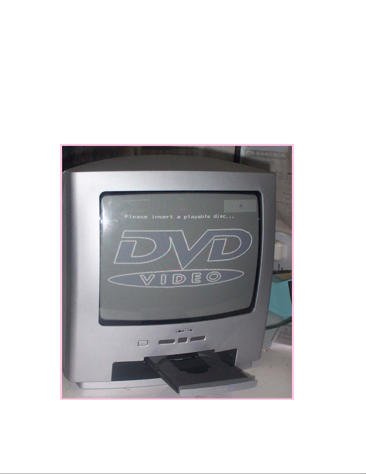
14” DVD COMBI TV
Page 2

CONTENTS
Page 3

1. TECHNICAL SPECIFICATIONS,
CONNECTIONS AND CHASSIS OVERVIEW
1.1. Technical Specifications
1.1.1 Reception
Tuning System : PLL
Color Systems : PAL SECAM NTSC
Sound Systems : B/G D/K L/L’
A/V Connections : SCART AND FRONT AV
Channel Selections : AIR : E2-E12, E21-E69
CABLE : S01-S41
IF Frequency : B/G, D/K, L : 38.9 MHZ
L’ : 33.4
I : 39.5MHZ
Aerial Input : 75 OHM
1.1.2 Miscellaneous
Audio Output (RMS) : 2 x 2.5 W
Mains Voltage : 220-240 V (± 10 %)
Mains Frequency : 50/60 Hz (± 5 %)
Ambient Temperature :
Maximum Humidity :
Power Consumption : 50 W
Standby Power Cosumption : 4 W
Page 4
1.2 Connections
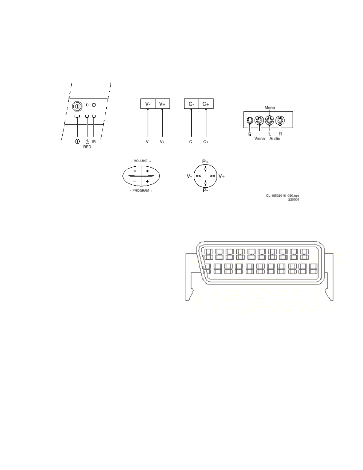
1.2.1 Front (or Side) Connections and Front (or Top) Control
1.2.2 EuroScart
Ht1
1. Audio Output 1. right cahnnel 0.5
VRMS/<1k0
2. Audio Input 1. right channel 0.5 VRMS
(connected to No.6)
3. Audio Output 2. left channel 0.5 VRMS
(connected to No.1)
4. GND (audio)
5. GND
6. Audio Input 2. left channel 0.5
VRMS/>10k0
7. RGB Input, blue (B)
8. Switch signal video (status)
9. GND
10. Reserved for clock signals (not connected)
11. RGB input, green (G)
12. Reserved for remote control
13. GND
14. GND switch signal RGB
15. RGB input, red (R)
16. Switch Signal RGB
17. GND (video)
18. GND19- video output 1 Vpp/75 ohm
19. Video Output
20. Video input 1 Vpp/75 ohm
21. Shield
20 18 16 14 12 10 8 6 4 2
21 19 17 15 13 11 9 7 5 3 1
Page 5

CHASSIS OVERVIEW
Page 6

2. SAFETY INSTRUCTIONS AND WARNINGS
SAFETY INSTRUCTIONS FOR SERVICE REPAIRS
1. Use only the original spare parts with the same specifications for replacement.
2. Only the original fuse value should be used.
3. Main leads and connecting leads should be checked for external damage before
connection. Insulation must be checked.
4. Parts contributing to the safety of the product must not be damaged nor obviously
unsuitable. This is valid especially for insulators and insulating parts.
5. Thermally loaded solder pads are to be sucked off and re-soldered.
6. Ensure that the ventilation slots are not obstructed.
7. Potentials as high as 25 KV are present when this receiver is operating. Operation
of the receiver outside the cabinet or with back cover removed involve a shock
hazard from the receiver.
8. Servicing should not be attempted by anyone who is not throughly familiar with
precautions necessary when working on high voltage equipment. Perfectly
discharge the high potential of the picture tube before handling it. The picture
tube is highly evacuated and if broken. Glass fragments will be violently expelled.
Always discharge the picture tube anode to the receiver chassis to keep of the
shock hazard before removing the anode cap.
9. Keep wire away from the high voltag or high temperature components.
10. When replacing a wattage resistor, keep the resistor 10mm away from the circuit
board.
11. Fast heating up (e.g. by bringing the Combi from a cold place into warm and
humid room) can result in moisture condensing on the pickup lens of the DVD
Module, thus influencing the playability for a certain time. Before checking the
performance, the DVD Loader should be stabilized for at least 4 hours.
12. Never try to repair DVD module when it is ON. The laser beam is highly
dangerous and it may cause permanent damages.
HANDLING THE MOS CHIP COMPONENTS
MOS circuit requires special attention with regard to static charges. Static charges may
occur with any highly insulated plastics and can be transferred to persons wearing clothes
and shoes made of synthetic materials. Protective circuits on the inputs and outputs of
MOS circuits give protection to a limited extend only due to time of reaction.
Please observe the following instructions to protect the components against ESD.
Page 7

1. Keep MOS components in conductive package until they are used. Most
components must never be stored in styropor materials or plastic magazines.
2. Personnel must not touch the MOS components to avoid electrostatic discharging.
3. Hold the component by the body touching the terminals.
4. Use only grounded instruments for testing and processing purposes.
5. Remove or connect MOS Ics when operating voltage is disconnected.
6. Personnel in charge must make sure that they are connected with the same
potential as the mass of the set by a wrsitband with resistance.
X-RAY RADIATION PRECAUTION
1. Excessive high voltage can produce potentially hazardous X-RAY radiation. To
avoid suxh hazard, the high voltage must not be above the specified limit. The
nominal value of the high voltage of this receiver is 25KV at zero beam current
(minimum brightness) under 220 V AC power source. The high voltage must not
under any circumstance, exceed 30KV. It is recommended the reading of the high
voltage to be recorded as a part of the service record. It is important to use an
accurate and reliable high voltage meter.
2. The primary source of X-RAY radiation in thi TV receiver is the picture tube. For
continued X-RAY radiation protection, the replacement tube must be exactly the
same type tube as specified in the part list.
Page 8

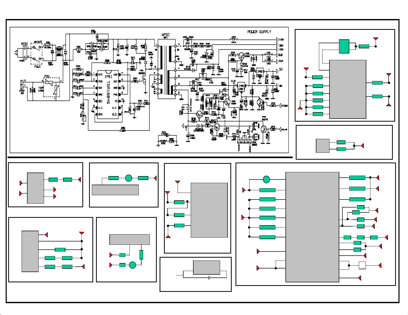
BLOCK DIAGRAM
A1 TUNER
10
A3 SCART
13
4 3 2
AV_STATUS
A2-1
A11
KEYBOARD
KEYB A7-1
IF1 A2-5
11
IF2 A2-4
SDA A4-1/A2-3
5
SCL A4-2/A2-2
4
AGC A2-1
1
SC_I A2-2
FBEXT A2-5
11
21
17
8 7 6
CLI A7-1 B A2-8
18
12
10
G A2-7
A4 EEPROM
SDA
A7-1/A2-1/A1-1
SCL
A1-2/A2-2/A7-2
AC IN
A2 VIDEO PEOCESSOR
AUDOUT A8-1
L/L’ A7-8
IF1 A2-5/A1-5
IF1 A2-5/A1-5
IF2 A1-4
AGC A1-1
AV_STATUS A3-1
SC_IN A3-2
CVBS A2-3
CVBS A3-3
SS01
9
CVBSEXT A3-4
B A3-8
G A3-7
5
15
19
16
20
14
SCART1
R A2-6
R A3-6
FBEXT A3-5
IC02
24C
08
5
6
1
2
6
7
8
11
14
13
20
25
26
27
28
STV2246/47/48
ICV1
55
SDA A7-1/A4-1/A1-3
52
SCL A7-2/A1-2/A4-2
51
HEATER A6-1/A7-7
49
HOUT A6-2
48
VERT A9-1
47
BCL A6-3
46
CVBSOUT A7-6
44
V_AMP A9-2
42
FB_OSD A7-10
37
R_OSD A7-3
36
G_OSD A7-4
35
B_OSD A7-5
34
A7 µ-CONTROLLER A8 AUDIO AMPLIFIER
IA01
TDA7057
CLI A3-1
MUTE_DVD
A8-10/A8-1/A10-1
L/L’ A2-8
TV/DVD A8-2
B_OSD A2-5
G_OSD A2-4
R_OSD A2-3
FB_OSD
A2-10/A7-5
SDA
A2-1/A4-1/A1-1
SCL
A2-2/A4-2/A1-2
8
11
12
13
15
16
17
18
19
25
ST92195/92185
IC01
56
KEYB A11-1
42
43
VOL A8-1
V_OSD A9-1
41
40
HEATER A2-7/A6-1
33
34
DVD SB
CVBSOUT
A2-6
FB_OSD
A7-5/A2-10
VOL A7-1
AUDOUT A2-1
MUTE_DVD
A8-10/A10-1/A7-1
L_DVD A10-2
A9 VERTICAL
VERT A2-1
18
ID41 TDA1771
2
43
3
IA03
2
MN405
1
3B
12
6
1
2
I060
7
LM358
V_AMP A2-2V_OSD A7-1
R_DVD
A10-3
2
3
T 46 DA168
IP01
WP02
14
11
110 V
16 V
5 VD
5 VA
12V
8 V
A6 HORIZONTAL A5 POWER SUPPLY
BCL A2-3
HOUT A2-2
HEATER
A10 AV INTERFACE CONN.
FBT
1
8
4
9
3
24 V
12 V
BS
_D
A8
SS08
1816151412
M
UT
UT
A8
E_
D
V
D
D
O
A7
-
1/
-4
A8
-
R_
L_
D
D
V
V
D
D
A8
A8
-3
-2
C
V
V
D
-5
Page 9
SUPPLY VOLTAGE DIAGRAM
A6
110V
16V
A9
1
2
TDA1
771
FBT
9
8
7
4
1
RD15 RD12
8
4
3
24V
12V
24V
RD45
RD44 RD56
RD28 RD40
8V
8V
12V
A3
19
8V TO SS05/4
A10
SS08
5V
8V
RV06
DV10
RV57
12
TV05
TV01
RV03
SS05
14
RV54
8V
A1
5V
5V
A4
5V
33V
LT01
RT03
RT01
9
7
3
1
TUNER
EEPROM
C011
A2
8V
LV07
SA02
1
2
12
17
25
26
27
28
16
11
56
55
54
46
45
43
41
40
39
34
33
31
VIDEO
PROC.
STV2246/47/48
+12V TO RA10
RA11
RS58
D005
D004
R052
D002
D001
53
45
8V
R002
R008
R057
R080
R081
R028 RA09
T001
5VA
5V
LV01
LV01
8V
5V
5V
5V
12VDVD
5VDVD
5V
5V
5VA
5VA
5V
LV01
LV03
DV23
DV22
DV21
8V
DV20
A8
IA03
MN4
053
A7
5V
5V
1 8
5VA
5VD
T003
R011
R010
R007
R032
R012
R013
2
3
12
13
14
19
20
21
25
26
ST92195/92185
Page 10
A1
TUNER
I2C BUS INTERCONNECTION DIAGRAM
A2
A4
A7
SDA
5
SDA
SDA
R013
SDA
SCL
4
SCL
RV33
RV34
SCL
R048
R049
SCL
51
52
6 5
VIDEO
PROC.
EEPROM
+5V
R012
SDA
SCL
20 19
u-CONTROLLER
Page 11

SERVICE MENU AND BASIC ADJUSTMENTS
SERVICE MODE IS ACTIVED BY PRESSING THE DIGIT “1923” IN THE
“FEATURES” MENU
a. SERVICE PARAMETERS
1.1 OPTION BYTES
OPTION 1: MODEL CONFIGURATION
b0 1: B/G Available 0: not available
b1 1: D/K Available 0: not available
b2 1: I Available 0: not available
b3 1: L Available 0: not available
b4-5 TTX National Character Set Group
00 : Set 1
01 : Set2
10 : Set3 (Turkish)
11 : Set3 (Turkish)
b6-7 Main Tuner
00 : Samsung
01 : Temic
10 : Philips UV1316
11 : Thomson/Orega
OPTION 2 : FEATURE CONFIGURATION
b0 1: Total Peak Lim. Avl. 0: Not Available
b1 1: QSS Application 0: Intercarrier Application
b2 1: Coring Available 0: Not Available
b3 1: Black Strecth Available 0: Not Available
b4 1: Blue Screen Enable 0: Disable
b5 1: OSD Contrast Control Enable 0: Disable
b6-b7 00: APR OFF
01: APR 50 IRE
10: APR 75 IRE
11: APR 100 IRE
Page 12

OPTION 3 : VIDEO/AUDIO FEATURE CONFIGURATION
b0 1: RGB Peak Lim. Available 0: not available/for2248E ver.
b1 1: SVHS mode available 0: not available
b2 1: DVD available 0: not available
b3 1: Tray Locked 0: Tray usage enabled
b4 1: One Xtal Appl. (4.43 Mhz) 0: 2 Xtal appl (for NTSC playback)
b5 1: AVC Auto Vol Correction 0: not available
b6 1: 2248E 0: 2248C
b7 1: Standby after power on 0: No Standby after power on
reserved bits must be set to 0
You will need following equipments to carry out the adjustment procedures;
a- PLL Pattern generator for Secam L'
b- PLL Pattern generator PAL BG
c- Patern generator for white pattern
d- Color Analyzer (CA100)
1.2 GEOMETRY ADJUSTMENT
a. V.SIZE 4/3 50H
b. V.SIZE 16/9 50H
c. V.SIZE 4/3 60H
d. V.SIZE 16/9 60H
e. V.POS
f. H.POS
• Enter service menu and select the GEOMETRY settings
• Standart geometrical adjustments carried out by VSIZE, VPOS AND HPOS settings.
VSIZE 16/9 50h setting have to be carried out until 3 cm distance between upper and
lower parts of the screen.
• Same adjustments for 60H for 16/9 and 4/3.
• Press “menu” button to leave service menu
• Same adjustments for 60Hz for 16/9 and 4/3.
• Press "Menu" button to leave service menu.
Page 13

1.3 G2 ADJUST
> : <
increase normal decrease
Enter the “G2” menu in the service mode
Turn the G2 potentiometer on FBT until you reach the : sign
< indicator means to decrease
> indicator means to increase
1.4 VIDEO
1 RED
2 GREEN
3 BLUE
4 RED COFF
5 GREEN COFF
• Apply Dark gray pattern (at 10 IRE)
• Contrast 70%, brightness middle, color saturation middle.
• By changing the RED C.OFF AND GREEN C.OFF Adjust to obtain the
necessary values for x and y.
• Apply white pattern (at 100 IRE)
• Set the contrast to 70%, brightness and color saturation to middle.
• Place the color analyzer.
• (R,G,B), it is possible to modify the peak white.
• Adjust to obtain the necessary values for x and y.
Remark: It may be necessary after low light alignment to check and to re-
align the high light and to repeat several times the procedure to obtain good
alignment for both low and high light.
Page 14

1.5 TUNER / IF
1. AGC
2. PIF COARSE
3. PIF FINE
4. PIF COARSE L’
5. PIF FINE L
PIF adjustment for BG/DK/L systems:
• 38.9 MHz PAL BG signal applied Tuner via tuner output (IF output).
• Leave the channel settings menu and enter service menu. Enter "TUNER IF"
menu in the service mode. Choose the "PIF COARSE" and “PIF FINE” item
and adjust the setting until the " : " indicator (displayed as " > : < ") turns in
red color by pressing < and > on remote control.
• Press "Menu" button to leave service menu.
PIF adjustment for L' system :
• 33.9 MHz SECAM L' signal applied Tuner via tuner output.
• Leave the channel settings menu and enter service menu. Enter "TUNER IF"
menu in the service mode. Choose the "PIF COARSE L’" and “PIF FINE L’ “
item and adjust the setting until the " : " indicator (displayed as " > : < ") turns
in red color by pressing < and > on remote control.
• Press "Menu" button to leave service menu.
1.6 HOTEL MODE
Installation and Child Lock Menus are omitted in Hotel Mode. You can not search
any channel when the Hotel Mode is activated.
Volume level can not be increased higher then certain level in Hotel Mode. The
volume limiting level is a pre-defined value in service menu.
• Switch the TV in AV mode by pressing "AV" button on remote control unit.
• Adjust the VAP2 potentiometer until 115Vdc measured on cathode pin of DP08
3. SYSTEM VOLTAGE ADJUSTMENT
(Minimum beam current condition)
diode.
Page 15

DVD MODULE
SAFETY AND HANDLING PRECAUTIONS
1. DO NOT use and store the Loader in dusty, high temperature or high humidty
environments.
2. To avoid damage to the Loader by electrostatic dischargers, measuring equipment
and operators should be grounded during handling. The user of this unit takes all
necessary precautions to avoid ESD (Electro-Static Discharge) failures during
handling and assembly of this unit into the end product.
3. Contamination of the PCB might influence the performance. Avoid fingerprints
and stains on the PCB and handle the Loader in a clean environment.
4. The mechanism of the Loader has been adjusted carefully during manufacturing.
High shocks on this unit may damage and should be avoided.
5. Fast heating (e.g. by bringing the Loader unit from a cold place into a warm and
humid room) can result in moisture condensing on the pickup lens, thus
influencing the playability for a certain time. Before checking the performance the
Loader unit should be stabilized for at least 4 hours.
6. DO NOT disamble the loader to avoid ESD failures and to prevent from
contamination.
AC SOURCE SUPPLY:
The Voltage Fluctuation : 110/220 V ± 10% tolerance
The Impulse Noise : 110/220 V ± 10% tolerance
Page 16

SPECIFICATION
Performance
Applicable Disc Format:
DVD-5, DVD-9, DVD-10, DVD-18, CVD, SVCD, DVCD, CD-R, CD-RW, VCD
CD-Audio
Rotational Speed
DVD: 2X(CLV) Approx. 1,100 rpm to 2,800 rpm.
CD: 4X(CLV) Approx. 792rpm to 2139 rpm
Data Transfer Rate
•Sustained Data Transfer Rate DVD: Approx. 2,760 KB/sec
VCD: Approx. Max 688 KB/sec
•Burst (ATAPI): 16.7 Mbytes/sec (PIO Mode 4)
Average Access Time
Random Access DVD : 250 ms Typical
CD : 250 ms Typical
Data Buffer Capacity 512 Kbytes
Error Rate
DVD Hard Error Rate: 10E-15 max.
Seek Error Rate : 10E-6 max.
CD Hard Error Rate : 10E-12 max. (Mode 1)
10E-9 max. (Mode 2)
Seek Error Rate : 10E-6 max.
Page 17
MECHANICAL AND ELECTRICAL
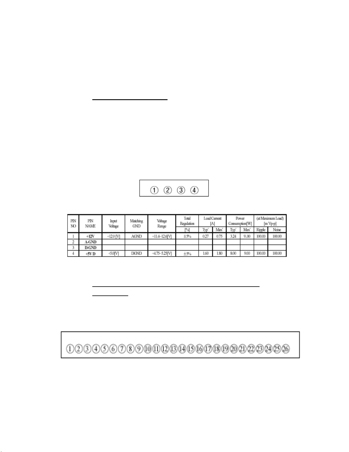
1. CONNECTORS
a. D.C Power Connector
A 4-pin shrouded, keyed male connector is used to be supplies with D.C. Power.
Maker : LG Cable
Specification : GIL-G-4P-S3T2(2.5mm pitch)
Matching Housing : GIL-G-4S-S3T2
b. Audio/Video Output And Digital Audio Interface
Connector
A 26-pin 1.0mm Pitch FFC/FPC connector is applied
Page 18
Maker: LG Cable
Specification: GF102-26S-TS
Matching FFC/FPC Type : 1.00mm pitch FFC Cable(Top Contact)
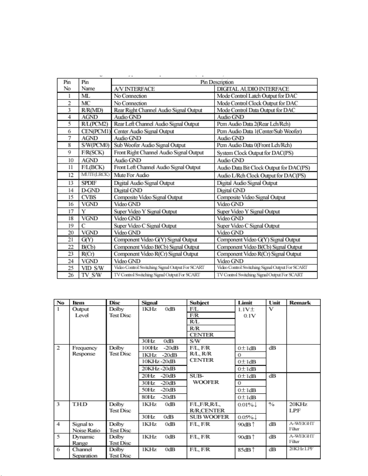
2.
AUDIO PERFORMANCE
Page 19
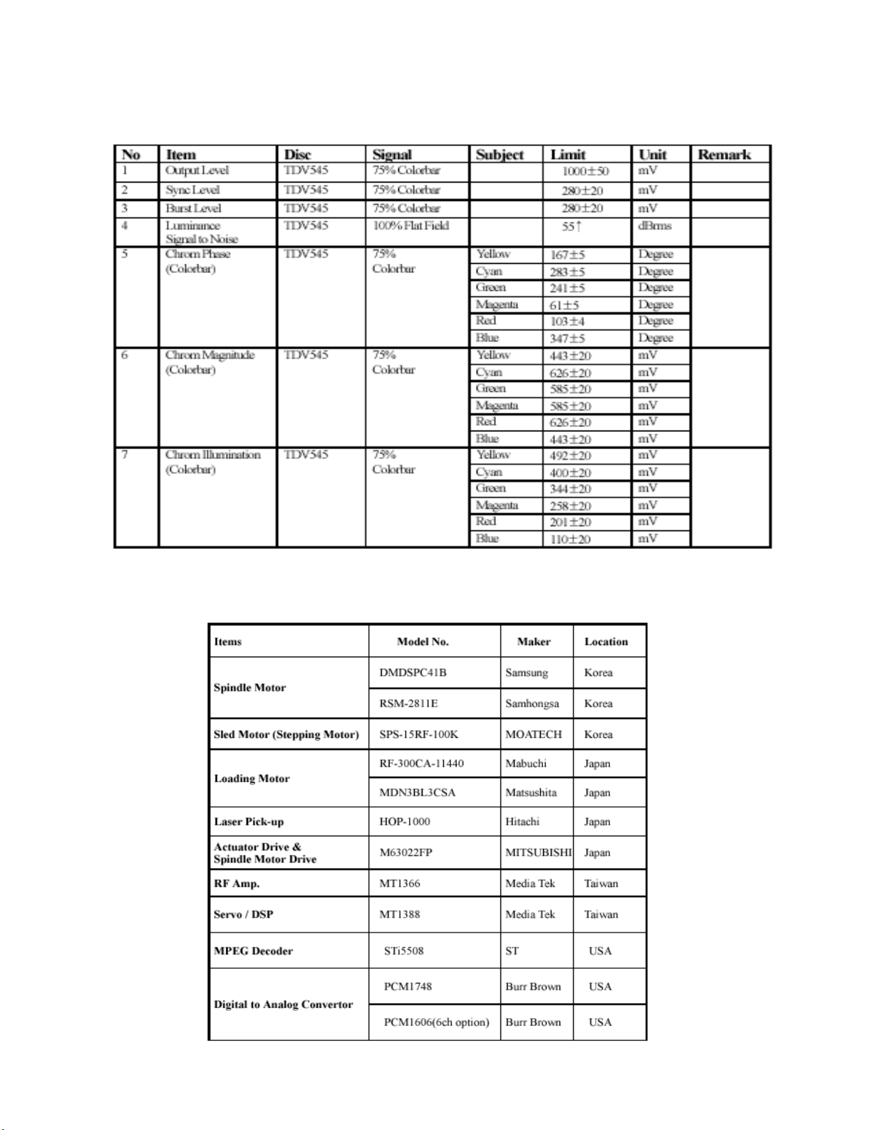
3. VIDEO PERFORMANCE
4. KEY COMPONENT LIST
Page 20

5. MECHANICAL DIMENSIONS
Page 21

BLOCK DIAGRAMS
Page 22

Page 23
D5
D1
D5
D4
D3
D2
D1
D2
D3
D4
Page 24

Page 25

Page 26

D1
D1
Page 27

D2
D1
D1
D2
Page 28

D2
D1
D1
D2
Page 29

Page 30

D2
D2D1
Page 31

Page 32

Page 33

DVD MODULE
DSL-760
STI5519
Page 34

R302 D1
R335 D1
R340 D1
R343 B1
R344 B1
R345 B1
R346 B1
R350 A1
R351 A1
R309 A1
R310 A1
R347 A1
R348 A1
R349 A1
C304 A1
EC307 A1
R301 D2
RA301 D2
RA303 D2
RA304 D2
RA305 D2
RA306 D2
RA307 C2
RA308 C2
RA309 C2
RA310 C2
RA311 C2
R337 C2
R303 B2
R304 B2
R305 B2
R336 B2
R308 A1
C313 A1
C314 A1
C315 A1
C316 A1
C317 A1
C318 A1
C319 A1
C320 A1
C321 A1
C322 A1
C330 A1
C331 A1
C332 A1
C333 A1
C334 A1
C335 A1
R320 A1
EC308 A1
EC305 A1
R341 D3
R342 D3
R325 D3
R326 D3
C305 D3
EC304 D3
R311 A3
R312 A3
C301 A3
EC301 A3
R422 A3
C302 A3
EC302 A3
EC306 A3
C323 A3
C324 A3
C325 A3
C326 A3
C327 A3
C328 A3
C329 A3
C337 A3
R324 D4
R322 D4
R333 D4
R332 D4
R331 D4
R330 D4
C312 D4
Q301 D4
Q302 D4
R327 D4
R321 D4
R319 C4
R315 C4
R316 C4
R317 C4
R318 C4
RA302 B4
C303 A4
EC303 A4
R421 A4
R328 D5
R339 D5
R329 D5
C309 D5
C310 D5
C311 D5
R334 C5
R423 A5
R313 A5
R314 A5
Page 35

1 2
3
4 5
D
D
C
C
B
B
C435 A1
L407 A2
C436 A2
R454 C2
R455 C2
R456 C2
R451 C2
R452 C2
R453 C2
EC417 B2
C434 A2
D401 D4
R440 D4
U402 D4
R419 D5
R417 D5
EC413 D5
R413 C4
C427 C5
EC408 C5
R411 C4
EC409 C5
C428 C5
L403 B5
L404 B5
L402 A5
A
A
DSL-760
PCM1748
1
234
Page 36

1 2
3
4 5
R501 D1
D
C
B
A
R502 D2
R503 D2
R504 D2
R505 D2
EC501 D2
Q501 D2
R509 D2
R510 D2
Q502 D2
EC502 D2
R507 C2
R508 C2
R511 C2
R513 C2
R514 C2
R515 C2
R516 C2
R518 C2
Q503 C2
EC503 C2
R519 B2
R520 B2
R521 B2
R522 B2
R524 B2
EC504 B2
Q504 B2
R526 B2
R528 B2
Q505 B2
EC505 B2
R525 A2
R527 A2
R530 A2
R531 A2
D
C
B
A
DSL-760
R532 A2
R533 A2
R534 A2
R536 A2
EC506 A2
Q506 A2
C501 D3
R506 D3
C505 D3
R512 D3
C502 D3
C506 D3
C509 C3
C510 C3
R517 C3
C513 B3
C514 B3
R523 B3
C517 B3
C518 B3
R529 B3
C521 A3
C522 A3
R535 A3
L501 C5
EC507 C4
C523 C4
1
2
34
VIDEO AMP
Page 37

DESCRIPTION OF INTEGRATED CIRCUITS
-TV PART-
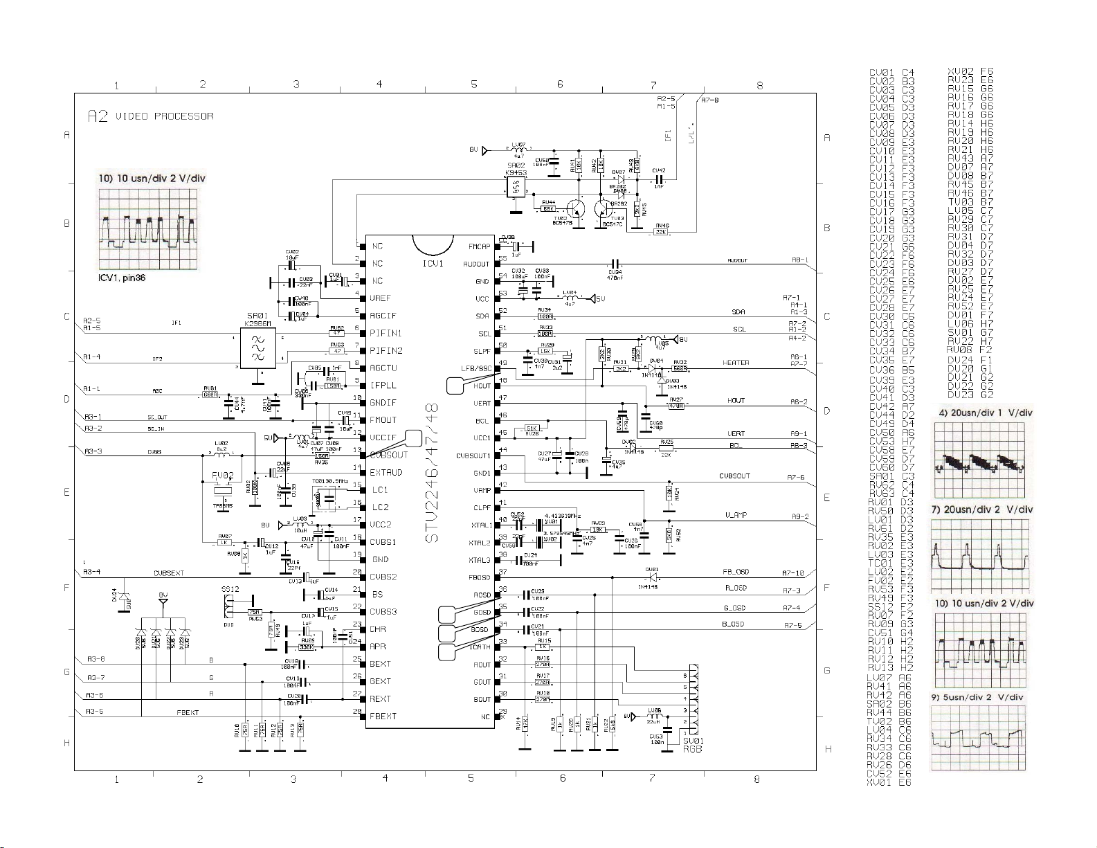
STV224X pos: ICV1
Multi Standard TV Processor
STV224X is a fully bus controlled IC for TV including PIF, SIF , Luminance , Chrominance and
deflection processing. It is a bus controlled PAL / SECAM / NTSC single chip TV Processor. For
details of STV224X features please refer to the STV224X datasheet. 110° , 4:3 or 16:9 CRT
applications. It integrates both vertical deflection and E-W correction circuit necessary for design
of 110° chassis it allows designing a PAL/NTSC(BGDKIMN) set with very few external
components and no manual adjustment.
Page 38

PIN CONFIGURATION
Page 39

Page 40

Page 41

MAIN FEATURES
- I²C bus control (read and write modes),
- PIF PLL demodulator, Bus controlled VCO alignment,
- IF positive and negative modulation,
- Digital AFC,
- Tuner delayed AGC output,
- White and Black spot cancellation,
- SIF with QSS or intercarrier structure,
- Built in sound bandpass,
- Multistandard PLL FM demodulator (4.5, 5.5, 6.0,6.5MHz),
- AM demodulator for France,
- FM sound carriers output for Stereo chassis,
- Audio switch for external audio input, Mono chassis,
- Digital volume control,
- Audio Mute,
- Video switch, 3 CVBS inputs, 1 CVBS output which can be used to drive teletext decoder,
- SVHS switch, Y input is combined with CVBS3 input,
- OSD RGB analog inputs, fast blanking detection on OSD fast blanking pin,contrast control
capability,oversize blanking capability on OSD fast blanking input,
- External analog RGB inputs with contrast and saturation control (external RGB matrixed in
YUV).
- Integrated chroma filters (trap, bandpass, cloche) with automatic alignment,
- Integrated luminance delay line,
- Adjustable peaking on the luminance signal with coring function,
- Black strech circuit,
- PAL/SECAM/NTSC color decoder with automatic identification of standards,
- Integrated chroma delay line,
- Full integrated SECAM decoder,
- Hue control, two selectable matrixes in NTSC mode,
- Automatic flesh control circuit with two selectable characteristics (normal and wide),
- ACC overload circuit,
- Chroma subcarrier output which could be used to drive comb filter circuit,
- Automatic RGB peak regulation (APR).
- Automatic digital cut-off current loop with warm-up detection circuit,
- White point and cut-off point adjustments,
- Beam current limiter control stage,
- High performance synchronization pulses separator,
- Horizontal synchronization with two phase locked loops,
- Integrated VCO, auto-calibration using the chroma crystal reference frequency,
- Automatic time constant selection for the first PLL, 3 selectable time contants,
- Video identification circuit (independant from PLL1),
- Noise detector circuit,
- Vertical countdown circuit,
- Automatic 50/60Hz selection circuit,
- Blanking and inserted cut-off pulses position adapted to standard (50 or 60Hz),
- Long blanking mode capability in 60Hz (same blanking as 50Hz standard),
- Possibility to insert cut-off pulses after a vertical oversize blanking signal,
- De-interlace capability,
- Horizontal starting circuit with soft-start capability,
- Horizontal and vertical position adjustments, vertical amplitude control voltage (combined with
chroma subcarrier output),
- 4/3, 16/9 selection voltage.
Page 42

Page 43

ST92195C/D pos: IC01
48-96 KB ROM HCMOS MCU WITH ON-SCREEN
DISPLAY AND TELETEXT DATA SLICER
General Features:
• Register File based 8/16 bit Core Architecture with RUN, WFI, SLOW and HALT
modes
• 0°C to +70°C Operating Temperature Range available
• Up to 24 MHz Operation @ 5V±10%
• Minimum instruction cycle time: 165nS at 24MHz.
• 48, 56, 64, 84 or 64K Bytes ROM
• 256 Bytes RAM of Register file (accumulators or index registers)
• 256 to 512 Bytes of on-chip static RAM
• 2 or 8 Kbytes of TDSRAM (Teletext and Display Storage RAM)
• 28 fully programmable I/O pins
• Serial Peripheral Interface
• Flexible Clock controller for OSD, Data Slicer and Core clocks running from
a single low frequency external crystal.
• Enhanced Display Controller with 26 rows of 40/80 characters
– 2 sets of 512 characters
– Serial and Parallel attributes
– 10x10 dot Matrix, definable by user
– 4/3 and 16/9 supported in 50/60HZ and 100/120 Hz mode
– Rounding, fringe, double width, double height, scrolling, cursor, full
Background color, half-intensity color, translucency and half-tone modes
• Teletext unit, including Data slicer, Acquisition Unit and up to 8K Bytes
RAM for Data Storage
• VPS and Wide Screen Signalling slicer
• Integrated Sync Extractor and Sync Controller
• 14-bit Voltage Synthesis for tuning reference voltage
• Up to 6 External Interrupts plus one non-maskable interrupt
• 8 x 8-bit programmable PWM outputs with 5V open-drain or push-pull
capability
• 16-bit Watchdog timer with 8-bit prescaler
• 1 or 2 16-bit standard timer(s) with 8-bit prescaler
• I²C Master/Slave (on some devices)
• 4-channel A/D converter; 5-bit guaranteed
• Rich instruction set and 14-Addressing modes
• Versatile development tools, including Assembler, Linker, C-Compiler, Archiver, Source
Level Debugger and hardware emulators with Real-Time Operating System available
from third parties
• Pin Compatible EPROM and OTP devices available.
Page 44

Microcontroller+OSD+(Teletext decoder)+VPS/PDC/WSS decoder are embedded in one
chip, where there are two types with the major difference;
ST92185 No-teletext
ST92195 With teletext
The ST92195 microcontroller is developed and manufactured by STMicroelectronics using a proprietary n-well HCMOS process. Its performance derives from the use of a flexible 256-register
pro-gramming model for ultra-fast context switching and real-time event response. The
intelligent on-chip peripherals offload the ST9 core from I/O and data management processing
tasks allowing critical application tasks to get the maximum use of core resources. The ST92195
MCU supports low power consumption and low voltage operation for power-efficient and low-cost
embedded systems.
The advanced ST9+ Core consists of the Central Processing Unit (CPU), the Register File and the
Interrupt controller. The general-purpose registers can be used as accumulators, index registers,
or address pointers. Adjacent register pairs make up 16-bit registers for addressing or 16-bit
processing. Although the ST9 has an 8-bit ALU, the chip handles 16-bit operations, including
arithmetic, loads/stores, and memory/register and memory/memory exchanges. Two basic
addressable spaces are available: the Memory space and the Register File, which includes the
control and status registers of the on-chip peripherals. power consumption of the device can be
reduced by more than 95% (Low power WFI).
Up to 28 I/O lines are dedicated to digital Input/Output. These lines are grouped into up to five
I/O Ports and can be configured on a bit basis under software control to provide timing, status
signals, timer and output, analogue inputs, external interrupts and serial or parallel I/O. A set of
on-chip peripherals form a complete system for TV set and VCR applications:
– Voltage Synthesis
– VPS/WSS Slicer
– Teletext Slicer
– Teletext Display RAM
– OSD
Page 45

BLOCK DIAGRAM
PIN DESCRIPTION
Page 46

Page 47

PIN ASSIGNMENT
Pin No. Pin Name I/O Function
1 INT7/P2.0 IR INT. IN
3 P0.7 DVDDATAOUT
4 P0.6 STOP
5 P0.5 N.C.
6 P0.4 N.C.
7 P0.3 N.C.
8 AIN4 AV.STATUS
9 P0.1 N.C.
10 P0.0 N.C.
11
12 P3.6 L/L'
13 P3.5 TV/DVD
14 P3.4 STDBY
28 JTCK N.C.
30 CVBSO N.C.
32 JTMS N.C.
42 P4.0/PWMO DVD_STD_BY
43 P4.1/PWM1 VOL
44 P4.2/PWM2 N.C.
45 P4.3/PWM3 DVD POWER +5V
46 P4.4/PWM4 DVD POWER +12V
47 P4.5/PWM5 N.C.
48 P4.6/PWM6 N.C.
49
53 P2.4/NMI N.C.
54 P2.3/INT6/VS01 LED CONTROL
55 P2.2/INT0/AIN2 DVDDATAIN
56 P2.1/INT5/AIN1 KEYBOARD INPUT
CSO/RESET0/P3.7
P4.7/PWM7/EXTRG/STOUT
MUTE_DVD
N.C.
Page 48

24C08 pos: IC02
Non-Volatile Memory
These I²C-compatible electrically erasable programmable memory (E²PROM) is organized as
1024 x 8 bit and operate with a power supply of 5 V. The memory behaves as a slave device in
the I²C protocol, with all memory operations synchronized by the serial clock. Read and Write
operations are initiated by a START
condition, generated by the bus master. The START condition is followed by a Device Select Code
and RW bit terminated by an acknowledge bit.
Page 49

TDA1771 pos: ID41
VERTICAL DEFLECTION CIRCUIT
DESCRIPTION
The TDA1771 is a monolithic integrated circuit in SIP10 package.
It is a full performance and very efficient vertical deflection circuit intended for direct drive of a
TV picture tube in Color and B & W television as well as in Monitor and Data displays.
• RAMP GENERATOR
• INDEPENDENT AMPLITUDE ADJUSTEMENT
• BUFFER STAGE
• POWER AMPLIFIER
• FLYBACK GENERATOR
• INTERNAL REFERENCE VOLTAGE
• THERMAL PROTECTION
Page 50

Page 51

Page 52

TDA 16846 pos: IP01
Controller for Switch Mode Power Supplies
Supporting Low Power Standby and Power
Factor Correction
Features
• Line Current Consumption with PFC
• Low Power Consumption
• Stable and Adjustable Standby Frequency
• Very Low Start-up Current
• Soft-Start for Quiet Start-up
• Free usable Fault Comparators
• Synchronization and Fixed Frequency Facility
• Over- and Undervoltage Lockout
• Switch Off at Mains Undervoltage
• Temporary high power circuit (only TDA 16847)
• Mains Voltage Dependent Fold Back Point Correction
• Continuous Frequency Reduction with Decreasing Load
• Adjustable and Voltage Dependent Ringing Suppression Time
Description
The TDA 16846 is optimized to control free running or fixed frequency flyback
converters with or without Power Factor Correction (Current Pump). To provide low
power consumption at light loads, this device reduces the switching frequency
continuously with load, towards an adjustable minimum (e. g. 20 kHz in standby mode).
Additionally, the start up current is very low. To avoid switching stresses of the power
devices, the power transistor is always switched on at minimum voltage. A special circuit
V
is implemented to avoid jitter. The device has several protection functions:
and undervoltage, mains undervoltage, current limiting and 2 free usable fault
comparators. Regulation can be done by using the internal error amplifier or an opto
coupler feedback (additional input). The output driver is ideally suited for driving a
power MOSFET, but it can also be used for a bipolar transistor. Fixed frequency and
synchronized operation are also possible. The TDA 16846 is suited for TV-, VCR- sets
and SAT receivers. It also can be good used in PC monitors. The TDA 16847 is identical
with TDA 16846 but has an additional power measurement output (pin 8) which can be
used for a Temporary High Power Circuit.
CC over-
Page 53

Pin Definitions and Functions
Pin Symbol Function
1 OTC Off Time Circuit
2 PCS Primary Current Simulation
3 RZI Regulation and Zero Crossing Input
4 SRC Soft-Start and Regulation Capacitor
5 OCI Opto Coupler Input
6 FC2 Fault Comparator 2
7 SYN Synchronization Input
8 N.C./PMO Not Connected (TDA16846)/PMO (TDA16847)
9 REF Reference Voltage and Current
10 FC1 Fault Comparator 1
11 PVC Primary Voltage Check
12 GND Ground
13 OUT Output
14 VCC Supply Voltage
Short Description of the Pin Functions
Pin Function
1
A parallel RC-circuit between this pin and ground determines the
ringing suppression time and the standby-frequency.
2
A capacitor between this pin and ground and a resistor between
this pin and the positive terminal of the primary elcap quantifies the
max. possible output power of the SMPS.
Page 54

3 This is the input of the error amplifier and the zero crossing input.
The output of a voltage divider between the control winding and
ground is connected to this input. If the pulses at pin 3 exceed a 5V
threshold, the control voltage at pin 4 is lowered.
4
This is the pin for the control voltage. A capacitor has to be
connected between this pin and ground. The value of this capacitor
determines the duration of the softstart and the speed of the
control.
5
If an opto coupler for the control is used, it’s output has to be
connected between this pin and ground. The voltage divider at pin3
has then to be changed, so that the pulses at pin3 are below 5 V.
6
Fault comparator 2: If a voltage > 1.2 V is applied to this pin, the
SMPS stops.
7
If fixed frequency mode is wanted, a parallel RC circuit has to be
connected between this pin and ground. The RC-value determines
the frequency. If synchronized mode is wanted, sync pulses have to
be fed into this pin.
8
Not connected (TDA16846). / This is the power measurement
output of the Temporary High Power Circuit. A capacitor and a RCcircuit has to be connected between this pin and ground
(TDA16847).
9
Output for reference voltage (5 V). With a resistor between this pin
and ground the fault comparator 2 (pin 6) is enabled.
10
Fault comparator 1: If a voltage > 1 V is applied to this pin, the
SMPS stops.
11
This is the input of the primary voltage check. The voltage at the
anode of the primary elcap has to be fed to this pin via a voltage
divider. If the voltage of this pin falls below 1 V, the SMPS is
switched off. A second function of this pin is the primary voltage
dependent fold back point correction (only active in free running
mode).
12
Common ground.
13
Output signal. This pin has to be connected across a serial resistor
with the gate of the power transistor.
14
Connection for supply voltage and startup capacitor. After startup
the supply voltage is produced by the control winding of the
transformer and rectified by an external diode.
Page 55

Block Diagram
Page 56

TDA7057AQ pos: IA01
2 x 5 W stereo BTL audio output amplifier with DC
volume control
FEATURES
• DC volume control
• Few external components
• Mute mode
• Thermal protection
• Short-circuit proof
• No switch-on and switch-off clicks
• Good overall stability
• Low power consumption
• Low HF radiation
• ESD protected on all pins.
Page 57

Page 58

74HC4053B pos:IA03
Analog Multiplexer/Demultiplexer
Page 59

LM317 pos: IP02
1.2V TO 37V Voltage Regulator
LM358 pos: I060
Dual Operational Amplifier
Page 60

Page 61

LM7805 pos: IP03
3-Terminal 1A Positive Voltage Regulator
Page 62

DESCRIPTION OF INTEGRATED CIRCUITS
-DVD PART-
STi5519 pos: U301
DVD HOST PROCESSOR WITH ENHANCED AUDIO FEATURES
Page 63

Page 64

PINNING
Page 65

Page 66

Page 67

Page 68

Page 69

Page 70

M29W800AT pos: U302
8Mbit Low Voltage Single Supply Flash Memory
Page 71

M24C02 pos: U306
1 Kbit I²C Bus EEPROM
Page 72

Page 73

HY57V651620B (64M) pos: U303
4Banks X 1M X 16Bit Synchronous DRAM
Page 74

PCM1748 pos: U405
24-Bit, 96kHz Sampling Enhanced Multilevel,DeltaSigma,Audio DIGITAL-TO-ANALOG CONVERTER
Page 75

DESCRIPTION
The PCM1748 is a CMOS, monolithic, integrated circuit, which includes stereo Digitalto-Analog Converters (DACs) and support circuitry in a small SSOP-16 package. The
data converters utilize Texas Instrument’s enhanced multilevel delta-sigma architecture
that employs fourth-order noise shaping and 8-level amplitude quantization to achieve
excellent dynamic performance and im-proved tolerance to clock jitter. The PCM1748
accepts industry standard audio data formats with 16- to 24-bit data, providing easy
interfacing to audio DSP and decoder chips. Sampling rates up to 100kHz are supported.
A full set of user-programmable functions are accessible through a 3-wire serial control
port that supports register write functions.
FEATURES
24-BIT RESOLUTION
ANALOG PERFORMANCE (V CC =+5V):
Dynamic Range: 106dB typ (PCM1748KE)
100dB typ (PCM1748E)
SNR: 106dB typ (PCM1748KE)
100dB typ (PCM1748E)
THD+N: 0.002%typ (PCM1748KE)
0.003%typ (PCM1748E)
Full-Scale Output: 3.1Vp-p typ
8x OVERSAMPLING DIGITAL FILTER:
Stopband Attenuation: –55dB
Passband Ripple: ±0.03dB
SAMPLING FREQUENCY:5kHz to 100kHz
Page 76

SYSTEM CLOCK:256,384,512,768f S with
Auto Detect
ACCEPTS 16-,18-,20-,AND 24-BIT AUDIO DATAzx
DATA FORMATS:Standard,I 2 S,and Left-Justified
USER-PROGRAMMABLE MODE CONTROLS:
Digital Attenuation:0dB to –63dB,0.5dB/Step
Digital De-Emphasis
Digital Filter Roll-Off:Sharp or Slow
Soft Mute
Zero Flags for Each Output
DUAL-SUPPLY OPERATION: +5V Analog,+3.3V Digital
5V TOLERANT DIGITAL INPUTS
SMALL SSOP-16 PACKAGE
SAME PACKAGE SIZE AS SOP-8
APPLICATIONS
A/V RECEIVERS
DVD MOVIE PLAYERS
DVD ADD-ON CARDS FOR HIGH-END PCs
HDTV RECEIVERS
CAR AUDIO SYSTEMS
OTHER MULTICHANNEL AUDIO SYSTEMS
MM74HCU04 pos: U307
Hex Inverter
General Description
The MM74HCU04 inverters utilize advanced silicon-gate CMOS technology to
achieve operating speeds similar to LS-TTL gates with the low power
consumption of standard CMOS integrated circuits. The MM74HCU04 is an
unbuffered inverter. It has high noise immunity and the ability to drive 15 LS-TTL
loads. The 74HCU logic family is functionally as well as pin-out compatible with
the standard 74LS logic family. All inputs are protected from damage due to
static discharge by inter-nal diode clamps to V CC and ground.
Features
■ Typical propagation delay: 7 ns
■ Fanout of 15 LS-TTL loads
■ Quiescent power consumption: 10 mA maximum at roomtemperature
■ Low input current: 1 mA maximum
Page 77

PCM1606 pos: U406
24-BIT, 192-kHz SAMPLING, 6-CHANNEL, ENHANCED
MULTILEVEL, DELTA-SIGMA DIGITAL-TO-ANALOG
CONVERTER
FEATURES
24-Bit Resolution
Analog Performance:
1. Dynamic Range: 103 dB, Typical
2. SNR: 103 dB, Typical
3. THD+N: 0.004%, Typical
4. Full-Scale Output: 3.1 Vp-p, Typical
8.... Oversampling Interpolation Filter:
1. Stopband Attenuation: –55 dB
2. Passband Ripple: ±0.03 dB
Sampling Frequency:
1. 5 kHz to 200 kHz (Channels 1 and 2)
2. 5 kHz to 100 kHz (Channels 3, 4, 5, and 6)
Accepts 16- and 24-Bit Audio Data
Data Formats: Standard, I²S, and Left-Justified, TDM
System Clock: 128 f
Digital De-Emphasis for 32 kHz, 44.1 kHz, 48 kHz
Power Supply: 5-V Single Supply
, 192 fS, 256 fS, 384 fS, 512 fS, or 768 fS
S
Page 78

20-Lead SSOP Package
DESCRIPTION
The PCM1606 is a CMOS monolithic integrated circuit that features six 24-bit
audio digital-to-analog converters and support circuitry in a small 20-lead SSOP
package. The digital-to-analog converters utilize Texas Instruments’ enhanced
multilevel, delta-sigma architecture, which employs 2 nd -order noise shaping
and 8-level amplitude quantization to achieve excellent signal-to-noise
performance and a high tolerance to clock jitter. The PCM1606 accepts industrystandard audio data formats with 16- to 24-bit audio data. Sampling rates up to
200 kHz are supported.
PIN ASSIGNMENT
Page 79

 Loading...