

Philips TDA9808-V3 Datasheet

DATA SH EET
Product specification
Supersedes data of 1999 Jan 18
File under Integrated Circuits, IC02
1999 Jun 04
INTEGRATED CIRCUITS
TDA9808
Single standard VIF-PLL with
QSS-IF and FM-PLL demodulator

1999 Jun 04 2
Philips Semiconductors Product specification
Single standard VIF-PLL with QSS-IF and
FM-PLL demodulator
TDA9808
FEATURES
• 5 V supply voltage (9 V supply voltage for TDA9808
(DIP20) only)
• Applicable for IFs (Intermediate Frequencies) of
38.9 MHz, 45.75 MHz and 58.75 MHz
• Gain controlled wide band Video IF (VIF)-amplifier
(AC-coupled)
• True synchronous demodulation with active carrier
regeneration (very linear demodulation, good
intermodulation figures, reduced harmonics, excellent
pulse response)
• Robustness for over-modulation better than 105% due
to Phase Locked Loop (PLL)-bandwidth control at
negative modulated standards
• VIF Automatic Gain Control (AGC) detector for gain
control, operating as peak sync detector
• Tuner AGC with adjustable TakeOver Point (TOP)
• Automatic Frequency Control (AFC) detector without
extra reference circuit
• AC-coupled limiter amplifier for sound intercarrier signal
• Alignment-free FM-PLL demodulator with high linearity
• Sound IF (SIF) input for single reference Quasi Split
Sound (QSS) mode (PLL controlled); SIF AGC detector
for gain controlled SIF amplifier; single reference QSS
mixer for high performance
• Electrostatic Discharge (ESD) protection for all pins.
GENERAL DESCRIPTION
The TDA9808 is an integrated circuit for single standard
(negative modulated) vision IF signal processing and FM
demodulation, with single reference QSS-IF in TV and
VTR sets.
ORDERING INFORMATION
TYPE NUMBER
PACKAGE
NAME DESCRIPTION VERSION
TDA9808 DIP20
plastic dual in-line package; 20 leads (300 mil)
SOT146-1
TDA9808T SO20
plastic small outline package; 20 leads; body width 7.5 mm
SOT163-1

1999 Jun 04 3
Philips Semiconductors Product specification
Single standard VIF-PLL with QSS-IF and
FM-PLL demodulator
TDA9808
QUICK REFERENCE DATA
SYMBOL PARAMETER CONDITIONS MIN. TYP. MAX. UNIT
V
P
supply voltage VP= 9 V for TDA9808 (DIP20)
only
4.5 5 9.9 V
I
P
supply current 71 83 95 mA
V
i(VIF)(rms)
VIF input signal voltage sensitivity
(RMS value)
−1 dB video at output − 60 100 µV
V
o(video)(p-p)
video output signal voltage
(peak-to-peak value)
1.2 1.35 1.5 V
B
−3
−3 dB video bandwidth on pin 9 CL< 30 pF; RL> 1.5 kΩ; AC load 7 8 − MHz
S/N
W(video)
weighted signal-to-noise ratio for
video
56 60 − dB
α
IM(0.92)
intermodulation attenuation at ‘blue’ f = 0.92 MHz 58 64 − dB
α
IM(2.76)
intermodulation attenuation at ‘blue’ f = 2.76 MHz 58 64 − dB
α
H(sup)
suppression of harmonics in video
signal
35 40 − dB
V
i(SIF)(rms)
sound IF input signal voltage
sensitivity (RMS value)
−3 dB at intercarrier output − 50 100 µV
V
o(rms)
audio output signal voltage for FM
(RMS value)
M, N standard;
25 kHz modulation
0.4 0.5 0.6 V
THD total harmonic distortion 25 kHz modulation − 0.15 1.0 %
S/N
W(audio)
weighted signal-to-noise ratio 25 kHz modulation; τ =75µs5560−dB
1999 Jun 04 4
Philips Semiconductors Product specification
Single standard VIF-PLL with QSS-IF and
FM-PLL demodulator
TDA9808
This text is here in white to force landscape pages to be rotated correctly when browsing through the pdf in the Acrobat reader.This text is here in
_white to force landscape pages to be rotated correctly when browsing through the pdf in the Acrobat reader.This text is here inThis text is here in
white to force landscape pages to be rotated correctly when browsing through the pdf in the Acrobat reader. white to force landscape pages to be ...
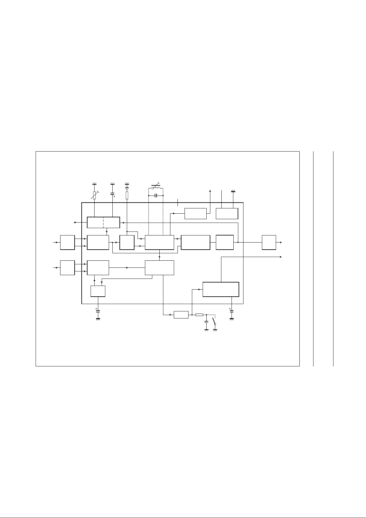
BLOCK DIAGRAM
handbook, full pagewidth
MHA736
VCO
TWD
SINGLE
REFERENCE
QSS MIXER
FPLL
VIF
AMPLIFIER
TUNER
AGC
VIF
AGC
VIF
SAW
SOUND
TRAP
VIDEO
DEMODULATOR
AND AMPLIFIER
AFC
DETECTOR
VOLTAGE
REFERENCE
GNDV
P
AFC
n.c.
2 x f
pc
T
PLL
C
VAGC
TADJ
TAGC
NOISE
CLIPPING
1
12
2
SIF
AMPLIFIER
SIF
SAW
SIF
AGC
C
SAGC
19
20
5
C
DEC
mute
switch
4.5 MHz
V
i FM
711
V
o QSS
10
9
6
13 18815144173 16
V
o(vid)
V
o AF
1.35 V (p-p)
FM-PLL
DEMODULATOR
TDA9808
Fig.1 Block diagram.
1999 Jun 04 5
Philips Semiconductors Product specification
Single standard VIF-PLL with QSS-IF and
FM-PLL demodulator
TDA9808
PINNING
SYMBOL PIN DESCRIPTION
V
i VIF1
1 VIF differential input signal voltage 1
V
i VIF2
2 VIF differential input signal voltage 2
TADJ 3 tuner AGC takeover point adjust
T
PLL
4 PLL loop filter
C
SAGC
5 SIF AGC capacitor
V
oAF
6 audio output
C
DEC
7 decoupling capacitor
n.c. 8 not connected
V
o(vid)
9 composite video output voltage
V
o QSS
10 single reference QSS output voltage
V
iFM
11 sound intercarrier input voltage
TAGC 12 tuner AGC output
AFC 13 AFC output
VCO1 14 VCO1 resonance circuit
VCO2 15 VCO2 resonance circuit
GND 16 ground
C
VAGC
17 VIF AGC capacitor
V
P
18 supply voltage
V
i SIF1
19 SIF differential input signal voltage 1
V
i SIF2
20 SIF differential input signal voltage 2
SYMBOL PIN DESCRIPTION
Fig.2 Pin configuration DIP20.
handbook, halfpage
MHA734
1
2
3
4
5
6
7
8
9
10
20
19
18
17
16
15
14
13
12
11
TDA9808
V
i VIF1
V
i VIF2
T
PLL
C
SAGC
V
o AF
V
o(vid)
V
o QSS
C
DEC
n.c.
TADJ
V
i SIF2
V
i SIF1
V
i FM
V
P
C
VAGC
GND
VCO2
VCO1
AFC
TAGC
Fig.3 Pin configuration SO20.
handbook, halfpage
MHA735
1
2
3
4
5
6
7
8
9
10
20
19
18
17
16
15
14
13
12
11
TDA9808T
V
i VIF1
V
i VIF2
T
PLL
C
SAGC
V
o AF
V
o(vid)
V
o QSS
C
DEC
n.c.
TADJ
V
i SIF2
V
i SIF1
V
i FM
V
P
C
VAGC
GND
VCO2
VCO1
AFC
TAGC

1999 Jun 04 6
Philips Semiconductors Product specification
Single standard VIF-PLL with QSS-IF and
FM-PLL demodulator
TDA9808
FUNCTIONAL DESCRIPTION
The integrated circuit comprises the functional blocks as
shown in Fig.1:
1. Vision IF amplifier and VIF AGC detector
2. Tuner AGC
3. Frequency Phase Locked Loop (FPLL) detector
4. Voltage Controlled Oscillator (VCO), Travelling Wave
Divider (TWD) and AFC
5. Video demodulator and amplifier
6. SIF amplifier and SIF AGC
7. Single reference QSS mixer
8. FM-PLL demodulator
9. Audio Frequency (AF) signal processing
10. Internal voltage stabilizer.
Vision IF amplifier and VIF AGC detector
The vision IF amplifier consists of three AC-coupled
differential amplifier stages. Each differential stage
comprises a feedback network controlled by emitter
degeneration.
The AGC detector generates the required VIF gain control
voltage for constant video output by charging/discharging
the AGC capacitor. Therefore, for negative video
modulation the synchronisation level of the video signal is
detected.
Tuner AGC
The AGC capacitor voltage is converted to an internal IF
control signal, and is fed to the tuner AGC to generate the
tuner AGC output current at pin TAGC (open-collector
output). The tuner AGC takeover point can be adjusted at
pin TADJ. This allows to match the tuner to the SAW filter
in order to achieve the optimum IF input level.
Frequency Phase Locked Loop (FPLL) detector
The VIF-amplifier output signal is fed into a frequency
detector and into a phase detector via a limiting amplifier.
During acquisition the frequency detector produces a DC
current proportional to the frequency difference between
the input and the VCO signal. After frequency lock-in the
phase detector produces a DC current proportional to the
phase difference between the VCO and the input signal.
The DC current of either the frequency detector or the
phase detector is converted to a DC voltage via the loop
filter, which controls the VCO frequency.
VCO, Travelling Wave Divider (TWD) and AFC
The VCO operates with a resonance circuit (with L and C
in parallel) at double the Picture Carrier (PC) frequency.
The VCO is controlled by two integrated variable
capacitors. The control voltage required to tune the VCO
from its free-running frequency to double the PC frequency
is generated by the frequency-phase detector of the FPLL
and fed via the loop filter to the first variable capacitor. This
control voltage is amplified and additionally converted into
a current which represents the AFC output signal. At the
centre frequency the AFC output current is equal to zero.
The oscillator signal is divided-by-two with a TWD which
generates two differential output signals with a 90 degree
phase difference independent of the frequency.
Video demodulator and amplifier
The video demodulator is realized by a multiplier which is
designed for low distortion and large bandwidth. The vision
IF input signal is multiplied with the ‘in phase’ signal of the
travelling wave divider output.
The demodulator output signal is fed to the video amplifier
via an integrated low-pass filter for attenuation of the
carrier harmonics. The video amplifier is realized by an
operational amplifier with internal feedback and high
bandwidth. A low-pass filter is integrated to achieve an
attenuation of the carrier harmonics. The video output
signal at pin V
o(vid)
is 1.35 V (p-p) for nominal vision IF
modulation. Noise clipping is provided.
SIF amplifier and SIF AGC
The sound IF amplifier consists of two AC-coupled
differential amplifier stages. Each differential stage
comprises a controlled feedback network provided by
emitter degeneration.
The SIF AGC detector is related to the SIF input signal
(average level of FM carrier) and controls the SIF amplifier
to provide a constant SIF signal to the single reference
QSS mixer.

1999 Jun 04 7
Philips Semiconductors Product specification
Single standard VIF-PLL with QSS-IF and
FM-PLL demodulator
TDA9808
Single reference QSS mixer
The single reference QSS mixer is realized by a multiplier.
The SIF amplifier output signal is fed to the single
reference QSS mixer and converted to intercarrier
frequency by the regenerated picture carrier (VCO).
The mixer output signal is fed via a high-pass filter for
attenuation of the video signal components to the output
pin 10. With this system a high performance hi-fi stereo
sound processing can be achieved.
FM-PLL demodulator
The FM-PLL demodulator consists of a limiter and an
FM-PLL. The limiter provides the amplification and
limitation of the FM sound intercarrier signal. The result is
high sensitivity and AM suppression. The amplifier
consists of 7 stages which are internally AC-coupled in
order to minimize the DC offset.
Furthermore the AF output signal can be muted by
connecting a resistor between the limiter input pin 11 and
ground.
The FM-PLL consists of an integrated relaxation oscillator,
an integrated loop filter and a phase detector.
The oscillator is locked to the FM intercarrier signal, output
from the limiter. As a result of locking, the oscillator
frequency tracks with the modulation of the input signal
and the oscillator control voltage is superimposed by the
AF voltage. The FM-PLL operates as an FM demodulator.
AF signal processing
The AF amplifier consists of two parts:
1. The AF pre-amplifier for FM sound is an operational
amplifier with internal feedback, high gain and high
common mode rejection. The AF voltage from the
PLL demodulator, by principle a small output signal, is
amplified by approximately 33 dB. The low-pass
characteristic of the amplifier reduces the harmonics of
the intercarrier signal at the sound output terminal
pin 10. An additional DC control circuit is implemented
to keep the DC level constant, independent of process
spread.
2. The AF output amplifier (10 dB) provides the required
output level by a rail-to-rail output stage. This amplifier
makes use of an input selector for switching to FM or
mute state, controlled by the mute switching voltage.
Internal voltage stabilizer
The bandgap circuit internally generates a voltage of
approximately 1.25 V, independent of supply voltage and
temperature. A voltage regulator circuit, connected to this
voltage, produces a constant voltage of 3.6 V which is
used as an internal reference voltage.

1999 Jun 04 8
Philips Semiconductors Product specification
Single standard VIF-PLL with QSS-IF and
FM-PLL demodulator
TDA9808
LIMITING VALUES
In accordance with the Absolute Maximum Rating System (IEC 134).
Notes
1. I
P
= 95 mA; T
amb
=70°C.
2. Machine model class B (L = 2.5 µH).
THERMAL CHARACTERISTICS
SYMBOL PARAMETER CONDITIONS MIN. MAX. UNIT
V
P
supply voltage note 1
T
j(max)
= 125 °C;
TDA9808 (DIP20)
− 9.9 V
T
j(max)
= 115 °C;
TDA9808T (SO20)
− 5.5 V
V
i
voltage at pins 1, 2, 5, 13, 17, 19 and 20 0 V
P
V
t
s(max)
maximum short-circuit time to ground or V
P
− 10 s
V
12
tuner AGC output voltage 0 13.2 V
T
stg
storage temperature −25 +150 °C
T
amb
operating ambient temperature −20 +70 °C
V
es
electrostatic handling voltage note 2 −300 +300 V
SYMBOL PARAMETER CONDITIONS VALUE UNIT
R
th(j-a)
thermal resistance from junction to ambient in free air
TDA9808 (DIP20) 62 K/W
TDA9808T (SO20) 85 K/W
1999 Jun 04 9
Philips Semiconductors Product specification
Single standard VIF-PLL with QSS-IF and
FM-PLL demodulator
TDA9808
CHARACTERISTICS (9 V SUPPLY, TDA9808; DIP20 only)
VP=9V; T
amb
=25°C; see Table 1 for input frequencies and carrier ratios; input level V
i(VIF)(rms)
=10mV
(pins 1 and 2) (sync-level); V
i(SIF)(rms)
= 4.5 mV (pins 19 and 20) (sound carrier); IF input from 50 Ω via broadband
transformer 1 : 1; video modulation DSB; residual carrier: 10%; video signal in accordance with
“NTC-7 Composite”
;
measurements taken in Fig.13; unless otherwise specified.
SYMBOL PARAMETER CONDITIONS MIN. TYP. MAX. UNIT
Supply (pin 18)
V
P
supply voltage note 1 4.5 5.0 9.9 V
I
P
supply current 72 85 98 mA
True synchronous video demodulator; note 2
V
i(VIF)(rms)
VIF input signal voltage
sensitivity (RMS value)
PLL still locked;
maximum IF gain; note 3
− 60 90 µV
Composite video amplifier (pin 9; sound carrier off)
V
o(video)(p-p)
video output signal voltage
(peak-to-peak value)
see Fig.8 1.27 1.45 1.63 V
S/N
W(video)
weighted signal-to-noise ratio see Fig.6 and note 4 56 60 − dB
PSRR power supply ripple rejection
at pin 9
see Fig.11 25 30 − dB
Tuner AGC (pin 12)
∆G
IF
IF slip by automatic gain
control
tuner gain current from
20 to 80%
− 68 dB
AFC circuit (pin 13); see Fig.10 and note 5
S control steepness ∆I13/∆f note 6
f
pc
= 38.9 MHz 0.35 0.55 0.75 µA/kHz
f
pc
= 45.75 MHz 0.35 0.55 0.75 µA/kHz
f
pc
= 58.75 MHz 0.35 0.55 0.75 µA/kHz
∆f
IF
/∆T frequency variation by
temperature
I
AFC
= 0; note 7 −−±20 × 10−6K
−1
FM-PLL sound demodulator and AF output (pin 6); note 8
V
o(AF)(6)(rms)
AF output signal voltage
(RMS value)
±25 kHz
(50% FM deviation);
see Fig.13
375 500 625 mV
S/N
W(audio)
weighted signal-to-noise ratio
“CCIR 468-4”
;
see Fig.13
55 60 − dB
α
6
mute attenuation 70 75 − dB
∆V
5
DC jump voltage of AF output
terminal
FM-PLL in lock mode −±50 ±175 mV

1999 Jun 04 10
Philips Semiconductors Product specification
Single standard VIF-PLL with QSS-IF and
FM-PLL demodulator
TDA9808
Notes to the characteristics
1. Values of video and sound parameters are decreased at VP= 4.5 V.
2. Loop bandwidth BL = 70 kHz (natural frequency fn= 12 kHz; damping factor d ≈ 3; calculated with sync level within
gain control range). Resonance circuit of VCO: Q0> 50; C
ext
: see Table 3; C
int
≈ 8.5 pF (loop voltage approximately
2.7 V).
3. V
i(VIF)
signal for nominal video signal.
4. S/N is the ratio of black to white amplitude to the black level noise voltage (RMS value, pin 9). B = 5 MHz weighted
in accordance with
“CCIR 567”
at a source impedance of 50 Ω.
5. To match the AFC output signal to different tuning systems a current source output is provided (Fig.10).
6. Depending on the ratio ∆C/C0 of the LC resonant circuit of VCO (Q0> 50; see note 2; C0=C
int+Cext
).
7. Temperature coefficient of external LC-circuit is equal to zero.
8. Input level for second IF from an external generator with 50 Ω source impedance. AC-coupled with 10 nF capacitor,
f
mod
= 1 kHz, 25 kHz (50% FM deviation) of audio reference. A VIF/SIF input signal is not permitted. Pin 17 has to be
connected to positive supply voltage. S/N and THD measurements are taken at 50 µs (75 µs at M standard)
de-emphasis.
1999 Jun 04 11
Philips Semiconductors Product specification
Single standard VIF-PLL with QSS-IF and
FM-PLL demodulator
TDA9808
CHARACTERISTICS (5 V SUPPLY)
V
P
=5V; T
amb
=25°C; see Table 1 for input frequencies and carrier ratios; input level V
i(VIF)(rms)
= 10 mV (pins 1 and 2)
(sync-level); V
i(SIF)(rms)
= 4.5 mV (pins 19 and 20) (sound carrier); IF input from 50 Ω via broadband transformer 1 : 1;
video modulation DSB; residual carrier: 10%; video signal in accordance with
“NTC-7 Composite”
; measurements taken
in Fig.13; unless otherwise specified.
SYMBOL PARAMETER CONDITIONS MIN. TYP. MAX. UNIT
Supply (pin 18)
V
P
supply voltage note 1 4.5 5 5.5 V
I
P
supply current 71 83 95 mA
Vision IF amplifier (pins 1 and 2)
V
i(rms)
allowable overload input
voltage (RMS value)
note 2 −−440 mV
V
I(max)(rms)
maximum input signal voltage
(RMS value)
+1 dB video at output;
see Fig.4
−−140 mV
V
i(VIF)(rms)
VIF input signal voltage
sensitivity (RMS value)
−1 dB video at output;
see Fig.4
− 60 100 µV
∆V
o(int)
internal IF amplitude
difference between picture
and sound carrier
within AGC range;
M standard;
∆f = 4.5 MHz
− 0.7 1 dB
G
IFcr
IF gain control range see Fig.4 65 70 − dB
R
i(diff)
differential input resistance note 3 1.7 2.2 2.7 kΩ
C
i(diff)
differential input capacitance note 3 1.2 1.7 2.5 pF
V
I(1,2)
DC input voltage note 3 − 3.4 − V
True synchronous video demodulator; note 4
f
VCO(max)
maximum oscillator frequency
for carrier regeneration
f=2f
pc
125 130 − MHz
∆f
osc
/∆T oscillator drift as a function of
temperature
oscillator is
free-running; I
AFC
=0;
note 5
−−±20 × 10
−6
K
−1
∆f
osc
/∆V
P
oscillator shift as a function of
supply voltage
oscillator is
free-running; note 5
−−±1500 × 10−6V
−1
V
VCO(rms)
oscillator voltage swing at
pins 14 and 15 (RMS value)
50 80 110 mV
f
cr(pc)
picture carrier capture range ±1.4 ±1.8 − MHz
t
acq
acquisition time BL = 70 kHz; note 6 −−30 ms
V
i(IF)(rms)
IF input signal voltage
sensitivity for PLL to be locked
(RMS value; pins 1 and 2)
maximum IF gain;
note 7
− 60 90 µV
 Loading...