

Philips tda9803 DATASHEETS

INTEGRATED CIRCUITS
DATA SH EET
TDA9803
Multistandard VIF-PLL
demodulator
Preliminary specification
File under Integrated Circuits, IC02
November 1992
Philips Semiconductors Preliminary specification
Multistandard VIF-PLL demodulator TDA9803
FEATURES
• Suitable for negative and positive vision modulation
• Gain controlled 3-stage IF amplifier; suitable for VIF
frequencies up to 60 MHz
• True synchronous demodulation with active carrier
regeneration (ultra-linear demodulation, good
intermodulation figures reduced harmonics and
• AGC output voltage for tuner; adjustable take-over point
(TOP)
• AFC detector without extra reference circuit
• Stabilizer circuit for ripple rejection and to achieve
constant output signals
• 5 to 8 V positive supply voltage range, low power
consumption (230 mW at +5 V supply)
excellent pulse response)
• Peak sync AGC for negative modulation, e.g. B/G
standard
• Peak white AGC for positive modulation, e.g. L standard
GENERAL DESCRIPTION
The TDA9803 is a monolithic integrated circuit for vision IF
signal processing in multistandard TV and VTR sets.
• Video amplifier to match sound trap and sound filter
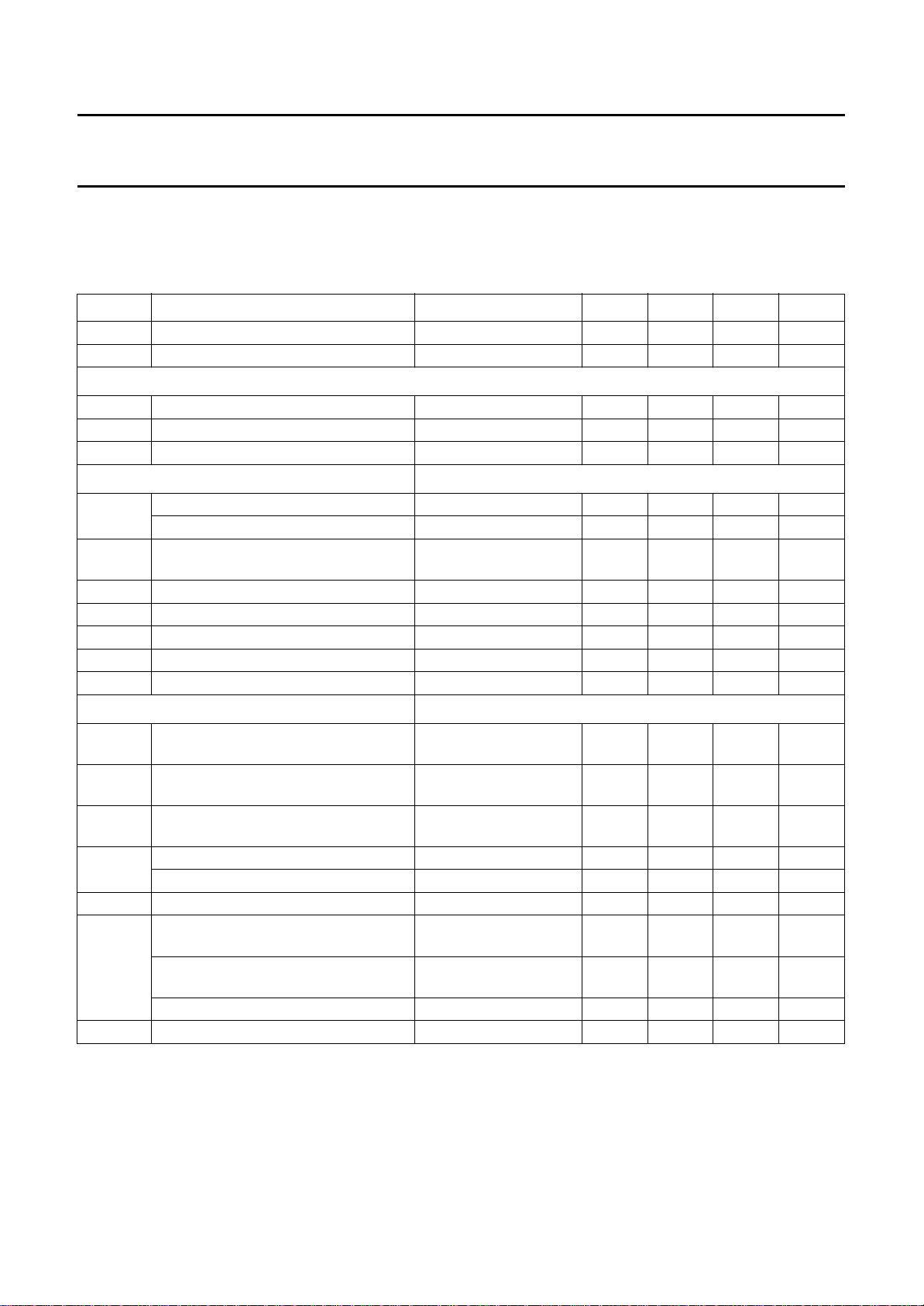
QUICK REFERENCE DATA
SYMBOL PARAMETER MIN. TYP. MAX. UNIT
V
P
I
P
V
i IF
positive supply voltage (pin 20) 4.5 5 8.8 V
supply current 39 46 53 mA
vision IF input signal sensitivity
− 50 90 µV
(RMS value, pins 1 and 2)
maximum vision IF input signal
70 150 − mV
(RMS value, pins 1 and 2)
G
v
V
o CVBS
IF gain control range 64 70 73 dB
CVBS output signal on pin 7 (peak-to-peak value) 1.7 2.0 2.3 V
B −3 dB video bandwidth on pin 7 6 8 − MHz
S/N (W) signal-to-noise ratio weighted; for video 56 59 − dB
α
1.1
α
3.3
α
H
T
amb
intermodulation attenuation 56 62 − dB
56 62 − dB
suppression of harmonics in video signal 35 40 − dB
operating ambient temperature range 0 −+70 °C
ORDERING INFORMATION
EXTENDED
TYPE NUMBER
TDA9803 20 DIL plastic SOT146
TDA9803T 20 mini-pack plastic SOT163A
Note
1. SOT146-1; 1996 December 9.
2. SOT163-1; 1996 December 9.
November 1992 2
PINS
PIN
POSITION
PACKAGE
MATERIAL CODE
(1)
(2)
Philips Semiconductors Preliminary specification
Multistandard VIF-PLL demodulator TDA9803
November 1992 3
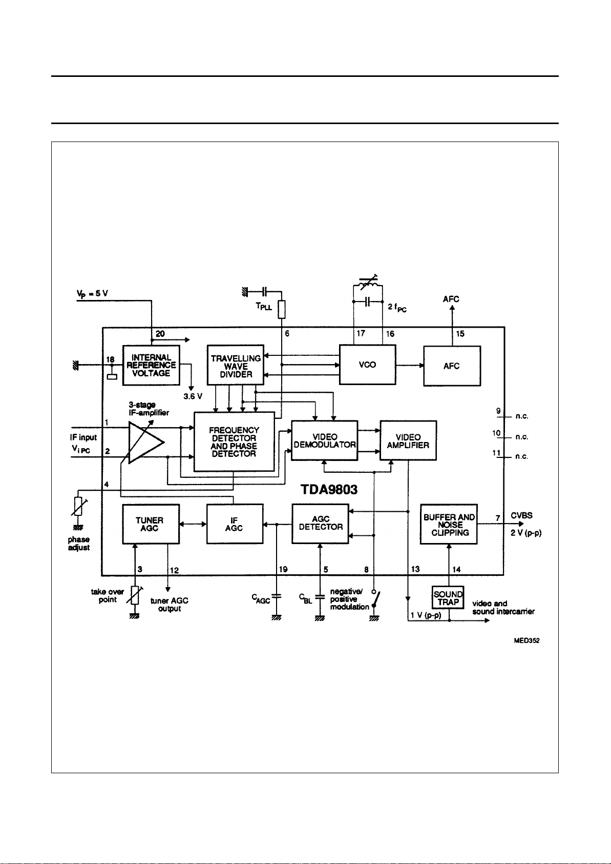
Fig.1 Block diagram.
Philips Semiconductors Preliminary specification
Multistandard VIF-PLL demodulator TDA9803
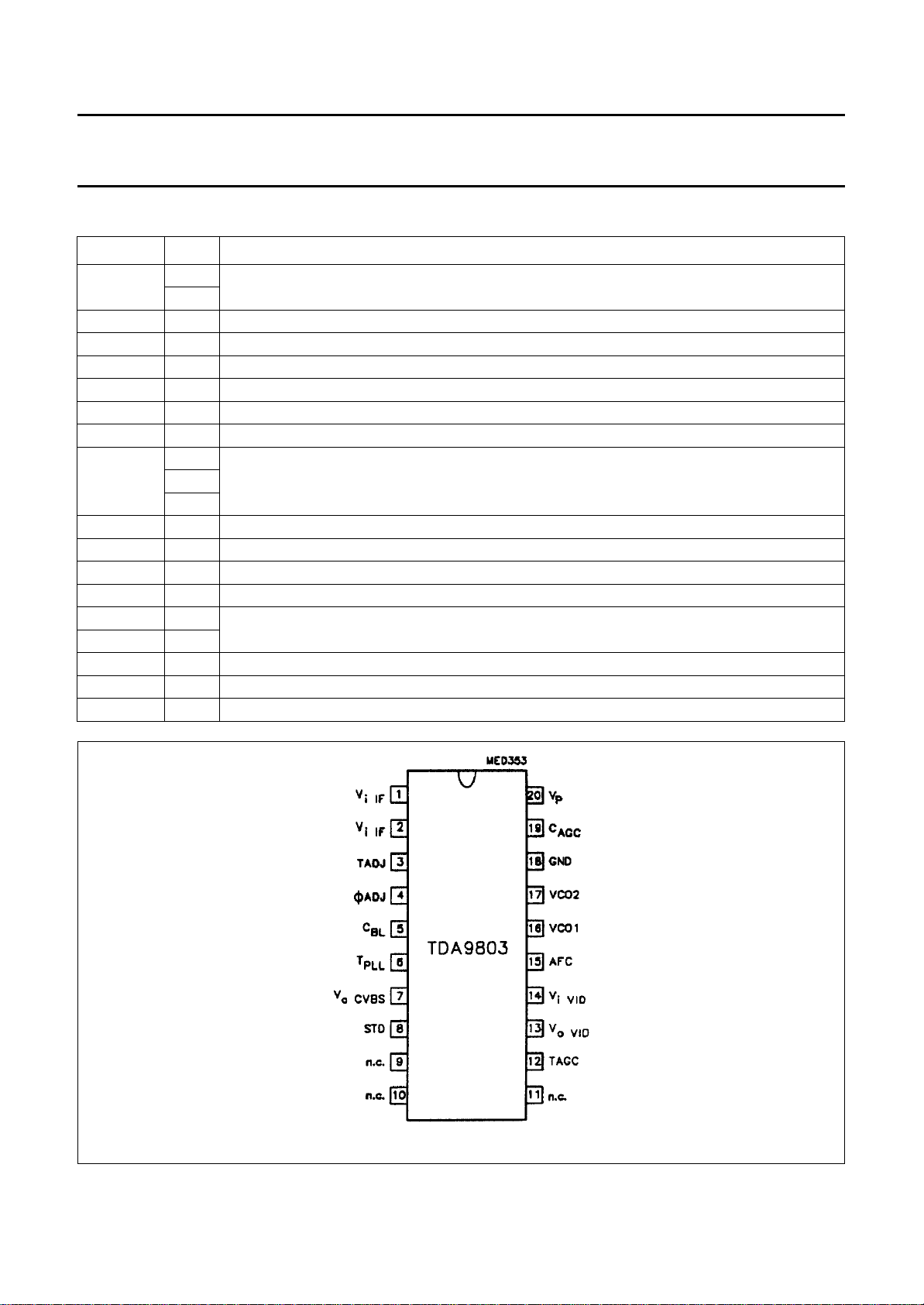
PINNING
SYMBOL PIN DESCRIPTION
V
i IF
TADJ 3 tuner AGC take-over adjust (TOP)
ΦADJ 4 phase detector adjust
C
BL
T
PLL
V
o CVBS
STD 8 standard switch (negative = HIGH, positive = LOW)
n.c. 9 not connected
TAGC 12 tuner AGC output
V
o VID
V
i VID
AFC 15 automatic frequency control output
VCO1 16 VCO reference circuit for 2 f
VCO2 17
GND 18 ground (0 V)
C
AGC
V
P
1 vision IF differential input signal
2
5 black level capacitor, mute switch input
6 PLL time constant of phase detector
7 CVBS (positive) output signal
10
11
13 video and sound intercarrier output signal
14 video input signal to buffer amplifier
PC
19 AGC capacitor
20 positive supply voltage
November 1992 4
Fig.2 Pin configuration.

Philips Semiconductors Preliminary specification
Multistandard VIF-PLL demodulator TDA9803
FUNCTIONAL DESCRIPTION
Vision IF input
The vision IF amplifier consists of three AC-coupled
differential amplifier stages; each stage comprises a
controlled feedback network by means of emitter
degeneration.
IF and tuner AGC
The automatic control voltage to maintain the video output
signal at a constant level is generated according to the
transmission standard. For negative modulation the
peak-sync level is detected, for positive modulation the
peak white level is detected. The AGC detector charges
and discharges the capacitor on pin 19 to set the IF gain
and the tuner gain. The standard is switched by the voltage
on pin 8. To reduce the response time for positive
modulation (which needs a very long time constant) a
black level detector (C
discharge current for low-level video signals.
The AGC capacitor voltage is transferred to an internal IF
control signal, and is fed to the tuner AGC to generate the
tuner AGC output current on pin 12 (open-collector
output). The tuner AGC voltage take over point is adjusted
on pin 3. This allows the tuner and the IF SAW filter to be
matched to achieve the optimum IF input level.
Frequency detector, phase detector and video
demodulator
) increases the AGC capacitor
BL
switched in the demodulator stage according to the TV
standard.
VCO and travelling wave divider
The VCO operates with a symmetrically-connected
reference LC-circuit, operating at double vision carrier
frequency. Frequency control is performed by an internal
varicap diode. The voltage to set the VCO frequency to the
actual frequency of double vision carrier frequency, is also
amplified and converted for the AFC output current.
The VCO signal is divided-by-two in a travelling wave
divider, which generates two differential output signals
with 90 degree phase difference independent of
frequency.
Video amplifier, buffer and noise clipping
The video amplifier is a wide bandwidth operational
amplifier with internal feedback. Dependent on
transmission standard, a level shifter provides the same
sync level for positive as for negative modulation. A
nominal positive modulated video signal of 1 V (p-p) is
present on the composite video output (pin 13).
The input impedance of the 7 dB wideband buffer amplifier
(with internal feedback) is suitable for ceramic sound trap
filters.
The CVBS output (pin 7) provides a positive video signal
of 2 V (p-p). Noise clipping is provided internally.
The IF amplifier output signal is fed to a frequency detector
and to a phase detector. The frequency detector is
operational before lock-in. A DC current is generated
which is proportional to the frequency difference between
the input frequency and the VCO frequency. After lock-in,
the frequency detector and the phase detector generate a
DC current proportional to the phase difference between
VCO and input signals. The control signal for the VCO is
provided by the phase detector. The video demodulator is
a linear multiplier, designed for low distortion and wide
bandwidth. The vision IF input signal is multiplied by the
in-phase component of the VCO output. The demodulated
output signal is fed via an integrated low-pass filter
= 12 MHz) to the video amplifier for suppression of the
(f
g
carrier harmonics. The polarity of the video signal is
November 1992 5
Philips Semiconductors Preliminary specification
Multistandard VIF-PLL demodulator TDA9803
LIMITING VALUES
In accordance with the Absolute Maximum Rating System (IEC134)
SYMBOL PARAMETER MIN. MAX. UNIT
V
P
V
I
t
s max
V
12
T
stg
V
ESD
Notes
1. Supply current I
2. Equivalent to discharging a 200 pF capacitor through a 0 Ω series resistor (negative and positive voltage).
supply voltage (pin 20) for a maximum chip
temperature (note 1)
SOT146 at +120 °C 0 8.8 V
SOT163A at +100 °C 0 5.5 V
voltage on pins 1, 2, 7, 8, 13, 14, 15 and 19 0 V
P
short−circuit time − 10 s
tuner AGC output voltage − 13.2 V
storage temperature range −25 +150 °C
electrostatic handling for all pins (note 2) −±300 V
= 53 mA at T
P
amb
= +70 °C.
V
THERMAL RESISTANCE
SYMBOL PARAMETER THERMAL RESISTANCE
R
th j-a
from junction to ambient in free air
SOT146 73 K/W
SOT163A 85 K/W
November 1992 6
Philips Semiconductors Preliminary specification
Multistandard VIF-PLL demodulator TDA9803
CHARACTERISTICS
= 5 V; T
V
P
(sync level at B/G; peak-white level at L); video modulation DSB; residual carrier: B/G = 10%, L = 3%; video signal in
accordance with CCIR line 17; measurements taken in Fig.3 unless otherwise specified
SYMBOL PARAMETER CONDITIONS MIN. TYP. MAX. UNIT
V
P
I
P
Standard switch (pin 8)
V
IH
V
IL
I
IL
Vision IF input (pins 1 and 2)
V
i
∆V
i
G
IF
B −3 dB IF bandwidth upper cut-off frequency 70 100 − MHz
R
i
C
i
V
1, 2
True synchronous video demodulator
f
VCO
∆f
VCO
V
o ref
∆f
PC
t
acqu
V
i IF
l
loop
= +25 °C; fPC= 38.9 MHz; fSC= 33.4 MHz with VPC/VSC= 13 dB (B/G); V
amb
= 10 mV RMS value
iIF
supply voltage range (pin 20) see note 1 4.5 5 8.8 V
supply current 39 46 53 mA
input voltage for negative modulation see note 2 1.5 − V
P
V
input voltage for positive modulation 0 − 0.8 V
LOW level input current V8= 0 V −−300 −360 µA
B/G standard
input signal sensitivity (RMS value) −1 dB video at output − 50 90 µV
maximum input signal (RMS value) +1 dB video at output 70 150 − mV
IF amplitude difference between
within AGC range − 0.7 1 dB
picture and sound carrier
IF gain control range see Fig.4 64 70 73 dB
input resistance 1.7 2.2 2.7 kΩ
input capacitance 1.2 1.7 2.5 pF
DC input voltage 3.0 3.4 3.8 V
see note 3
maximum oscillator frequency for
f = 2f
PC
125 130 − MHz
carrier regeneration
oscillator drift (free running) as a
function of temperature
oscillator swing at pins 16 and 17
see note 4;
∆T = 0 to +70 °C
−−±1300 10
tbn 120 tbn mV
(RMS value)
vision carrier capture range (negative) 1.5 2 − MHz
vision carrier capture range (positive) 1.5 2 − MHz
acquisition time see note 5; BL = 60 kHz −−30 ms
IF input signal sensitivity
(RMS value, pins 1 and 2)
for PLL still locked see note 6;
− 70 100 µV
maximum IF gain
for C/N = 10 dB see note 7 − 100 140 µV
FPLL loop offset current at pin 6 see note 8 −−±4.5 µA
−6
November 1992 7
 Loading...