

Philips TDA9801T, TDA9801 Datasheet

INTEGRATED CIRCUITS
DATA SH EET
TDA9801
Single standard VIF-PLL
demodulator and FM-PLL detector
Product specification
Supersedes data of 1998 May 06
File under Integrated Circuits, IC02
1999 Aug 26

Philips Semiconductors Product specification
Single standard VIF-PLL demodulator
and FM-PLL detector
FEATURES
• Suitable for negative vision modulation
• Applicable for IF frequencies of 38.9, 45.75 and
58.75 MHz
• Gain controlled wide-band Vision Intermediate
Frequency (VIF) amplifier (AC-coupled)
• True synchronous demodulation with active carrier
regeneration (ultra-linear demodulation, good
intermodulation figures, reduced harmonics and
excellent pulse response)
• Peak sync pulse AGC
• Video amplifier to match sound trap and sound filter
• AGC output voltage for tuner with fixed resistor for
takeover point setting
• AFC detector without extra reference circuit
• Alignment-free FM-PLL detector with high linearity
TDA9801
• Stabilizer circuit for ripple rejection and to achieve
constant output signals
• 5 to 9 V positive supply voltage range
• Low power consumption of 300 mW at 5 V supply
voltage.
GENERAL DESCRIPTION
TheTDA9801(T)isamonolithicintegratedcircuitforvision
and sound IF signal processing in TV and VTR sets and
multimedia front-ends.
ORDERING INFORMATION
TYPE NUMBER
NAME DESCRIPTION VERSION
TDA9801 DIP20 plastic dual in-line package; 20 leads (300 mil) SOT146-1
TDA9801T SO20 plastic small outline package; 20 leads; body width 7.5 mm SOT163-1
PACKAGE
1999 Aug 26 2

Philips Semiconductors Product specification
Single standard VIF-PLL demodulator
TDA9801
and FM-PLL detector
QUICK REFERENCE DATA
SYMBOL PARAMETER CONDITIONS MIN. TYP. MAX. UNIT
V
P
I
P
V
i(sens)(VIF)(rms)
V
i(max)(rms)
G
IF
V
o(CVBS)(p-p)
B
v(−3dB)
S/N
W
α
IM(0.92/1.1)
α
IM(2.76/3.3)
α
H(sup)
V
o(AF)(max)(rms)
T
amb
supply voltage note 1 4.5 5.0 9.9 V
supply current VP= 9 V 52 61 70 mA
sensitivity of VIF input signal
(RMS value)
maximum input voltage
(RMS value)
−1 dB video at output;
fPC= 38.9 or 45.75 MHz
+1 dB video at output;
fPC= 38.9 or 45.75 MHz
− 50 90 µV
70 150 − mV
IF gain control fPC= 38.9 or 45.75 MHz 64 70 dB
CVBS output voltage
VP= 5 V 1.7 2.0 2.3 V
(peak-to-peak value)
−3 dB video bandwidth CL< 20 pF; RL>1kΩ 68−MHz
weighted signal-to-noise ratio VP= 5 V; note 2 56 60 − dB
intermodulation attenuation at
for BLUE 56 62 − dB
f = 0.92 or 1.1 MHz
intermodulation attenuation at
for BLUE 56 62 − dB
f = 2.76 or 3.3 MHz
harmonics suppression in video
note 3 35 40 − dB
signal
maximum output AF signal
THD < 1.5% 0.8 −−V
handling voltage (RMS value)
ambient temperature −20 − +70 °C
Notes
1. Values of video and sound parameters can be decreased at V
= 4.5 V.
P
2. S/N is the ratio of the black-to-white amplitude to the black level noise voltage (RMS value) at pin CVBS.
B = 5 MHz weighted in accordance with
3. Measurements taken with SAW filter G1962; VSB modulation; f
“CCIR 567”
at a source impedance of 50 Ω.
> 0.5 MHz; loop bandwidth BL = 60 kHz.
video
1999 Aug 26 3
This text is here in white to force landscape pages to be rotated correctly when browsing through the pdf in the Acrobat reader.This text is here in
a
_white to force landscape pages to be rotated correctly when browsing through the pdf in the Acrobat reader.This text is here inThis text is here in
white to force landscape pages to be rotated correctly when browsing through the pdf in the Acrobat reader. white to force landscape pages to be ...
TPLL
6
ndbook, full pagewidth
2f
PC
17
16
AFC
15
1999 Aug 26 4
VP = 5 V (9 V)
V
P VCO2 VCO1
20
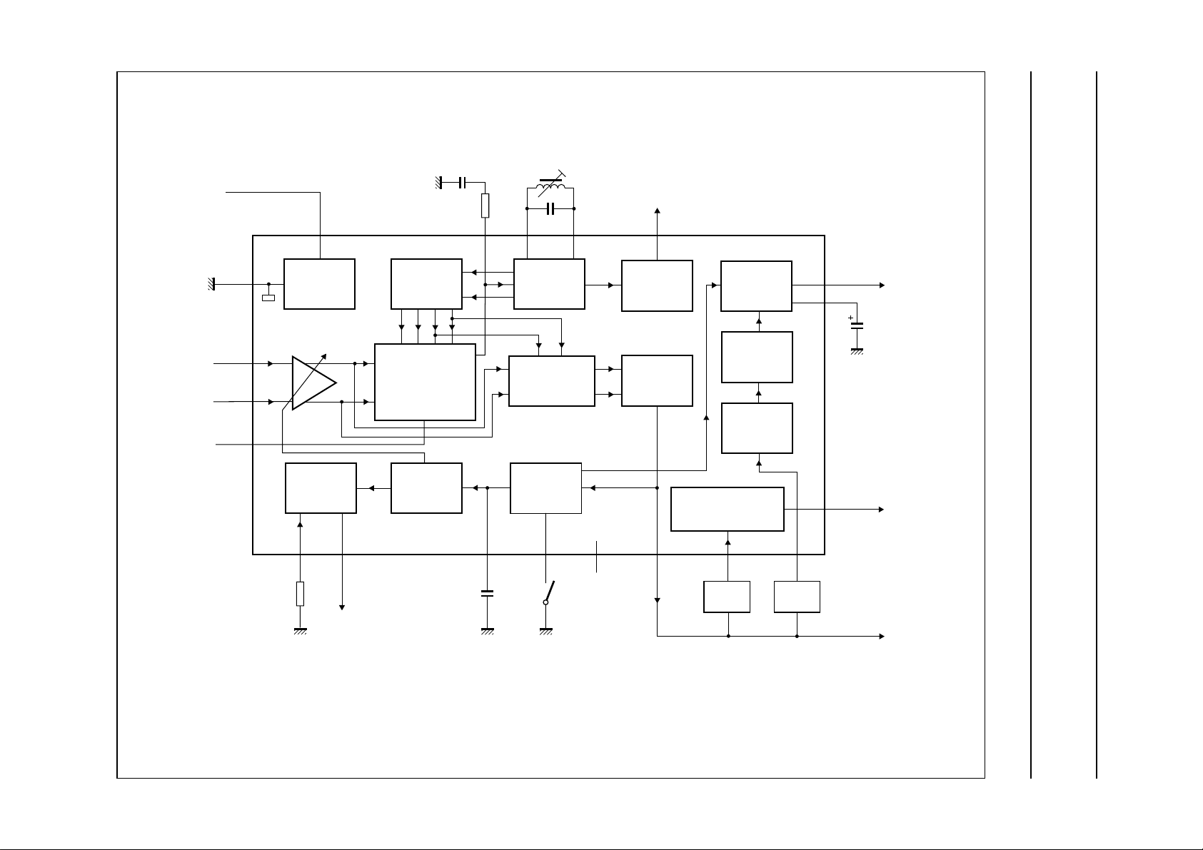
BLOCK DIAGRAM
Philips Semiconductors Product specification
Single standard VIF-PLL demodulator
and FM-PLL detector
GND
VIF1
VIF2
ADJ
18
1
2
4
takeover
point
INTERNAL
REFERENCE
VOLTAGE
3-STAGE
IF-AMPLIFIER
TUNER
AGC
3
R
TOP
tuner AGC
TRAVELLING
WAVE
DIVIDER
FREQUENCY
DETECTOR
AND PHASE
DETECTOR
VCO
VIDEO
DEMODULATOR
AFC
DETECTOR
VIDEO
AMPLIFIER
TDA9801
sound
mute
IF
AGC
12
TAGCTOP
19
DETECTOR
C
AGC
AGC
5
sound
mute
switch
8
n.c.
BUFFER AMPLIFIER
AND NOISE CLIPPER
13
1 V (p-p)
AMPLIFIER
DETECTOR
AMPLIFIER
14
SOUND
TRAP
AF
FM-PLL
LIMITER
SOUND
FILTER
9
10
7
11
SIVIVSOMUTEAGC
AF
DAF
CVBS
2 V (p-p)
video and
intercarrier
MHA879
C
DAF
TDA9801
Fig.1 Block diagram.
Philips Semiconductors Product specification
Single standard VIF-PLL demodulator
and FM-PLL detector
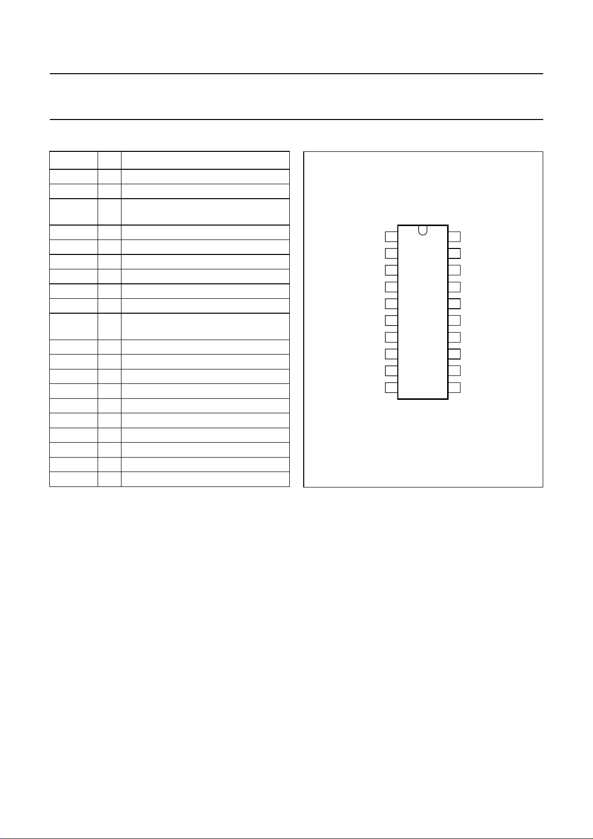
PINNING
SYMBOL PIN DESCRIPTION
VIF1 1 VIF differential input 1
VIF2 2 VIF differential input 2
TOP 3 tuner AGC TakeOver Point (TOP)
connection
ADJ 4 phase adjust connection
MUTE 5 sound mute switch connection
TPLL 6 PLL time constant connection
CVBS 7 CVBS (positive) video output
n.c. 8 not connected
AF 9 AF output
DAF 10 AF amplifier decoupling capacitor
connection
SI 11 sound intercarrier input
TAGC 12 tuner AGC output
VSO 13 video and sound intercarrier output
VI 14 buffer amplifier video input
AFC 15 AFC output
VCO1 16 VCO1 reference circuit for 2f
VCO2 17 VCO2 reference circuit for 2f
GND 18 ground supply (0 V)
AGC 19 AGC detector capacitor connection
V
P
20 supply voltage (+5 V)
PC
PC
handbook, halfpage
1
VIF1
2
VIF2
3
TOP
4
ADJ
MUTE
5
TDA9801
6
TPLL
7
CVBS
8
n.c.
9
AF
10
DAF
MHA880
Fig.2 Pin configuration.
TDA9801
V
20
P
19
AGC
18
GND
17
VCO2
16
VCO1
AFC
15
VI
14
VSO
13
TAGC
12
11
SI
1999 Aug 26 5

Philips Semiconductors Product specification
Single standard VIF-PLL demodulator
and FM-PLL detector
FUNCTIONAL DESCRIPTION
3-stage IF amplifier
The VIF amplifier consists of three AC-coupled differential
amplifier stages (see Fig.1). Each differential stage
comprises a feedback network controlled by emitter
degeneration.
AGC detector, IF AGC and tuner AGC
The automatic control voltage to maintain the video output
signal at a constant level is generated in accordance with
the transmission standard. Since the TDA9801(T) is
suitable for negative modulation only the peak sync pulse
level is detected.
TheAGCdetectorchargesanddischargescapacitorC
to set the IF amplifier and tuner gain. The voltage on
capacitor C
signal, and is fed to the tuner AGC to generate the tuner
AGC output current on pin TAGC (open-collector output).
The tuner AGC takeover point level is set at pin TOP. This
allows the tuner to be matched to the SAW filter in order to
achieve the optimum IF input level.
is transferred to an internal IF control
AGC
AGC
TDA9801
The voltage to set the VCO frequency to the actual double
vision carrier frequency isalso amplified and converted for
the AFC output current.
The VCO signal is divided-by-2 with a Travelling Wave
Divider (TWD) which generates two differential output
signals with a 90 degree phase difference independent of
the frequency.
Video amplifier
The composite video amplifier is a wide bandwidth
operational amplifier with internal feedback. A nominal
positive video signal of 1 V (p-p) is present at pin VSO.
Buffer amplifier and noise clipper
The input impedance of the 7 dB wideband CVBS buffer
amplifier (with internal feedback) is suitable for ceramic
sound trap filters. Pin CVBS provides a positive video
signal of 2 V (p-p). Noise clipping is provided internally.
Sound demodulation
LIMITER AMPLIFIER
Frequency detector and phase detector
The VIF amplifier output signal is fed into a frequency
detector and into a phase detector. During acquisition the
frequency detector produces a DC current proportional to
the frequency difference between the input and the VCO
signal. After frequency lock-in the phase detector
produces a DC current proportional to the phase
difference between the VCO and the input signal. The DC
current of either frequency detector or phase detector is
converted into a DC voltage via the loop filter which
controls the VCO frequency.
Video demodulator
The true synchronous video demodulator is realized by a
linear multiplier which is designed for low distortion and
widebandwidth.ThevisionIFinputsignalis multiplied with
the ‘in phase’ component of the VCO output.
The demodulator output signal is fed via an integrated
low-pass filter (fg= 12 MHz) for suppression of the carrier
harmonics to the video amplifier.
VCO, AFC detector and travelling wave divider
The VCO operates with a symmetrically connected
reference LC circuit, operating at the double vision carrier
frequency. Frequency control is performed by an internal
variable capacitor diode.
The FM sound intercarrier signal is fed to pin SI and
through a limiter amplifier before it is demodulated.
The result is high sensitivity and AM suppression.
The limiter amplifier consists of 7 stages which are
internally AC-coupled in order to minimizing the DC offset.
FM-PLL DETECTOR
The FM-PLL demodulator consists of an RC oscillator,
loop filter and phase detector. The oscillator frequency is
locked on the FM intercarrier signal from the limiter
amplifier. As a result of this locking, the RC oscillator is
frequency modulated. The modulating voltage (AF signal)
is used to control the oscillator frequency. By this, the
FM-PLL operates as an FM demodulator.
AF AMPLIFIER
The audio frequency amplifier with internal feedback is
designed for high gain and high common-mode rejection.
The low-level AF signal output from the FM-PLL
demodulator is amplified and buffered in a low-ohmic
audiooutput stage. An external decouplingcapacitor C
removes the DC voltage from the audio amplifier input.
By using the sound mute switch (pin MUTE) the AF
amplifier is set in the mute state.
DAF
1999 Aug 26 6

Philips Semiconductors Product specification
Single standard VIF-PLL demodulator
TDA9801
and FM-PLL detector
LIMITING VALUES
In accordance with the Absolute Maximum Rating System (IEC 134).
SYMBOL PARAMETER CONDITIONS MIN. MAX. UNIT
V
P
V
n
t
sc(max)
T
stg
T
amb
V
es
Notes
1. Machine model class B (L = 2.5 µH).
supply voltage IP= 70 mA; T
amb
=70°C;
maximum chip temperature
125 °C for TDA9801 0 9.9 V
128 °C for TDA9801T 0 9.9 V
voltage on
pins VIF1, VIF2, AFC and AGC 0 V
P
V
pin TAGC − 13.2 V
maximum short-circuit time to ground or V
P
− 10 s
storage temperature −25 +150 °C
ambient temperature −20 +70 °C
electrostatic handling voltage note 1 −300 +300 V
THERMAL CHARACTERISTICS
SYMBOL PARAMETER CONDITIONS VALUE UNIT
R
th(j-a)
thermal resistance from junction to ambient in free air
TDA9801 73 K/W
TDA9801T 85 K/W
CHARACTERISTICS
VP=5V; T
=25°C; see Table 1 for input frequencies and picture-to-sound carrier ratios; V
amb
i(VIF)(rms)
= 10 mV (sync
pulse level); IF input from 50 Ω via broadband transformer 1 : 1; DSB video modulation; 10% residual carrier; video
signal in accordance with
“CCIR, line 17”
or
“NTC-7 Composite”
; measurements taken in test circuit of Fig.12; unless
otherwise specified.
SYMBOL PARAMETER CONDITIONS MIN. TYP. MAX. UNIT
Supply: pin V
V
P
I
P
P
supply voltage note 1 4.5 5.0 9.9 V
supply current VP= 5 V 51 60 70 mA
V
= 9 V 52 61 70 mA
P
Vision IF input: pins VIF1 and VIF2
V
i(sens)(VIF)(rms)
V
i(max)(rms)
V
I
sensitivity of VIF input
voltage (RMS value)
maximum VIF input voltage
(RMS value)
−1 dB video at output
= 38.9 or 45.75 MHz − 50 90 µV
f
PC
f
= 58.75 MHz − 60 100 µV
PC
1 dB video at output
f
= 38.9 or 45.75 MHz 70 150 − mV
PC
f
= 58.75 MHz 80 160 − mV
PC
DC input voltage 3.0 3.4 3.8 V
1999 Aug 26 7

Philips Semiconductors Product specification
Single standard VIF-PLL demodulator
TDA9801
and FM-PLL detector
SYMBOL PARAMETER CONDITIONS MIN. TYP. MAX. UNIT
∆V
int
G
IF
B
IF(−3dB)
R
i(dif)
C
i(dif)
VCO and video demodulator; note 3
f
VCO(max)
/∆T VCO frequency variation
∆f
VCO
V
VCO(rms)
f
cr(PC)
t
acq
V
i(sens)(VIF)(rms)
I
offset(TPLL)
Video amplifier output (sound carrier off): pin VSO
V
o(VSO)(p-p)
V
sync
V
v(clu)
V
v(cll)
V
o(intc)(rms)
R
o
I
bias
internal IF amplitude
within AGC range − 0.7 1 dB
difference between picture
and sound carrier
IF gain control see Fig.6
= 38.9 or 45.75 MHz 64 70 − dB
f
PC
f
= 58.75 MHz 62 68 − dB
PC
−3 dB IF bandwidth upper limit cut-off
70 100 − MHz
frequency
differential input resistance note 2 1.7 2.2 2.7 kΩ
differential input
note 2 1.2 1.7 2.5 pF
capacitance
maximum VCO frequency for carrier regeneration;
f=2f
PC
with temperature
VCO voltage swing
(RMS value)
picture carrier capture
frequency range
free running; I
note 4
measured between
pins VCO1 and VCO2
= 38.9 MHz − 120 − mV
f
PC
f
= 45.75 MHz − 100 − mV
PC
f
= 58.75 MHz − 80 − mV
PC
negative 1.4 1.8 − MHz
positive 1.4 1.8 − MHz
AFC
=0;
125 130 − MHz
−−±20 × 10−6K
acquisition time BL = 60 kHz; note 5 −−30 ms
sensitivity of VIF input
(RMS value)
PLL still locked;
maximum IF gain; note 6
− 50 90 µV
C/N = 10 dB; note 7 − 100 140 µV
offset current at pin TPLL note 8 −−±2.0 µA
VSO output voltage
(peak-to-peak value)
see Fig.5
V
= 5 V 0.90 1.0 1.25 V
P
V
= 9 V 0.95 1.1 1.25 V
P
sync pulse voltage level 1.35 1.5 1.6 V
upper video clipping
VP− 1.1 VP− 1 − V
voltage level
lowervideo clipping voltage
− 0.7 0.9 V
level
intercarrier output voltage
sound carrier on; note 9 − 32 − mV
(RMS value)
output resistance note 2 −−10 Ω
DC bias current for internal emitter-follower
1.8 2.5 − mA
at pin VSO
−1
1999 Aug 26 8

Philips Semiconductors Product specification
Single standard VIF-PLL demodulator
TDA9801
and FM-PLL detector
SYMBOL PARAMETER CONDITIONS MIN. TYP. MAX. UNIT
I
o(sink)(max)
I
o(source)(max)
B
v(−3dB)
α
H(sup)
PSRR
VSO
Buffer amplifier and noise clipper input: pin VI
R
i
C
i
V
I
Buffer amplifier output: pin CVBS
G
v
B
v(−3dB)
V
o(v)(p-p)
V
v(clu)
V
v(cll)
V
sync
R
o
I
bias
I
o(sink)(max)
I
o(source)(max)
Measurements from VIF inputs to CVBS output (330 Ω connected between pins VSO and VI, sound carrier off)
V
o(CVBS)(p-p)
∆V
o(CVBS)
∆V
o(bl)
G
dif
ϕ
dif
B
v(−3dB)
maximum AC and DC
1.4 −− mA
output sink current
maximum AC and DC
2.0 −− mA
output source current
−3 dB video bandwidth CL< 50 pF; RL>1kΩ 710− MHz
harmonics suppression in
video signal
power supply ripple
CL< 50 pF; RL>1kΩ;
35 40 − dB
note 10
see Fig.7 32 35 − dB
rejection at pin VSO
input resistance 2.6 3.3 4.0 kΩ
input capacitance 1.4 2 3.0 pF
DC input voltage pin VI not connected 1.5 1.8 2.1 V
voltage gain note 11 6 7 7.5 dB
−3 dB video bandwidth CL< 20 pF; RL>1kΩ 811− MHz
video output voltage
(peak-to-peak value)
upper video clipping
sound carrier off;
see Fig.12
1.7 2.0 2.3 V
3.9 4.0 − V
voltage level
lowervideo clipping voltage
− 1.0 1.1 V
level
sync pulse voltage level − 1.35 − V
output resistance −−10 Ω
DC bias current internal emitter-follower at
1.8 2.5 − mA
pin CVBS
maximum AC and DC
1.4 −− mA
output sink current
maximum AC and DC
2.4 −− mA
output source current
CVBS output voltage
(peak-to-peak value)
deviation of CVBS output
voltage
VP= 5 V 1.7 2.0 2.3 V
= 9 V 1.8 2.2 2.6 V
V
P
at B/G standard
50 dB gain control −−0.5 dB
30 dB gain control −−0.1 dB
black level tilt gain variation; note 12 −−1%
differential gain
“CCIR, line 330”
or
− 25 %
“NTC-7 Composite”
differential phase
“CCIR, line 330”
or
− 2 4 deg
“NTC-7 Composite”
−3 dB video bandwidth CL< 20 pF; RL>1kΩ 68− MHz
1999 Aug 26 9

Philips Semiconductors Product specification
Single standard VIF-PLL demodulator
TDA9801
and FM-PLL detector
SYMBOL PARAMETER CONDITIONS MIN. TYP. MAX. UNIT
S/N
W
α
IM(0.92/1.1)
α
IM(2.76/3.3)
∆V
r(PC)(rms)
α
H(sup)
PSRR
CVBS
AGC detector output: pin AGC
t
res
I
ch
I
dch
V
o
Tuner AGC
V
i(VIF)(rms)
QV
i(VIF)(rms)
/∆T variation of tuner takeover
∆V
i(VIF)
∆G
IF
weighted signal-to-noise
ratio
intermodulation attenuation
at f = 0.92 or 1.1 MHz
see Fig.3; note 13
V
=5V 56 60 − dB
P
V
=9V 55 59 − dB
P
see Fig.4; note 14
for BLUE 56 62 − dB
for YELLOW 58 64 − dB
intermodulation attenuation
at f = 2.76 or 3.3 MHz
see Fig.4; note 14
for BLUE 56 62 − dB
for YELLOW 57 63 − dB
residual picture carrier
(RMS value)
harmonics suppression in
fundamental wave − 110 mV
harmonics − 110 mV
note 10 35 40 − dB
video signal
power supply ripple
see Fig.7 25 28 − dB
rejection at pin CVBS
response time at 50 dB amplitude step of
input signal
for increasing step − 110 ms
for decreasing step − 50 100 ms
charging current note 12 0.82 1.1 1.38 mA
discharging current 16 22 28 µA
gain control output voltage see Fig.6
maximum gain 0 −− V
VIF input voltage
(RMS value)
accuracy level of tuner
takeover point (RMS value)
minimum gain −−V
for onset tuner takeover
point
minimum level with
R
=22kΩ
TOP
maximum level with
=0Ω
R
TOP
R
=13kΩ;
TOP
I
= 0.4 mA
TAGC
I
= 0.4 mA − 0.02 0.06 dB/K
TAGC
−−5mV
50 −− mV
7 − 14 mV
−0.7 V
P
point with temperature
IF slip by automatic gain
control
tuner gain current from
20 to 80%
− 68 dB
1999 Aug 26 10
 Loading...