

Philips tda9725 DATASHEETS
INTEGRATED CIRCUITS
DATA SH EET
TDA9725
Y/C automatic adjustment
processor (VHS standard)
Product specification
Supersedes data of 1995 Dec 06
File under Integrated Circuits, IC02
1996 Oct 14
Philips Semiconductors Product specification
Y/C automatic adjustment processor
TDA9725
(VHS standard)
FEATURES
• Automatic adjustment by control loops
• Integrated filters
• Simple SVHS playback
• Colour sequence correction for long-play still mode
• Automatic gain control for FM.
QUICK REFERENCE DATA
SYMBOL PARAMETER CONDITIONS MIN. TYP. MAX. UNIT
V
I
V
CC
CC
i(p-p)
supply voltage 4.5 5.0 5.5 V
supply current VCC= 5 V; playback 140 170 200 mA
video input voltage; CVBS signal
(peak-to-peak value)
V
oREC(p-p)
video output record voltage
(peak-to-peak value)
V
oPB(p-p)
video output playback voltage
(peak-to-peak value)
V
iFM(p-p)
V
oFM(p-p)
V
CFT(p-p)
FM input voltage (peak-to-peak value) FM AGC active 63 200 632 mV
FM output voltage (peak-to-peak value) RL=1kΩ 0.7 0.9 1.1 V
chrominance input voltage (+FM) from tape
(peak-to-peak value)
V
CTT(p-p)
chrominance output voltage to tape
(peak-to-peak value)
T
stg
T
amb
storage temperature −25 − +150 °C
operating ambient temperature −20 − +70 °C
GENERAL DESCRIPTION
The TDA9725 is an integrated circuit for chrominance and
luminance processing (record and playback) in VHS tape
recorders for PAL, SECAM/ME and NTSC systems
(4.43 MHz playback only) with internal filter and without
adjustments.
0.6 1.0 2.0 V
video/sync = 7/3 2.03 2.14 2.25 V
video/sync = 7/3;
2.03 2.14 2.25 V
nominal FM signal
11 110 310 mV
467 660 932 mV
ORDERING INFORMATION
TYPE
NUMBER
NAME DESCRIPTION VERSION
PACKAGE
TDA9725 SDIP52 plastic shrink dual in-line package; 52 leads (600 mil) SOT247-1
1996 Oct 14 2
Philips Semiconductors Product specification
Y/C automatic adjustment processor
(VHS standard)
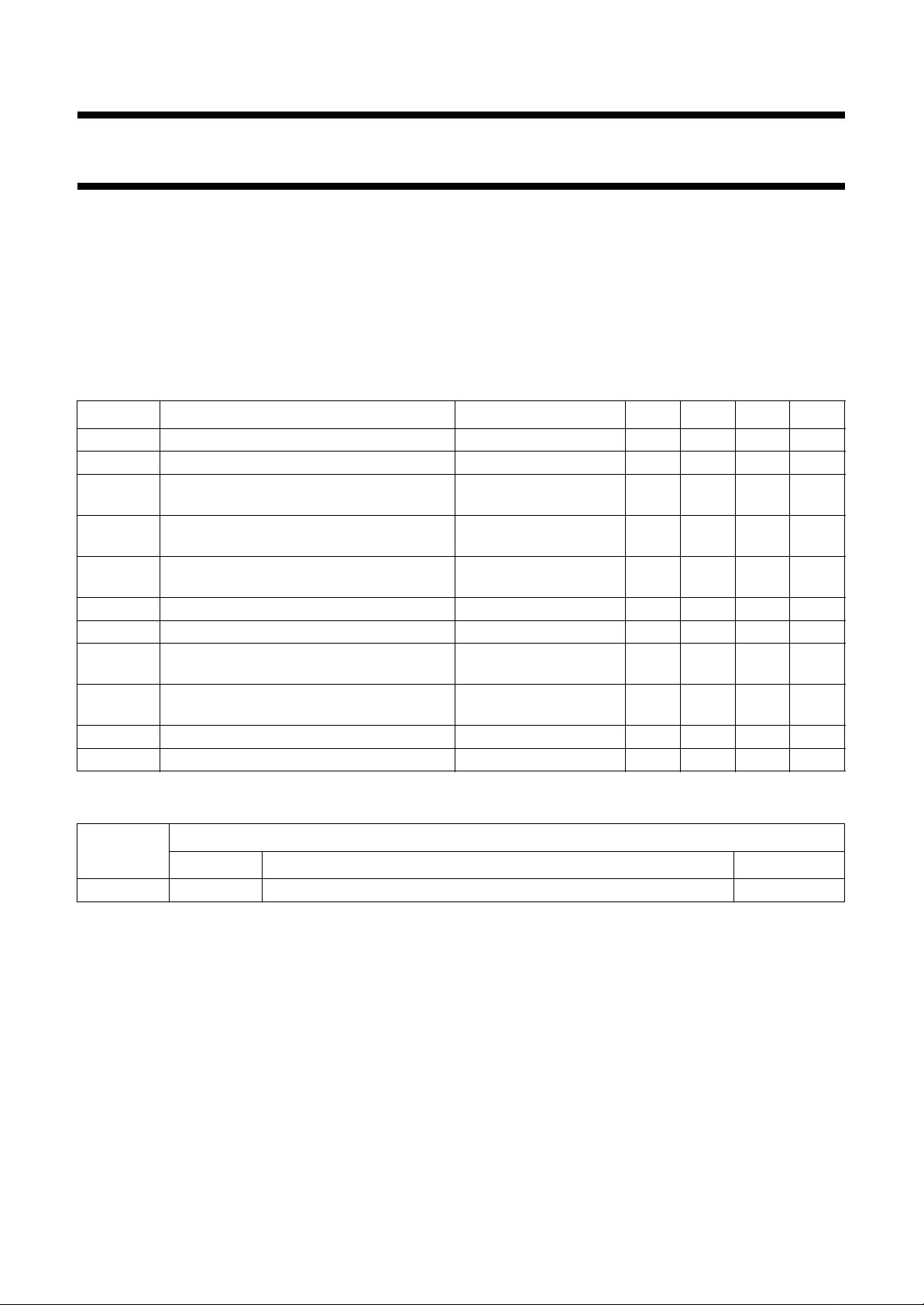
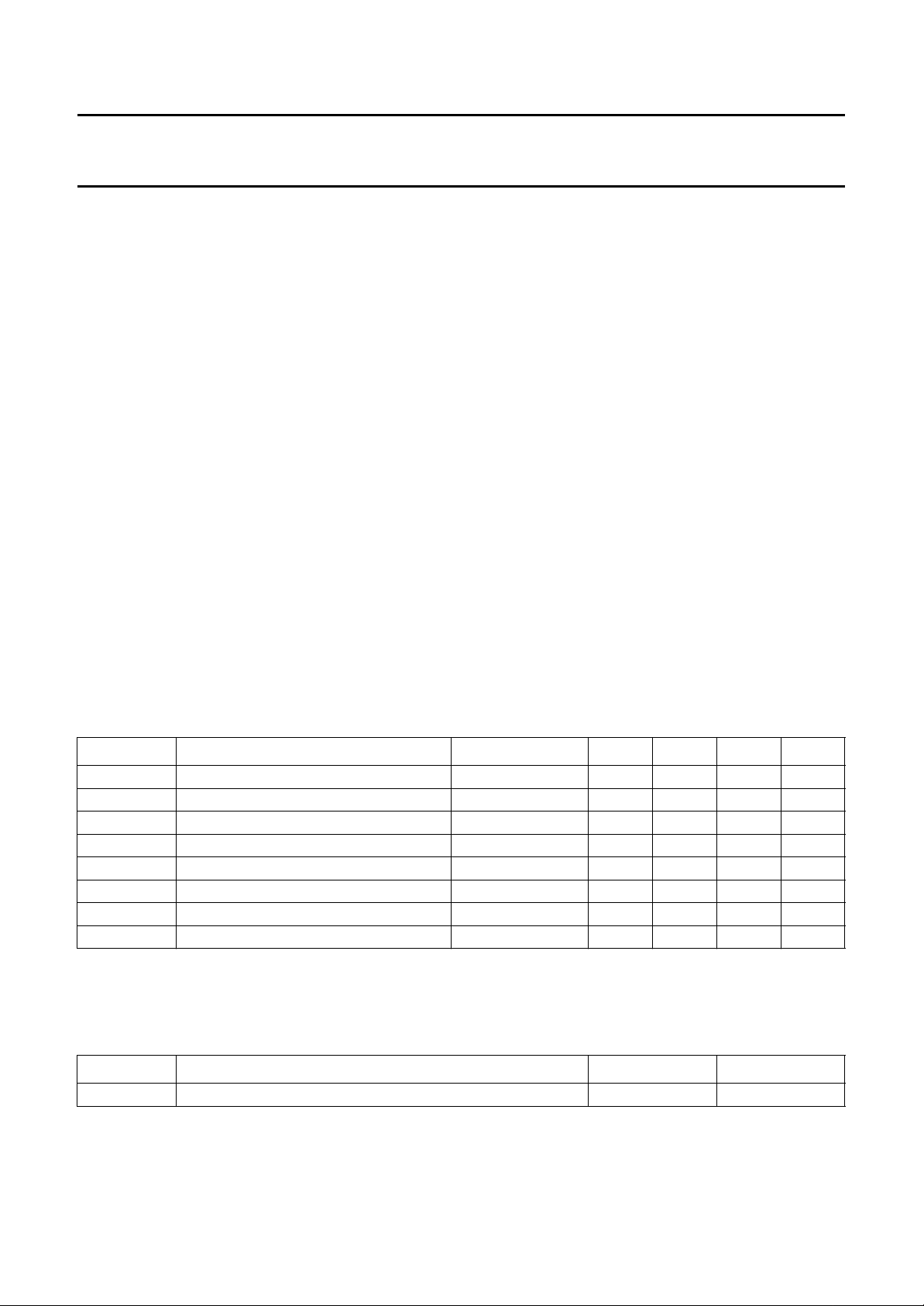
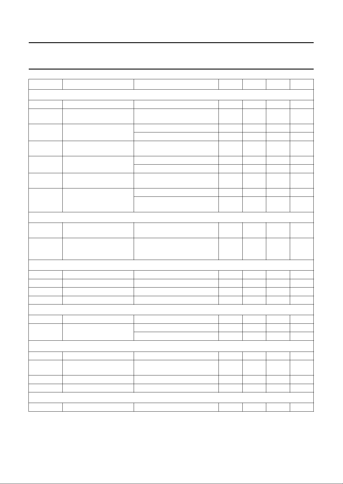
BLOCK DIAGRAM
handbook, full pagewidth
LPNC
GND(Y)
C
CCD
1.3
kΩ
10
µF
47
nF
52 51 50 49 48 47 46 45 44 43 42 41 40
VTC
1HDL
CCD
CCD
AGC
CLAMP
2
1 µF
VFC
50 kΩ
C
YNR
SS
CLAMP
1
YNR
PROCESSOR
22 nF
SYNC
SYNC
SEPARATOR
DOP
MIXER
YNR
CVBSI
C
AGC
4.7 µF 4.7 µF
HSS
AGC
AGC
DETECTOR
CLPA
Y/C
MIXER
to BPF 4.43
REC
PB
SCL
REC
LPF
TDA9725
0.1
µF
V
CC(Y)
22
10
µH
µF
A
CVBSO
CHI
PB
NOISE
CLIP
50
kΩ
CHARACTER
INSERT
EDIT
EDIT
50 kΩ
1.6 V
12 34 5 6 7 8 9 10 11 12 13 14
4.7
µF
(1)
PCTL
TP2
CDEV
EDIT
25 kΩ
DEVIATION/PLAYBACK
DETECTOR
ME
SQPB
1 kΩ
270 Ω
1 nF
SQPB
5%
NFB
NOISE
CANCELLER
1
PICTURE
to pin 6
CLPB
W/DC
to CLP3
22
nF
C
CLP3
CLAMP
DEVIATION
CONTROL
REC
PB
MODULATOR
0.1 µF
C
F0E
NLDE
YLPF
NLE
REC
PB
3
470 Ω
680 pF
peaking
DTE
SQPB
FM DEMODULATOR
SUBLPF
MDEBMDECMEO
1.5 kΩ1.5 kΩ
5%
f
PROCESSOR
0.1
µF
PB
REC
PB
TDA9725
2.5 dB
0
DOUBLE
LIMITER
PB
1 kΩ
FMO
V
CC(FM)
DROP-OUT
DETECTOR
ENVELOPE
DETECTOR
50 kΩ
PTR
pin 14
HIGH
0.01
µF
FM
AGC
FMI
GATE
C
FMA
DOP
0.33
µF
MGB694
(1) Low leakage current.
All capacitors for loop filter ±10%; all other capacitors+10%/−50%; all resistors ±5%; all inductors ±10%; unless otherwise specified.
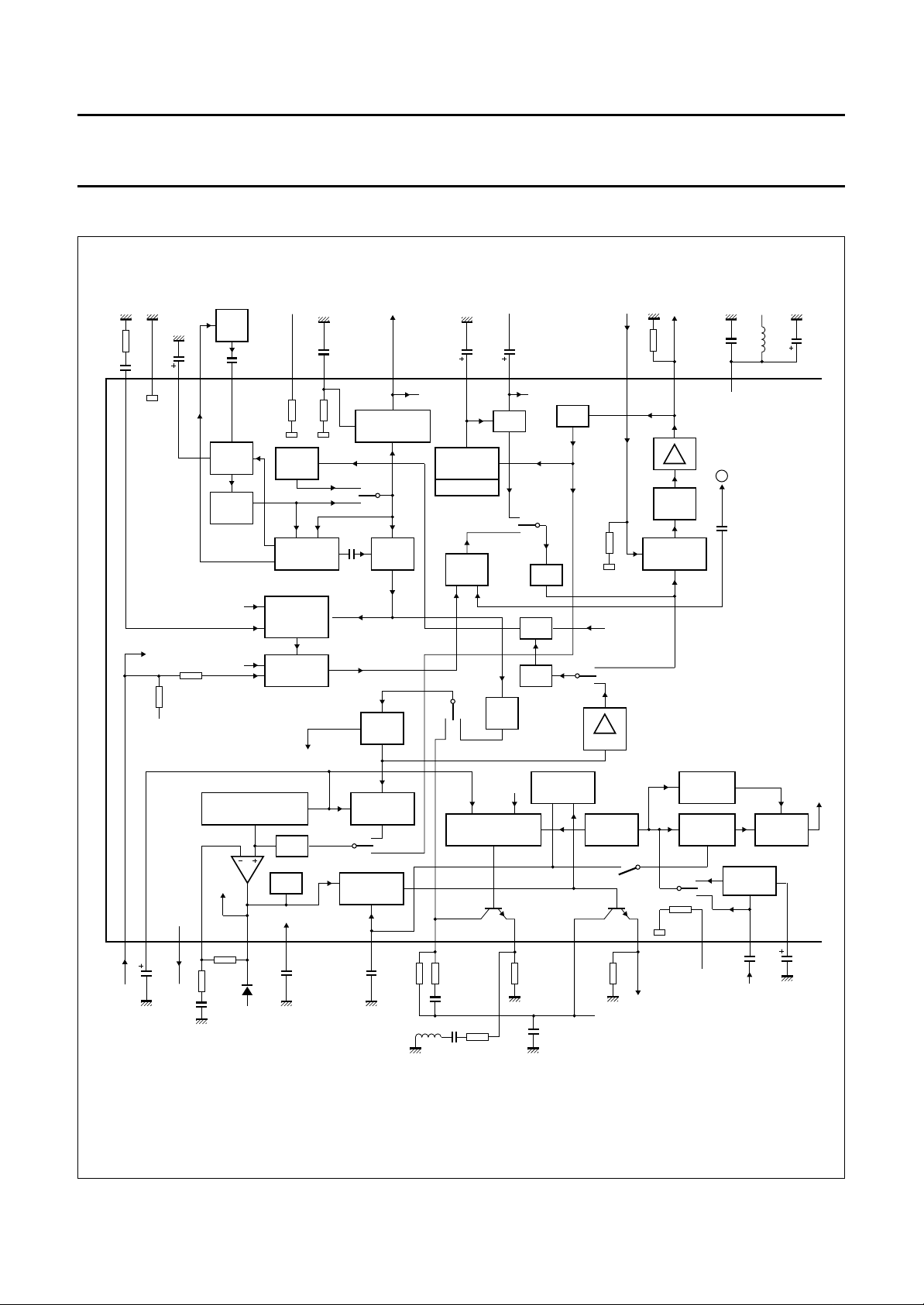
Fig.1 Block diagram (continued in Fig.2).
1996 Oct 14 3
Philips Semiconductors Product specification
Y/C automatic adjustment processor
(VHS standard)
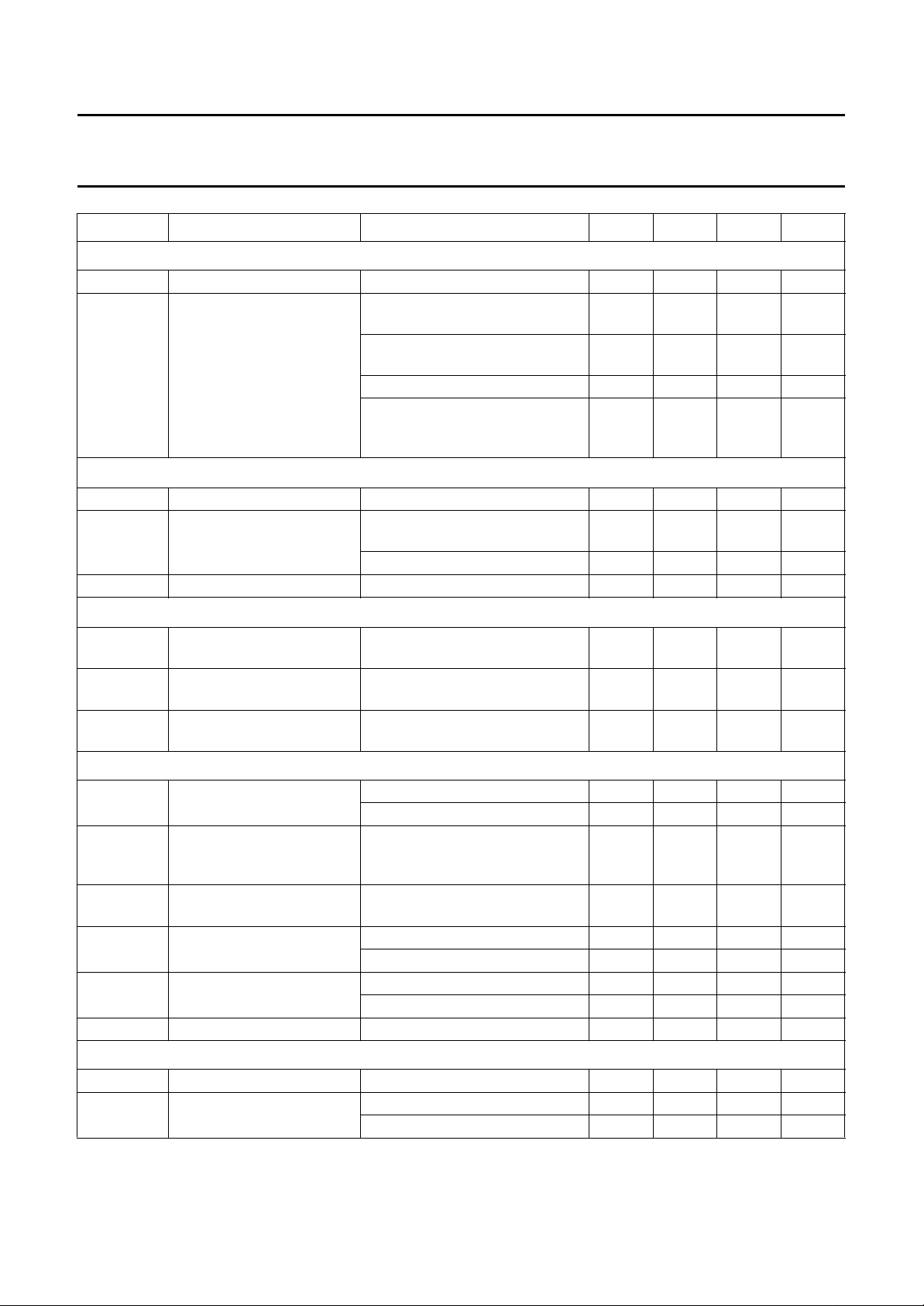
handbook, full pagewidth
CK
H BLANK
AGCKP1
TP1
PBCI
A
PBCO
39 38 37 36 35 34 33 32 31 30 29 28 27
LPF
f
*
C
H/2
NAP
PB/SP
CF892
COMB
-15 dB
4
2
1.3
kΩ
CFI CDO
SEC
10 nF
270 Ω
3
15
µH
COMB
DRIVER
BURST
DOWN
SNP
50 kΩ
from
4 PHI
10 nF
BMI ACCO
BALANCED
MIXER
BURST UP
GND(C)
BPF
630
CFT
PB
REC
V
CC(C)
10 nF
ACC
ACC
DETECTOR
TDA9725
f
CTT
0.1
µF
H/2
REC
DETECTOR
PHI/PB
VXO
RECORD
AFC
FPC
BGP ROT
PB
BPF
4.43
REC
CK/FPC
REC
PB
REC
to BM
4 PHI : 4SLD
120
0.1 µF
(1)
kΩ
470
pF
LFVXO LFVCO
LPF
630
CK
f
sc
DIVIDER
SUBMIXER
LPF
680
Ω
1 µF
(1)
TDA9725
3rd
LOCK
VCO
47
nF
CK
X2
VXO
REC
PB
SEC
MUTE
XTALI XTALO
TEW 8H
f
sc
2 f
4.43619
MHz
sc
f
H/2
4.7 kΩ
V
8.0
kΩ
33
pF
CC(C)
PB
RECPB/LP
from pin 43
MUTE
MUTE
50 kΩ
15 16 17 18 19 20 21 22 23 24 25 26
ELS
CK
HSS
0.1
µF
: 40
(1)
1 µF
TIMER
FCO
FREQUENCY
DETECTOR
22 kΩ
V
MGB695
6.8
µH
CC(C)
(1) Low leakage current.
Fig.2 Block diagram (continued from Fig.1).
1996 Oct 14 4
Philips Semiconductors Product specification
Y/C automatic adjustment processor
(VHS standard)
Table 1 Explanation of symbols in Figs 1 and 2
SYMBOL DESCRIPTION
AGCKP1 mode with shortened key pulse for AGC
BGP burst gate pulse
DOP dropout pulse
f
H
f
sc
HDL CCD charged coupled device with 1H delay
NLDE non-linear de-emphasis
NLEDTE non-linear emphasis/detail enhancer
ROT rotary pulse
VXO voltage controlled XTAL oscillator
YNR vertical noise reduction
YLPF luminance low-pass filter
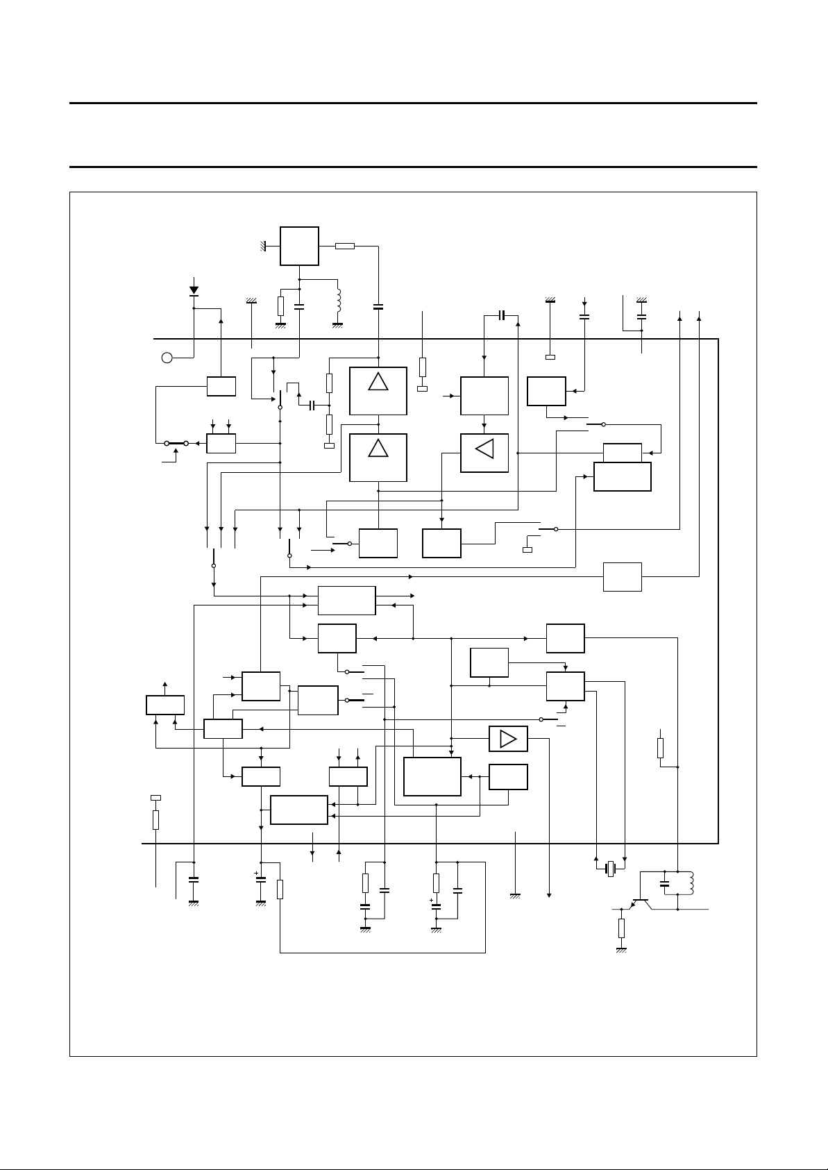
PINNING
SYMBOL PIN DESCRIPTION
PCTL 1 picture control/edit switch input
CDEV 2 deviation/playback AGC detector input
TP2 3 test pin 2/correlation detector output
NFB
MEO
C
CLP3
C
F0E
MDEC 8 main de-emphasis output
MDEB 9 main de-emphasis and peaking output
V
CC(FM)
FMO 11 FM output
PTR 12 switch (PB/TRICK/REC)
FMI 13 playback FM input
C
FMA
ELS
CK 16 colour killer terminal
FCO 17 frequency correction output
BGP 18 burst gate pulse output
line frequency
subcarrier frequency (4.433619 MHz)
negative feedback input of main
4
emphasis
main emphasis output/white
5
clip/modulator input/SQPB selector
6 capacitor for clamp 3
storage capacitor for f0 processor
7
(record)/envelope detector (playback)
10 FM supply voltage
14 storage capacitor for FM AGC
PAL: switch (LP C*/LP/SP); NTSC:
15
switch (EP/LP/SP)
TDA9725
SYMBOL PIN DESCRIPTION
ROT 19 rotary pulse input
LFVXO 20 loop filter VXO
LFVCO 21 loop filter VCO
n.c. 22 not connected; note 1
f
sc
XTALI 24 VXO input from crystal
XTALO 25 VXO output to crystal
2f
sc
f
H/2
CTT 28 chrominance output to tape
V
CC(C)
CFT 30 playback chrominance input from tape
GND(C) 31 chrominance ground
ACCO 32 automatic chrominance control output
BMI 33 balanced mixer input
SNP 34 switch (SECAM/NTSC/PAL)
CDO 35 comb driver output
CFI 36 chrominance input from comb filter
TP1 37 test pin 1; note 1
PBCO 38 playback chrominance output
PBCI 39 playback chrominance input
V
CC(Y)
CVBSO 41 CVBS output
CHI 42 character insertion input (artificial
CVBSI 43 CVBS input
C
AGC
SYNC 45 sync separator push-pull output
C
SS
YNR 47 YNR switch
VFC 48 video input from 1HDL CCD
VTC 49 video output to 1HDL CCD
C
CCD
GND(Y) 51 luminance ground
LPNC 52 low-pass filter noise canceller
Note
1. It is recommended that this pin should be connected to
ground.
23 fsc output
26 2fsc output
27 f
H/2
output
29 chrominance supply voltage
40 luminance supply voltage
sync/black/white/through)
44 AGC detector capacitor
46 sync separator detector capacitor
50 storage capacitor for CCD AGC level
1996 Oct 14 5
Philips Semiconductors Product specification
Y/C automatic adjustment processor
(VHS standard)
handbook, halfpage
PCTL
CDEV
C
CLP3
C
MDEC
MDEB
V
CC(FM)
C
LFVXO
LFVCO
XTALI
XTALO
TP2
NFB
MEO
F0E
FMO
PTR
FMI
FMA
ELS
CK
FCO
BGP
ROT
n.c.
f
2f
1
2
3
4
5
6
7
8
9
10
11
12
13
TDA9725
14
15
16
17
18
19
20
21
22
23
sc
24
25
26
sc
MGB693
52
51
50
49
48
47
46
45
44
43
42
41
40
39
38
37
36
35
34
33
32
31
30
29
28
27
LPNC
GND(Y)
C
CCD
VTC
VFC
YNR
C
SS
SYNC
C
AGC
CVBSI
CHI
CVBSO
V
CC(Y)
PBCI
PBCO
TP1
CFI
CDO
SNP
BMI
ACCO
GND(C)
CFT
V
CC(C)
CTT
f
H/2
TDA9725
Fig.3 Pin configuration.
1996 Oct 14 6
Philips Semiconductors Product specification
Y/C automatic adjustment processor
(VHS standard)
FUNCTIONAL DESCRIPTION
Record (REC)/electric to electric (EE) mode
UMINANCE
L
From input pin 43 the CVBS signal is fed via the automatic
gain control (AGC) and subclamp (SCL) to the output
pin 41. Instead of the controlled and clamped CVBS signal
it is also possible to switch (dependent on the level at
pin 42) white, black or sync-level to this pin. To eliminate
chrominance parts the CVBS signal is fed to the luminance
low-pass filter (YLPF) and to the sync separator stage.
The sync signal is available at pin 45. The signal is also fed
via vertical emphasis non-linear emphasis (NLE),
deviation control stage, main emphasis and white-dark clip
to the FM modulator. The FM signal is available at pin 11.
HROMINANCE
C
The chrominance signal is selected out of CVBS (from
pin 43) in BPF 4.43 MHz (band-pass filter) and controlled
in automatic chrominance control (ACC).
The chrominance signal is mixed with 5.06 MHz to
627 kHz and via LPF 627 kHz to the output pin 30.
TDA9725
Playback (PB)/video to video (VV) mode
LUMINANCE
The FM signal is fed via FM AGC and double limiter to the
controlled FM demodulator. After demodulation and
filtering in sub low-pass filter (SUBLPF) main
de-emphasis, YLPF and non-linear de-emphasis the
signal is fed to the vertical noise reduction (YNR) and in
parallel to the sync separator. The chrominance signal is
added in the Y/C mixer. The complete CVBS signal is
available at pin 41.
HROMINANCE
C
The 627 kHz chrominance signal coming from tape via
BPF 627 kHz and field ACC to the balanced mixer. Mixed
with 5.06 MHz the 4.43 MHz chrominance signal is fed via
comb driver stage to the external comb filter (pin 35) and
via internal conjugated complex (C*) stage and internal AC
coupling to the luminance part.
Record and playback
In both modes record (REC) and playback (PB) the
5.06 MHz mixer frequency is produced by the 20.24 MHz
voltage controlled oscillator (VCO) and a divide-by-four.
LIMITING VALUES
In accordance with the Absolute Maximum Rating System (IEC 134).
SYMBOL PARAMETER CONDITIONS MIN. TYP. MAX. UNIT
V
V
V
I
P
T
T
V
CC
I
n
I
tot
stg
amb
es
supply voltage 0 − 6.0 V
input voltage at pin 22 0 − 1.6 V
input voltage on all other pins 0 − V
CC
input current at pin 22 −−10 mA
total power dissipation −−1250 mW
storage temperature −25 − +150 °C
operating ambient temperature −20 − +70 °C
electrostatic handling for all pins note 1 −300 − +300 V
Note
1. Charge device model class B: discharging a 200 pF capacitor via a 0 Ω series resistor.
THERMAL CHARACTERISTICS
SYMBOL PARAMETER VALUE UNIT
R
th j-a
thermal resistance from junction to ambient in free air 43 K/W
V
1996 Oct 14 7
Philips Semiconductors Product specification
Y/C automatic adjustment processor
TDA9725
(VHS standard)
CHARACTERISTICS
VCC=5V; T
Luminance part: All amplitudes are VBS peak-to-peak values, unless otherwise specified.
Chrominance part: All amplitudes for P AL and NTSC are red values with 75% saturation and chrominance-to-burst ratio
of 2.2 : 1, unless otherwise specified.
SYMBOL PARAMETER CONDITIONS MIN. TYP. MAX. UNIT
Supplies
V
CC
I
PB
I
REC
FM SUPPLY (PIN 10)
I
PB
I
REC
CHROMINANCE SUPPLY (PIN 29)
I
CC(C)
UMINANCE SUPPLY (PIN 40)
L
I
PB
I
REC
Picture control/edit switch input (pin 1)
V
1
= +25 °C and typical application (see Figs 1 and 2), unless otherwise specified.
amb
supply voltage 4.5 5.0 5.5 V
current consumption
playback mode 140 170 200 mA
(I10+I29+I40)
current consumption
record mode 125 155 185 mA
(I10+I29+I40)
DC playback current − 22 − mA
DC record current − 12 − mA
DC supply current playback mode − 85 − mA
record mode − 85 − mA
DC playback current − 63 − mA
DC record current − 57 − mA
DC input voltage pin open-circuit − 1.6 − V
sharp picture 0 − 1.6 V
soft picture 1.6 − 3.2 V
edit mode 4.1 − 5.0 V
Deviation/playback AGC detector input (pin 2)
V
2
detection voltage 1.8 2.5 3.2 V
Test pin 2/correlation detector output (pin 3)
V
OH
HIGH level output voltage correlation of Y signal;
pin 37 LOW; RL≥ 10 kΩ
V
OL
LOW level output voltage non-correlation of Y signal − 0.1 0.5 V
1996 Oct 14 8
1.5 2.1 3.0 V
Philips Semiconductors Product specification
Y/C automatic adjustment processor
TDA9725
(VHS standard)
SYMBOL PARAMETER CONDITIONS MIN. TYP . MAX. UNIT
Negative feedback input of main emphasis (pin 4; open-base) and main emphasis
output/white-clip/modulator/SQPB selector (pin 5)
F
EEDBACK LOOP CLOSED (PIN 4 CONNECTED TO PIN 5; MAIN EMPHASIS OFF)
V
SY
V
oREC(p-p)
t
FRAMEDET
NON-LINEAR EMPHASIS/DETAIL ENHANCER; notes 2 and 3
RD1 response D1 −20 dB; f
RD2 response D2 −20 dB; f
RS1 response S1 −20 dB; f
RS1 response S2 −20 dB; f
RL1 response L1 −20 dB; f
RL2 response L2 −20 dB; f
RL3 response L3 0 dB; f
VERTICAL EMPHASIS
PL1 peak level 1 −30 dB recursive; note 4 3.5 4.3 5.3 dB
PL2 peak level 2 −20 dB recursive; note 4 3.5 4.0 4.5 dB
PL3 peak level 3 0 dB recursive 0 0.4 1.0 dB
EEDBACK LOOP NORMAL APPLICATION
F
DCL dark-clip level 50 60 70 %
WCL white-clip level 180 187 194 %
V
5
Record storage capacitor for f
V
I
V
NOR
V
OFF
V
NS
G
Eon
t
env
DC voltage level sync tip − 1.9 − V
record output voltage level;
standard output level
(peak-to-peak value)
time for correcting carrier
video/sync = 7/3;
450 500 550 mV
∆VCC= ±0.25 V;
T
= −10 to +70 °C
amb
HIGH during half picture 1; note 1 −−200 ms
interleave relationship to
half picture
= 500 kHz; SP; NORM 1.7 2.7 3.7 dB
i
= 2 MHz; SP; NORM 6.0 7.5 9.0 dB
i
= 500 kHz; SP; EDIT 1.0 1.7 2.4 dB
i
= 2 MHz; SP; EDIT 4.5 5.5 6.5 dB
i
= 500 kHz; LP 3.1 4.4 5.7 dB
i
= 2 MHz; LP 7.0 9.0 11 dB
i
= 2 MHz; LP 1.6 2.3 3.0 dB
i
SQPB input voltage playback mode 4.0 −−V
processor and playback storage capacitor for envelope detector (pin 7)
0
DC voltage record mode − 1.2 − V
DC voltage of normal mode playback mode;
= 350 mV (p-p); pin 14 HIGH
V
i
DC voltage of dropout
playback mode 0 − 1.3 V
2.3 3.3 4.0 V
correction (DOC) off mode
DC voltage at no input
playback mode 1.1 1.6 2.1 V
signal
envelope detector
switch-on level
(dropout active)
envelope detector operating
playback mode;
−13 −10 −7dB
0dB=Vi= 350 mV (p-p);
fi= 3.8 MHz; pin 14 HIGH
Ci= 0.1 µF 380 500 620 µs
time
1996 Oct 14 9
Philips Semiconductors Product specification
Y/C automatic adjustment processor
TDA9725
(VHS standard)
SYMBOL PARAMETER CONDITIONS MIN. TYP. MAX. UNIT
Main de-emphasis output (pin 8; open collector)
V
8
V
VID(p-p)
Φ
DEM
LIN1 demodulator linearity 1 VHS mode 0.97 1.0 1.03
LIN2 demodulator linearity 2 SQPB mode 0.90 1.0 1.07
Main de-emphasis and peaking output (pin 9)
V
9
V
VR(p-p)
α
DEM
DC output voltage fi= 3.8 MHz at VHS 2.9 3.4 3.9 V
video output voltage level
f
= 1 MHz 230 300 370 mV
DEV
(peak-to-peak value)
demodulator sensitivity VHS mode 0.23 0.3 0.37 V/MHz
SQPB mode 0.14 0.19 0.24 V/MHz
V05 MHz()V
-------------------------------------------------------------------V
4 MHz()V
0
9 MHz()V
V
0
-------------------------------------------------------------------V
7 MHz()V
0
4MHz()–
0
3MHz()–
0
7MHz()–
0
5MHz()–
0
DC output voltage fi= 3.8 MHz at VHS 1.1 1.6 2.1 V
reverse video voltage level
230 300 370 mV
(peak-to-peak value)
suppression of
40 −−dB
demodulated carrier
FM output (pin 11)
V
11
DC mean value output
voltage
V
11(p-p)
output voltage level
(peak-to-peak value)
f
sync
∆f
sync
sync output frequency V5=V
stability of sync output
frequency
f
∆f
dev
dev
frequency deviation V5=V
stability of frequency
deviation
∆f
H
L
rot
2
mod
carrier interleave frequency rotary pulse (pin 19) HIGH/LOW;
second harmonic distortion fi= 3.8 MHz −−50 −42 dB
modulator linearity 0.95 1.00 1.05
RL=1kΩ 2.9 3.2 3.5 V
RL=1kΩ 0.7 0.9 1.1 V
; V43= 0 dB 3.75 3.8 3.85 MHz
sync
∆VCC= ±0.25 V
or T
= −10 to +70 °C
amb
; V43= 0 dB;
white
−20 − +20 kHz
0.95 1.0 1.05 MHz
video/sync = 7/3
∆VCC= ±0.25 V
or T
= −10 to +70 °C
amb
−20 − +20 kHz
6.8 7.8 8.8 kHz
at SP and LP
1996 Oct 14 10
Philips Semiconductors Product specification
Y/C automatic adjustment processor
TDA9725
(VHS standard)
SYMBOL PARAMETER CONDITIONS MIN. TYP. MAX. UNIT
Switch: PB/TRICK/REC (pin 12)
R
I
internal resistance to
ground
V
PB
voltage range for active
playback mode
V
TR
voltage range for active
trick mode
V
REC
voltage range for active
record mode
Playback FM input (pin 13)
V
V
13
i(p-p)
DC voltage 1.7 2.2 2.7 V
input voltage level
(peak-to-peak value)
V
iBO(p-p)
boundary input voltage
(peak-to-peak value)
G
DOC
∆G
hys
G
Eon
DOC on level Vi= 350 mV (p-p); fi= 3.8 MHz;
DOC on/off hysteresis Vi= 350 mV (p-p); fi= 3.8 MHz;
envelope detector
switch-on level
FM AGC active 63 200 632 mV
FM AGC not active; pin 14 HIGH − 350 − mV
fi= 3.8 MHz; pin 14 HIGH 10 − 1000 mV
pins 7 and 14 HIGH
pins 7 and 14 HIGH
playback mode;
0dB=Vi= 350 mV (p-p);
fi= 3.8 MHz; pin 14 HIGH
40 50 60 kΩ
3.5 − 5V
1.75 − 3V
0 − 1.25 V
−18 −15 −12 dB
135dB
−13 −10 −7dB
Storage capacitor for FM AGC (pin 14; playback mode)
V
14
DC voltage AGC on 2.6 3.1 3.6 V
DC input voltage AGC off 4.3 − 5.0 V
Switch LP C*/LP/SP at PAL; EP/LP/SP at NTSC (pin 15)
R
I
internal resistance to
ground
V
C
input voltage for active C*
PAL 3.5 − 5V
(conjugated complex
chrominance signal)
V
E
V
L
V
S
input voltage for active EP NTSC 3.5 − 5V
input voltage for active LP 1.75 − 3V
input voltage for active SP 0 − 1.25 V
40 50 60 kΩ
1996 Oct 14 11
Philips Semiconductors Product specification
Y/C automatic adjustment processor
TDA9725
(VHS standard)
SYMBOL PARAMETER CONDITIONS MIN. TYP. MAX. UNIT
Colour killer terminal (pin 16)
V
V
V
CK
CK
NC
16
th
th
hys
DC voltage black and white luminance input without
input voltage forced colour off 0 − 1.5 V
threshold voltage colour on 2.0 2.2 2.4 V
colour killer threshold relative to nominal input;
colour killer hysteresis relative to nominal input;
Frequency correction output (pin 17)
V
17
I
oSLD
t
SLD
f
SLH
operating range 0.8 − 4.2 V
SLD output current SLD ±12 ±17 ±22 µA
SLD pulse duration SLD − 1 − t
start of detection at positive
frequency deviation
(referenced to fsc+N×fH at
pin 35; −I17)
f
SLL
start of detection at
negative frequency
deviation (referenced to
fsc+N×fH at pin 35; +I17)
I
ofDET
output current of frequency
detector
t
fDET
frequency detector pulse
duration
f
fDETH
start of detection at positive
frequency deviation
(referenced to fsc+N×fH at
pin 35; −I17)
f
fDETL
start of detection at
negative frequency
deviation (referenced to
fsc+N×fH at pin 35; +I17)
chrominance
forced colour on 3.0 − 4.3 V
V30= 110 mV (p-p)
V30= 110 mV (p-p)
SLD/PAL 1.0 2.0 3.0 kHz
SLD/NTSC 2.0 4.0 5.0 kHz
SLD/PAL −3.0 −2.0 −1.0 kHz
SLD/NTSC −5.0 −4.0 −2.0 kHz
FDET ±12 ±17 ±22 µA
FDET 68 73 78 µs
record mode 40 70 100 kHz
record mode −100 −70 −40 kHz
1.6 1.8 2.0 V
−25 −30 −35 dB
135dB
H
1996 Oct 14 12
Philips Semiconductors Product specification
Y/C automatic adjustment processor
TDA9725
(VHS standard)
SYMBOL PARAMETER CONDITIONS MIN. TYP. MAX. UNIT
Burst gate pulse output (or sandcastle output; pin 18); note 5
t
BGP
t
BGS
V
O(L)
V
O(M)
V
O(H)
t
VBL(start)
t
VBL(stop)
Rotary pulse input (pin 19; open PNP base)
V
C2
V
C1
burst gate pulse duration 4.2 4.45 4.7 µs
start of burst gate beyond
3.25 3.5 3.75 µs
sync start at pin 45
LOW level DC output
voltage
medium level DC output
voltage
HIGH level DC output
voltage
vertical blanking of BGP
start
vertical blanking of BGP
stop
inactive; I18=1mA −−0.7 V
inactive; I
horizontal blanking;
10 kΩ connected to V
=0mA −−0.5 V
18
2.2 2.6 3.0 V
CC
BGP; I18= −0.4 mA 4.0 4.4 − V
BGP; I
referring to first equalisation
=0mA 4.6 −−V
18
− 0 − t
pulse in mid of line
referring to rotary transition 23 −−t
referring to last equalisation pulse
1 −−t
in mid of line
voltage for −90° phase
channel 2 0 − 2.25 V
rotation
voltage for non-rotation
channel 1 2.75 − 5V
(PAL) or +90° rotation
(NTSC)
H
H
H
Loop filter VXO (pin 20; record mode)
V
Φ
f
PI(U)
f
PI(L)
20
VXO
DC voltage 1 2.4 3.6 V
VXO sensitivity −1.6 −1.2 −0.8 Hz/mV
upper pull-in frequency 0.6 1.0 1.8 kHz
lower pull-in frequency −1.8 −1.0 −0.6 kHz
Loop filter VCO (pin 21)
V
21
Φ
VCO
output (pin 23)
f
sc
V
23
V
o(p-p)
DC voltage 1.3 2.1 2.9 V
VCO sensitivity fH related; record mode −34 −38 −42 kHz/V
DC output voltage 1.8 2.3 2.8 V
output signal voltage
(peak-to-peak value)
H
2
H
3
second harmonic distortion −−−25 dB
third harmonic distortion −−−20 dB
VXO input from crystal (pin 24); note 6
V
24
DC voltage 2.6 3.0 3.4 V
f
related; playback mode −1.3 −1.5 −1.7 MHz/V
sc
no load 500 600 700 mV
1996 Oct 14 13
Philips Semiconductors Product specification
Y/C automatic adjustment processor
TDA9725
(VHS standard)
SYMBOL PARAMETER CONDITIONS MIN. TYP. MAX. UNIT
VXO output to crystal (pin 25)
V
25
∆f
osc
2f
output (pin 26)
sc
V
26
V
o
H
2
output; coupled to burst sequence (pin 27)
f
H/2
V
O(L)
V
O(H)
V
NTSC4.43
DC output voltage 2.9 3.3 3.7 V
deviation of oscillator
frequency
due to internal spread;
playback mode
video signal without burst;
−50 − +50 Hz
−1.4 − +1.4 kHz
record mode
no video signal; record mode −100 − +100 Hz
= 4.75 to 5.25 V;
V
CC
= −10 to +70 °C;
T
amb
−100 − +100 Hz
playback mode
DC output voltage 4.5 4.9 − V
output signal voltage 1.2 kΩ connected to VCC and
40 55 70 mV
emitter follower (EF)
tuned LC circuit to V
and EF 400 550 700 mV
CC
second harmonic distortion tuned LC circuit (Q > 20) and EF −−−30 dB
LOW level DC output
burst phase = +135°−−0.5 V
voltage
HIGH level DC output
burst phase = −135° 4.5 −−V
voltage
input level for forced
NTSC; playback mode −−1.5 V
NTSC 4.43 mode (no NAP)
Chrominance output to tape (pin 28); see Table 2
V
28
DC output voltage colour on 2.1 2.4 2.7 V
colour killer active − 0.1 0.3 V
V
o(p-p)
chrominance output signal
record mode; PAL 467 660 932 mV
voltage (N × fH)
(peak-to-peak value)
G
UP
SECAM-fOR burst related
SECAM 0.2 1.0 1.8 dB
to PAL burst
H
2
H
3
α
CK
second harmonic distortion V33=0dB −−−40 dB
=+6dB −−−35 dB
V
33
third harmonic distortion V33=0dB −−−40 dB
=+6dB −−−35 dB
V
33
colour killer suppression 40 −−dB
Playback chrominance input from tape (pin 30)
V
V
30
i(p-p)
DC voltage 1.7 2.2 2.7 V
input signal voltage
(peak-to-peak value)
chrominance + FM −−310 mV
chrominance 11 110 220 mV
1996 Oct 14 14
 Loading...