

Philips tda9715h DATASHEETS

INTEGRATED CIRCUITS
DATA SH EET
TDA9715H/A
Y/C one-chip processor
(VHS standard)
Product specification
Supersedes data of August 1993
File under Integrated Circuits, IC02
1996 Oct 21
Philips Semiconductors Product specification
Y/C one-chip processor (VHS standard) TDA9715H/A
FEATURES
• Luminance Noise Reduction (YNR)
• Chrominance Noise Reduction (CNR)
• Saturation dependent writing current control (CACC)
GENERAL DESCRIPTION
The TDA9715H/A is an integrated circuit for chrominance
and luminance processing (record and playback) in VHS
tape recorders for the TV standard PAL, NTSC,
SECAM/ME (4.43 MHz chrominance systems).
• Integrated filter
• Simple SVHS playback
• Skew output for long-play TRICK mode.
QUICK REFERENCE DATA
SYMBOL PARAMETER CONDITIONS MIN. MAX. UNIT
V
CC
I
CC
T
amb
T
stg
supply voltage 4.5 5.5 V
supply current VCC=5V − 200 mA
operating ambient temperature −20 +70 °C
storage temperature −25 +150 °C
ORDERING INFORMATION
TYPE
NUMBER
NAME DESCRIPTION VERSION
PACKAGE
TDA9715H/A QFP80 plastic quad flat package; 80 leads (lead length 1.6 mm);
body 14 × 20 × 3.0 mm
SOT310-1
1996 Oct 21 2
Philips Semiconductors Product specification
Y/C one-chip processor (VHS standard) TDA9715H/A
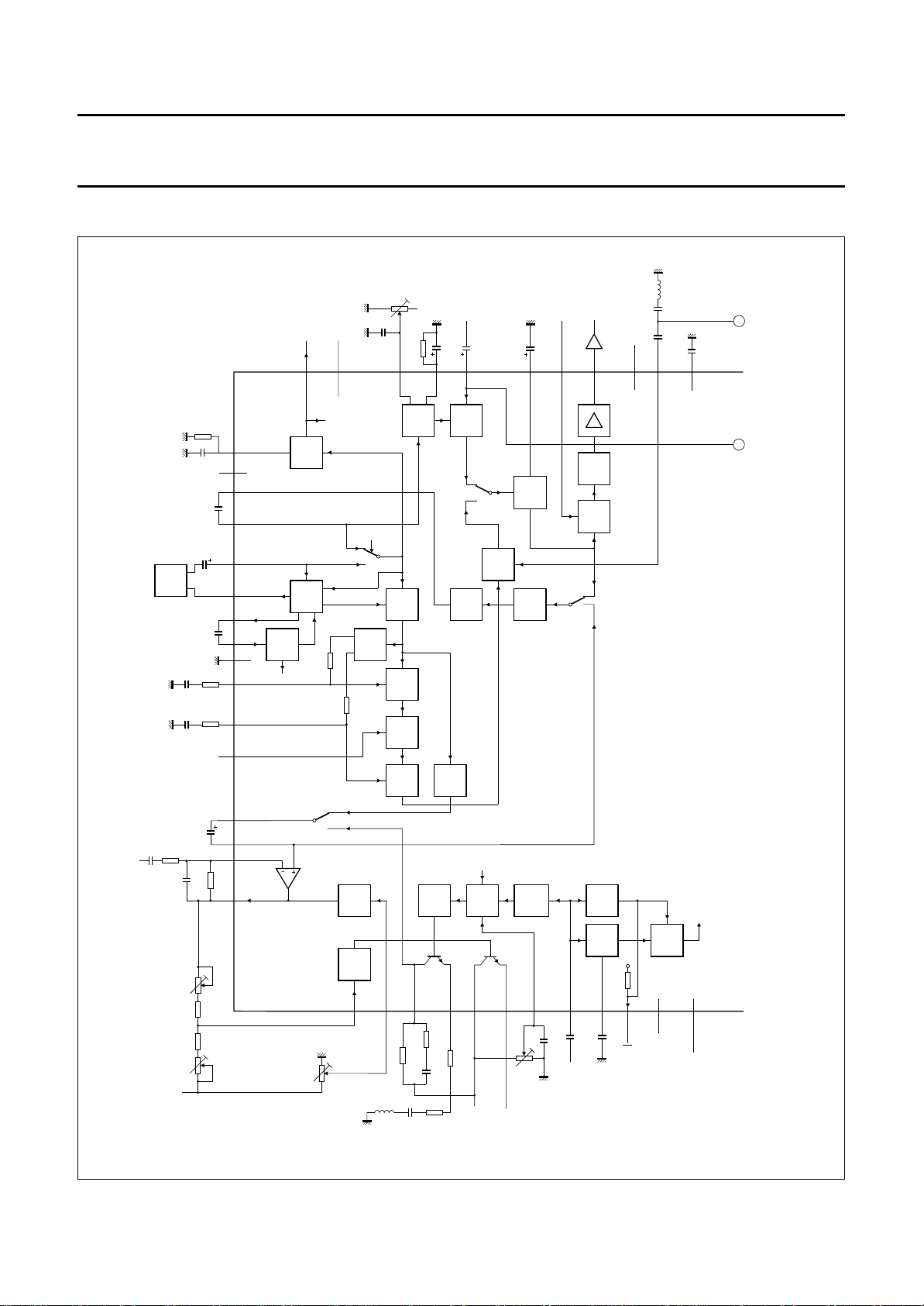
BLOCK DIAGRAM
handbook, full pagewidth
EDIT/YNR OFF/NORM
H/M/L
1HDL
CCD
220 Ω
1 nF
5 pF
4.7 kΩ
DEV
2.7 kΩ
4.7 kΩ
V
CC
47 pF
390 pF
10 kΩ
FO
220 kΩ
22 nF
33 nF
1 µF
10 µF
510 Ω
510 Ω
PICT.CTL
10
µF
400
1 kΩ
EE level
22 kΩ
SQPB
HSS OUT
64
HSS
65
66
67
68
69
70
71
72
73
74
75
76
77
78
79
80
CORR
ME
CORR
SYNC
SEP
YNR
PROC
22 kΩ
REC
PB
W/DC
MOD
1
WHITE CLIP
HPLIM
10 nF
DOP
120 µH
YNR
MIX
NC1
PICT
NC2
2
peaking
6263
56 pF
1.2
MΩ
1.5
kΩ
VIDEO
V
CC
IN
4.7
10
µF
µF
6061
DET
AGC
EE
VV
NLDE
EE:OFF
NLE
DTE
SQPB
DLPF
MDE
3456789101112
3.3 kΩ
FM
DEM
Y
470
680
pF
39
pF
VCC2
Ω
1.5
kΩ
+
V
CC
Y/C
MIX
RECFMY
SCL
Y
LPF
DOUBLE
LIM
22 kΩ
PB
level
3.3
µF
mF
10
AVP
PBRFY
10
mF
VIDEO
OUT
NOISE
CLIP
H/V
INSERT
EE
VV
DET
ENV
DET
575859
DO
22
mF
µH
V
CC
55
56
Y
VCC1
TDA9715H/A
GATE
EE/VV/TRICK
H/M/L
DO
27
27
pF
10 nF
54
DOP
SP/LP/EP
L/M/H
MHA428
1
10 nF
2
1996 Oct 21 3
Fig.1 Block diagram (continued in Fig.2).

Philips Semiconductors Product specification
Y/C one-chip processor (VHS standard) TDA9715H/A
0.1 µF
COMB
−15 dB
10
15
nF
µH
50
EE
TDA9715H/A
PHI
F-DET
L/M/H
SC
270 Ω
CK
FPC
DET
VXO
SEC
PB
1.2
kΩ
VV
EE
4 PHI ÷4
ROT
C/BW/NOR
10
nF
REC
AFC
MUTE
DET
H/M/L
820
Ω
180
Ω
COMB
DRIVER
DOWN
EE
VV
to BMFPC
0.1
µF
BU
BPF
4.43
MUTE
4849
VV
EE
120
kΩ
0.1
µF
TEST1 TEST2
LPF
630
DET
46
470
pF
BM
BU UP
DIVIDER
SUBMIXER
LPF
45
0.1
µF
SEC
MUTE
47
4PHI
f
0.1
µF
fr.
CACC
CACC
sc
44
BPF
630
ACC
ACC
DET
CKN
× 2
VXO
EE
VV
1.2
10
kΩ
nF
1
µF
CNR TP
CNR TP
CNR off
VV
VCO
CHR
f.TAPE
10 nF
414243
40
V
Chr.
CC
EE
270 Ω
(±1%)
V
CC
39
0.15 µF
0.15 µF
47 µF
33 pF + 2.7 pF
0.01 µF
VSXO162
V
6.8 µH
10 kΩ
f
sc
CC
10 nF
18 nF
22
kΩ
CHR. TO TAPE
V
CC
10
pF
V
CC
2f
sc
500
4.7
kΩ
120 µH
1 nF
2.2 kΩ
38
37
36
35
34
33
32
31
30
29
28
27
26
25
MHA429
handbook, full pagewidth
1
2
0.1
µF
NT/PAL/SE
L/M/H
pin 42
CNR
f
H
52
VV/SP
2 H
DELAY
EE
10
nF
51
VV
HSS
CKN
1
kΩ
820
Ω
53
VV/LP
TIMER
÷40
SKEW
SLD
DET
13 14 15 16 17 18 19 20 21 22 23 24
SLDCK
SKEW
REC/PB/ID
1
22
µF
kΩ
1996 Oct 21 4
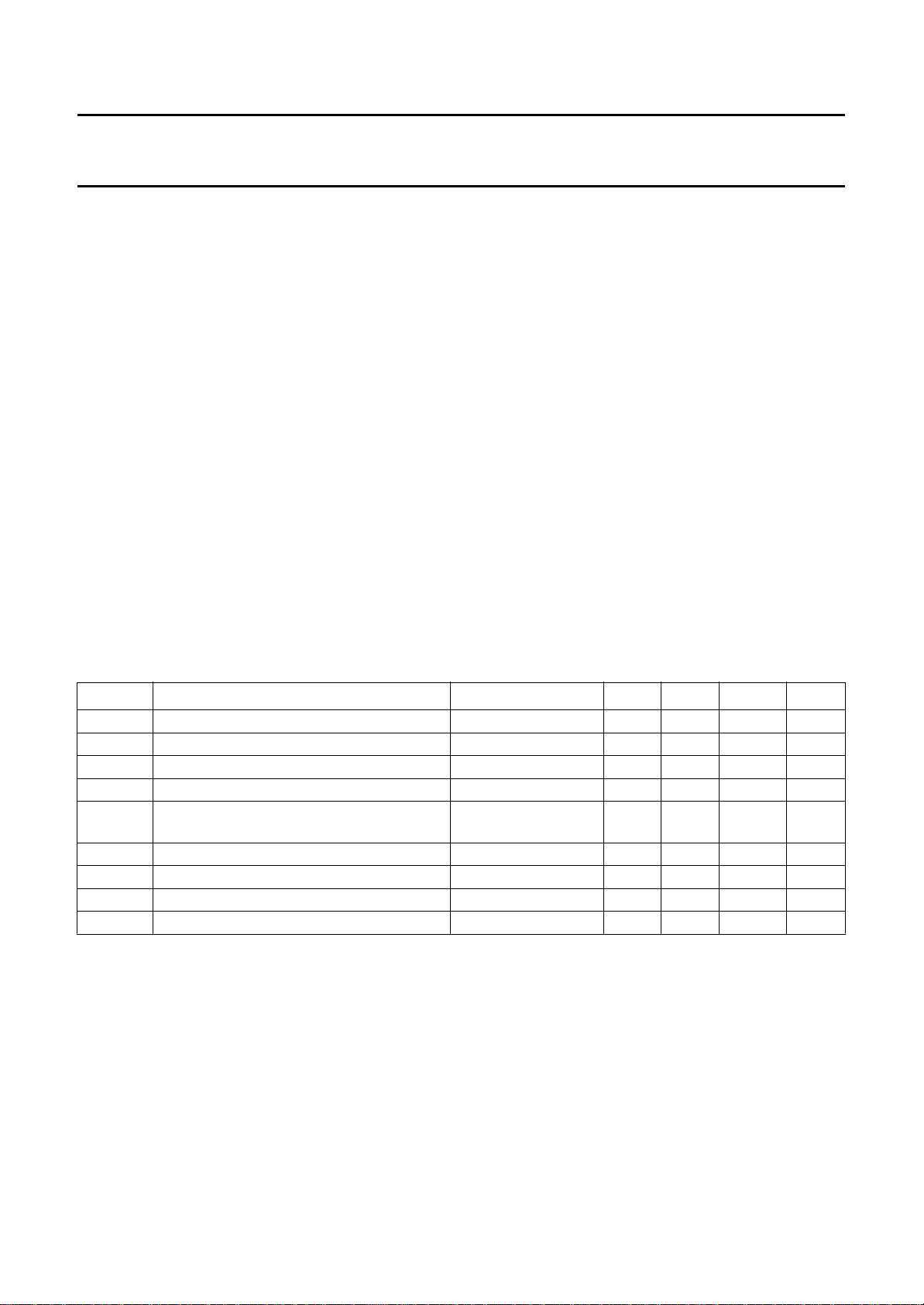
Fig.2 Block diagram (continued from Fig.1).
Philips Semiconductors Product specification
Y/C one-chip processor (VHS standard) TDA9715H/A
FUNCTIONAL DESCRIPTION
Record/Electric-to-Electric (REC/EE) mode
UMINANCE
L
The CVBS signal appears at the output pin 57 and at the
internal Y Low-Pass Filter (YLPF) via pin 60 and
Automatic Gain Control (AGC) stage. Exempt from
chrominance, the luminance signal is fed first to the sync
separator stage to obtain the separated sync pulse at
pin 64 and secondly via Non-Linear Emphasis (NLE), main
emphasis, white-dark clip and FM modulator to the FM
output pin 6.
HROMINANCE
C
Exempt from the luminance signal in the internal 4.43 MHz
band-pass filter and controlled by the Automatic
Chrominance Control (ACC) stage the chrominance signal
is mixed in the band mixer with a 4-phase shifted 5.06 MHz
signal, produced by the internal adjustment-free oscillator.
The formed N × fH signal is fed via an internal low-pass
Playback/Video-to-Video (PB/VV) mode
LUMINANCE
The FM signal is fed to the FM demodulator stage and the
internal sub low-pass filter (DLPF) via input pin 8 and the
double limiter. After passing main de-emphasis,
Non-Linear De-emphasis (NLDE) and the luminance
Noise Reduction (YNR) the signal is fed first to the sync
separator stage and then (via picture control stage) mixed
with the chrominance signal. This CVBS signal is output at
pin 57.
HROMINANCE
C
The internal N × fH band-pass filter (BPF 627 kHz) and the
ACC stage the signal is mixed in the band mixer with a
4-phase shifted 5.06 MHz signal, produced by the internal
adjustment-free oscillator via input pin 41. The formed
fSC-chrominance signal is fed via internal BPF 4.43 MHz,
external comb filter and internal Chrominance Noise
Reduction (CNR) to the internal Y/C mixer.
filter and CACC to the output at pin 34.
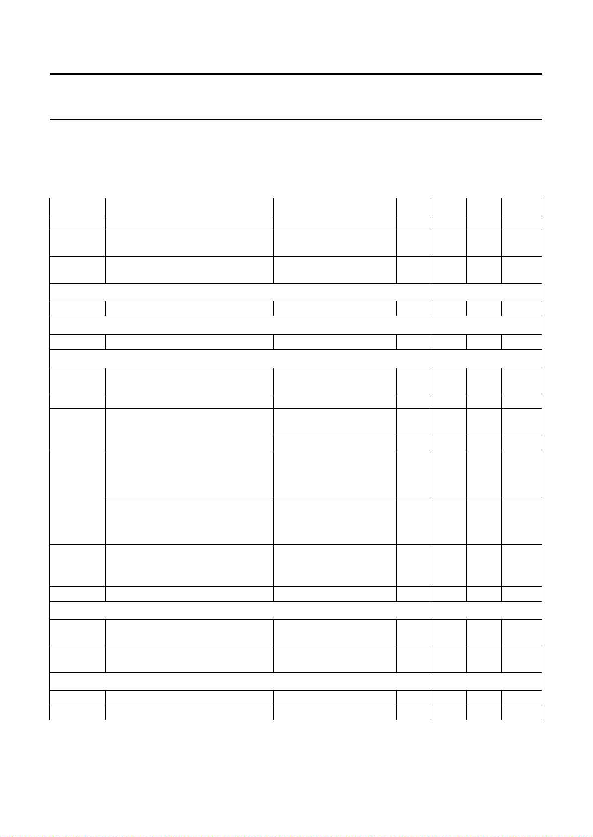
LIMITING VALUES
In accordance with the Absolute Maximum Rating System (IEC 134).
SYMBOL PARAMETER CONDITIONS MIN. TYP. MAX. UNIT
V
CC
V
65
V
I
V
n
I
O
P
tot
T
stg
T
amb
V
es
supply voltage −−5.5 V
voltage V
input voltage V68, V69, V
65
78
input voltage on all other pins 0 − V
output currents −I4, −I6, +I24, −I39, −I57, −I67,
−I71, −I77, −I
80
referenced to GND −−4.5 V
referenced to GND −−4.1 V
CC
−−10 mA
V
total power dissipation see Fig.3 − 1887 − mW
storage temperature −25 − +150 °C
operating ambient temperature see Fig.3 −20 − +70 °C
electrostatic handling for all pins note 1 −300 − +300 V
Note
1. Charge device model class B: equivalent to discharging a 200 pF capacitor via a 0 Ω series resistor.
QUALITY SPECIFICATION
In accordance with
“URV-4-2-59/601”
.
1996 Oct 21 5
Philips Semiconductors Product specification
Y/C one-chip processor (VHS standard) TDA9715H/A
CHARACTERISTICS
VCC=5V; T
Luminance part: All amplitudes are VBS peak-to-peak values, unless otherwise specified.
Chrominance part: All amplitudes for P AL and NTSC are red values with 75% saturation and chrominance-to-burst ratio
of 2.2 : 1, unless otherwise specified.
SYMBOL PARAMETER CONDITIONS MIN. TYP. MAX. UNIT
V
CC
I
P
I
R
Modulator input (pin 1)
ϕ sensitivity 10 12.5 15 kHz/µA
White clip control (pin 2; open base)
CTLϕ control sensitivity 60 80 100 %/V
= +25 °C and typical application (see Figs 1 and 2), unless otherwise specified.
amb
supply voltage 4.5 4.95 5.5 V
current consumption
140 165 200 mA
(I5+I25+I29+I40+I56) at PB/VV
current consumption
130 150 180 mA
(I5+I25+I29+I40+I56) at REC/EE
Main de-emphasis output (pin 3; open collector)
V
3
DC voltage FM input = 3.8 MHz;
V7= 1.7 V
V
s3(p-p)
video signal (peak-to-peak value) V7= 1.7 V 230 300 370 mV
DEMϕ demodulator sensitivity normal VHS mode;
= 1.7 V
V
7
SQPB mode 0.14 0.19 0.24 V/MHz
LIN
α
f
b
3
demodulator linearity
V05 MHz()V
-------------------------------------------------------------------4 MHz()V
V
0
4 MHz()–
0
3 MHz()–
0
demodulator linearity
9 MHz()V
V
0
-------------------------------------------------------------------7 MHz()V
V
0
7 MHz()–
0
5 MHz()–
0
suppression of demodulator carrier
V (4 MHz)
-------------------------- -
V (2 MHz)
boundary frequency for demodulating V7= 1.2 V 10 −−MHz
VHS mode 0.95 0.98 1.01
SVHS mode 0.9 0.98 1.05
measured with
FM input=2MHz
Main de-emphasis and peaking (pin 4; open emitter)
V
4
DC voltage FM input = 3.8 MHz;
V7= 1.7 V
V
s4(p-p)
video signal (reverse)
V7= 1.7 V 230 300 370 mV
(peak-to-peak value)
2.5 3.0 3.5 V
0.23 0.3 0.37 V/MHz
40 −−dB
1.7 2.0 2.3 V
Supply voltage (pin 5)
I
SP
I
5R
DC current PB 13 − 19 mA
DC current REC 8 − 14 mA
1996 Oct 21 6

Philips Semiconductors Product specification
Y/C one-chip processor (VHS standard) TDA9715H/A
SYMBOL PARAMETER CONDITIONS MIN. TYP. MAX. UNIT
FM output (pin 6)
V
o6
V
s(p-p)
f
o
α second distortion level f = 4 MHz −−50 −42 dB
∆f carrier down frequency NTSC mode 320 400 480 kHz
LIN
6
f
mod
Demodulator gain control (pin 7; open base)
V
7
CTLϕ control sensitivity SYNC-white = 100% 65 80 95 %/V
output mean value of DC voltage RL=1kΩ 3.0 3.3 3.6 V
output signal voltage
RL=1kΩ 0.7 0.9 1.1 V
(peak-to-peak value)
output frequency I1= 304 µA 3.4 3.8 4.2 MHz
modulator linearity
I16 MHz()I
----------------------------------------------------------------
I
4 MHz()I
1
4MHz()–
1
2MHz()–
1
0.98 1.00 1.02
modulator frequency range 1.5 − 10 MHz
active range of gain control 1.2 1.7 2.2 V
Playback FM input (pin 8)
V
8
V
s8(p-p)
V
b(p-p)
DC voltage 2.7 3.0 3.3 V
input signal (peak-to-peak value) − 350 − mV
boundary input range
(peak-to-peak value)
Envelope detector (pin 9)
V
D9
V
D0
DC range of normal mode 3.0 − 5.0 V
DC range of drop-out correction
(DOC) off mode
V
9
G
env
DC level at no signal 1.8 2.3 2.8 V
envelope detector switch-on level
(drop-out active)
t
env
envelope detector operating time Ci= 0.022 µF 480 600 720 µs
Drop-out pulse output (pin 10)
V
V
G
G
V
10L
10H
DOC
DOF
th
LOW level DC voltage Vs8=0V 0 − 500 mV
HIGH level DC voltage Vs8= 350 mV (p-p);
DOC-on level 0 dB = V8= 350 mV (p-p);
DOC-off level (hysteresis) 1 3 5 dB
threshold voltage for forced DO on 0.2 0.7 1.2 V
Switch: EE/VV/TRICK (pin 11)
V
EE
V
VV
V
TR
V
11
voltage range for active EE 3.5 − 5.0 V
voltage range for active VV 1.75 − 3.0 V
voltage range for active TRICK 0 − 1.25 V
DC level pin open-circuit 4.8 − 5.0 V
0dB=Vs8= 350 mV (p-p);
fi= 3.8 MHz
RL=15kΩto GND
fi= 3.8 MHz
10 − 1000 mV
0 − 2.0 V
−13 −10 −7dB
2.0 2.5 3.0 V
−18 −15 −12 dB
1996 Oct 21 7

Philips Semiconductors Product specification
Y/C one-chip processor (VHS standard) TDA9715H/A
SYMBOL PARAMETER CONDITIONS MIN. TYP. MAX. UNIT
Switch: SP/LP/EP (pin 12; open PNP base)
V
SP
V
LP
V
EP
Colour killer (pin 13)
V
13
V
CON
G
CKON
G
HY
Skew output (pin 14; NPN collector with 25 kΩ to V
V
SL
V
SH
Frequency correction output (pin 15)
I
SLD
t
SLD
f
SLH
f
SLL
V
SLO
I
FD
t
FD
f
FDH
f
FDL
voltage range for active SP 0 − 1.25 V
voltage range for active LP 1.75 − 3.0 V
voltage range for active EP 3.5 − 5.0 V
DC at no chrominance input 1.6 1.8 2.0 V
threshold voltage colour on 2.0 2.2 2.4 V
colour killer active relative to nominal input
colour killer hysteresis 1 2 3 dB
signal V
)
CC
= 110 mV (p-p)
s38
−27 −30 −33 dB
output voltage skew LOW −−0.8 V
output voltage skew HIGH 4 −−V
output current SLD VV mode; side-lock
±12 ±17 ±22 µA
detector
pulse duration VV mode;
− 64 −µs
side-lock detector;
fH= 15.625 kHz
start of detection at positive frequency
deviation (referenced to fSC+N×fH at
pin 46; −I15)
VV mode;
side-lock detector; PAL
VV mode;
1.0 2.0 3.0 kHz
2.0 4.0 5.0 kHz
side-lock detector; NTSC
start of detection at negative frequency
deviation (referenced to fSC+N×fH at
pin 46; +I15)
VV mode;
side-lock detector; PAL
VV mode;
−3.0 −2.0 −1.0 kHz
−5.0 −4.0 −2.0 kHz
side-lock detector; NTSC
operating range EE and VV mode;
output current of frequency detector ±12 ±17 ±22 µA
frequency detector
0.8 − 4.2 V
pulse duration 70 75 80 µs
start of detection at positive frequency
EE mode 40 70 100 kHz
deviation (referenced to fSC+N×fH at
pin 46; −I15)
start of detection at negative frequency
EE mode −100 −70 −40 kHz
deviation (referenced to fSC+N×fH at
pin 46; +I15)
1996 Oct 21 8

Philips Semiconductors Product specification
Y/C one-chip processor (VHS standard) TDA9715H/A
SYMBOL PARAMETER CONDITIONS MIN. TYP. MAX. UNIT
Switch: REC/PB/ID (pin 16)
V
REC
V
PB
V
ID
V
16
Sandcastle, BGP output (pin 17; active LOW; SC with external 20 kΩ resistance to GND); note 1
t
BGP
t
BGS
V
BGI
V
med
V
HI
V
BGPO
V
BGPA
Rotary pulse (pin 18; open PNP base)
V
C2
V
C1
voltage range for active REC mode 0 − 1.25 V
voltage range for active PB mode and
1.75 2.5 3.0 V
FPC on
voltage range for active PB mode and
3.5 − 5.0 V
FPC off (ID mode)
DC voltage level pin open-circuit 4.8 − 5.0 V
duration of BGP 4.2 4.45 4.7 µs
start of BGP beyond sync start at
3.25 3.5 3.75 µs
pin 64
LOW level DC voltage (BGP) I17=1mA −−0.5 V
medium level DC voltage
I17= −0.2 mA 1.8 2.2 2.6 V
(horizontal blanking)
HIGH level DC voltage (inactive) I17= −0.4 mA 4.0 4.4 − V
voltage for BGP not active BGP with external 20 kΩ
voltage for BGP active −−0.6 V
resistance to V
CC
voltage for −90° phase rotation
4.6 −−V
0 − 2.25 V
(channel 2)
voltage for non-rotation (PAL) or +90°
2.75 − 5.0 V
rotation (NTSC) (channel 1)
Switch: C/BW/NORM (pin 19; open PNP base)
V
fCON
V
fCOF
V
NORM
voltage for forced colour on (C) 3.5 − 5.0 V
voltage for forced colour off (BW) 1.75 − 3.0 V
voltage for NORM mode 0 − 1.25 V
Mute detector (pin 20)
V
C
V
NC
V
MUTE
voltage at coincidence 3.5 −−V
voltage at no coincidence (mute) −−1.5 V
threshold voltage to switch
2.2 − 2.8 V
VXO to VV mode
Loop filter (EE) VXO (pin 21)
V
21
DC level 1.0 2.4 3.6 V
β VXO sensitivity 1.0 1.6 2.2 Hz/mV
f
PRU
f
PRL
upper pull-in range 0.8 1.3 1.8 kHz
lower pull-in range −1.8 −1.3 −0.8 kHz
Loop filter VCO (pin 23)
V
23
β VCO sensitivity (f
DC voltage level EE mode 1.3 2.1 2.9 V
related) EE mode 17 19 21 kHz/V
H
VCO sensitivity (f
related) VV mode 680 760 840 kHz/V
SC
1996 Oct 21 9

Philips Semiconductors Product specification
Y/C one-chip processor (VHS standard) TDA9715H/A
SYMBOL PARAMETER CONDITIONS MIN. TYP. MAX. UNIT
VCO bias current (pin 24)
V
24
R
24
DC voltage level 0.5 V
external resistance to ground 267 270 273 Ω
Supply voltage VCO (pin 25)
I
25
output (pin 26)
f
SC
V
26
V
s26(p-p)
α
2
α
3
∆f
i
DC current 4.5 − 6.5 mA
DC voltage level 1.8 2.3 2.8 V
output signal (peak-to-peak value) 500 600 700 mV
second distortion −−−25 dB
third distortion −−−20 dB
deviation of oscillator frequency
VV mode −−±50 Hz
(due to internal spread)
∆f
B
deviation of oscillator frequency
EE mode −−±1.4 kHz
(video signal without burst applied)
∆f
C
deviation of oscillator frequency
EE/MUTE/blueback option −−±100 Hz
(no video signal applied)
∆f
VT
deviation of frequency due to supply
VV mode −−±100 Hz
voltage from 4.5 to 5.5 V and
T
from −20 to +70 °C
amb
VXO (crystal output) (pin 27)
V
27
DC voltage level 3.1 3.5 3.9 V
VXO (crystal input) (pin 28)
V
28
DC voltage level 2.6 3.0 3.4 V
Supply voltage VXO (pin 29)
I
29
DC current level 10 − 17 mA
Filter reference terminal (chrominance filter) (pin 30)
V
30
active range of DC voltage level when
controlling
2.5 3.0 3.5 V
BE
0.8 V
2 × f
output (pin 31; open NPN collector)
SC
V
31
V
s31(p-p)
DC voltage level 4.5 5.0 − V
output signal (peak-to-peak value) 1 kΩ connected to VCC and
α second distortion tuned LC circuit (Q > 20)
Loop filter CACC (pin 33; loading via EF) (see Fig.5)
V
V
C-B
CTR
DC voltage level chrominance/burst = 2.2 2.0 2.5 3.0 V
control range 1.0 − 3.0 V
1996 Oct 21 10
40 55 70 mV
emitter follower (EF)
−−−30 dB
and EF

Philips Semiconductors Product specification
Y/C one-chip processor (VHS standard) TDA9715H/A
SYMBOL PARAMETER CONDITIONS MIN. TYP. MAX. UNIT
CACC output (pin 34) see Fig.5 and Table 8
V
COF
V
CON
V
s34(p-p)
∆G
34
α
2, 3
α
ck
G
1.5
α
cr
ACC loop filter switch (channel 2) (pin 35; open NPN collector; non-conducting during VV TRICK)
R
35
t
att/rec
DC voltage level at colour on 2.1 2.4 2.7 V
DC voltage level at active colour killer EE or VV mode − 0.1 0.3 V
chrominance output signal (N × fH)
467 660 932 mV
(peak-to-peak value)
maximum CACC gain ∆V34/V
46
− 2.7 − dB
(N × fH)
second, third distortion V
=0dB −−−40 dB
s46
=+6dB −−−35 dB
V
s46
colour killer suppression 40 −−dB
1.5 dB up gain see Table 9 1.0 1.5 2.0 dB
crosstalk CVBS signal −−−40 dB
output resistance, VV and EE input
−−200 Ω
switched to ground while ROT (pin 18)
HIGH
attack and recover time input signal 0 to 6 dB 50 − 100 lines
−6to0dB 50 − 100 lines
−12 to −6dB 50 − 100 lines
ACC loop filter (pin 36)
t attack time (TRICK mode) 0 to 6 dB 4 − 8 lines
recover time (TRICK mode) 9 − 15 lines
attack time (TRICK mode) −6to0dB 4 − 8 lines
recover time (TRICK mode) 9 − 15 lines
attack time (TRICK mode) −12 to −6dB 4 − 8 lines
recover time (TRICK mode) 9 − 15 lines
ACC loop filter switch (channel 1) (pin 37; open NPN collector; non-conducting during VV TRICK)
R
37
output resistance, VV and EE input
−−200 Ω
switched to ground while ROT (pin 18)
LOW
t
att/rec
attack and recover time input signal 0 to 6 dB 50 − 100 lines
−6to0dB 50 − 100 lines
−12 to −6dB 50 − 100 lines
ACC input (pin 38) (see Fig.6)
V
38
V
s38(p-p)
f
B
DC voltage level 1.1 1.6 2.1 V
input signal (peak-to-peak value) 11 110 310 mV
bandwidth (−3 dB) upper cut-off
10 −−MHz
frequency
1996 Oct 21 11

Philips Semiconductors Product specification
Y/C one-chip processor (VHS standard) TDA9715H/A
SYMBOL PARAMETER CONDITIONS MIN. TYP. MAX. UNIT
BPF switch output (pin 39; EE mode: from BPF 4.43 MHz; VV mode: from BPF 630 kHz)
V
39
G
V
s39V(p-p)
V
s40E(p-p)
α
cr
α
2, 3
Supply voltage (pin 40)
I
40E
I
40V
PB chrominance from tape (pin 41)
V
41
V
s41(p-p)
DC voltage level EE mode 1.9 2.4 2.9 V
VV mode 2.5 3.0 3.5 V
VV mode; f = 630 kHz −1 0 +1 dB
gain
V
-------- V
39
41
output signal (peak-to-peak value) VV mode − 110 310 mV
output signal (peak-to-peak value) EE mode 121 135 149 mV
switch crosstalk EE → VV or VV → EE −−−45 dB
second, third distortion 0 dB input signal −−−40 dB
6 dB input signal −−−35 dB
DC current EE mode 60 − 85 mA
DC current VV mode 60 − 85 mA
DC voltage level 1.7 2.2 2.7 V
input signal (chrominance)
− 110 310 mV
(peak-to-peak value)
CNR test pin (pin 42; NPN EF with internal current source of 50 µA)
V
42
DC voltage level 2.4 3.0 3.6 V
α second distortion external resistor 10 kΩ to
GND
V
OUs(p-p)
limited output signal
CNR on 225 275 350 mV
(peak-to-peak value)
V
CNRO
CNR off mode 4.8 − V
TEST PIN 2 (pin 44)
V
44
V
OUs(p-p)
DC voltage level 1.75 2.25 2.75 V
controlled output signal
(peak-to-peak value)
G
o44
f
B
α
2, 3
deviation of output signal VIN−10 dB/+3 dB −0.3 − +0.3 dB
−15 dB/+6 dB −0.5 − +0.5 dB
V
IN
bandwidth (−3 dB) 10 −−MHz
distortion of second, third harmonic
with +6 dB signal amplitude atpin 38 or
pin 44
distortion of second, third harmonic
with nominal signal at pin 38 and
pin 44
Mixer balance (pin 45)
V
45
DC voltage level 1.75 2.25 2.75 V
−−−35 dB
V
CC
340 440 540 mV
−−−35 dB
−−−40 dB
1996 Oct 21 12

Philips Semiconductors Product specification
Y/C one-chip processor (VHS standard) TDA9715H/A
SYMBOL PARAMETER CONDITIONS MIN. TYP. MAX. UNIT
TEST PIN 1 (pin 46)
V
SL46(p-p)
output signal N × f
H
(peak-to-peak value)
V
SH46(p-p)
output signal 2 × fSC+N×f
(peak-to-peak value)
α
EESP
BURST
suppression of fSC+N×f
suppression of f
burst up at NTSC SP or NTSC EP
up
SC
mode
V
fsc(p-p)
V
fsc+(p-p)
output signal fSC (peak-to-peak value) VV mode 80 110 140 mV
output signal fSC+2N×f
(peak-to-peak value)
α
V
α
f
B
VVSP
46
2, 3
suppression of fSC+N×f
suppression of N × f
H
DC voltage level EE and VV mode 1.8 2.2 2.6 V
second, third distortion EE and VV mode;
bandwidth (−3 dB) EE and VV mode 10 −−MHz
AC coupling (pin 47)
V
47
DC voltage level 1.85 2.2 2.55 V
Output COMB driver (VV) (pin 48)
V
48
V
s48N(p-p)
V
s48P(p-p)
f
B
α
2, 3
BURST
DC voltage level 2.0 2.5 3.0 V
output signal (peak-to-peak value) NTSC 290 350 420 mV
output signal (peak-to-peak value) PAL, SECAM 520 620 740 mV
bandwidth (−3 dB) 10 −−MHz
distortion of second, third harmonic input signal at
burst down NTSC SP mode −6.0 −5.0 −4.0 dB
down
H
H
H
H
EE mode 80 110 140 mV
EE mode 80 110 140 mV
EE mode 38 −−dB
EE mode 38 −−dB
EE mode 5 6 7 dB
VV mode 80 110 140 mV
VV mode 38 −−dB
VV mode 38 −−dB
−−−40 dB
input 0 dB
EE and VV mode;
−−−35 dB
input 6 dB
−−−40 dB
pin 46 = 110 mV (p-p)
input signal at
−−−35 dB
pin 46 = 220 mV (p-p)
NTSC EP mode −5.0 −4.0 −3.0 dB
Through side chrominance input (pin 49)
V
49
V
s49(p-p)
DC voltage level 2.2 2.7 3.2 V
chrominance input signal
(peak-to-peak value)
1996 Oct 21 13
− 110 − mV

Philips Semiconductors Product specification
Y/C one-chip processor (VHS standard) TDA9715H/A
SYMBOL PARAMETER CONDITIONS MIN. TYP. MAX. UNIT
COMB side chrominance input (pin 50)
V
50
V
s50(p-p)
CNR limiter input (pin 51)
V
51
V
s51(p-p)
Switch: PAL/SECAM/NTSC (pin 52)
V
PAL
V
SEC
V
NT
V
52
Chrominance output (pin 53)
V
53
V
sout
α
ck
α
SEC
K CNR K factor input signal
G
51-53
α
CNR
DC voltage level 2.2 2.7 3.2 V
input signal (peak-to-peak value) − 110 − mV
DC voltage level 0.6 0.8 1.0 V
input signal (peak-to-peak value) − 39 100 mV
voltage range for active PAL mode 1.75 − 3.0 V
voltage range for active SECAM mode 3.5 − 5.0 V
voltage range for active NTSC mode 0 − 1.25 V
DC voltage level pin open-circuit 4.8 − 5.0 V
DC voltage level 2.5 3.0 3.5 V
output signal input signal pin 49 or
700 880 1060 mV
pin 50 = 110 mV (p-p)
colour killer suppression 40 −−dB
crosstalk from inactive comb-side V
= 110 mV (p-p) −−40 −30 dB
s50
0.55 0.65 0.75 −
pin50=4mV(p-p);
CNR on/off
amplification −20lgK input signal
24 27 30 dB
pin 51 = 1.4 mV (p-p)
CNR second distortion input signal
−−35 −25 dB
pin 51 = 39 mV (p-p)
Filter reference terminal (luminance filter) (pin 54; open base and collector)
V
54
active range of DC voltage when
controlling
PB chrominance input (pin 55)
V
55
V
s55(p-p)
V
th
DC voltage level 1.7 2.0 2.3 V
input signal (peak-to-peak value) − 400 − mV
threshold level of AGCKP1 2.6 3.0 3.4 V
Supply voltage Y (pin 56)
I
I
56R
56P
DC current REC mode 40 − 60 mA
DC current PB mode 45 − 65 mA
1996 Oct 21 14
1.8 2.5 3.2 V

Philips Semiconductors Product specification
Y/C one-chip processor (VHS standard) TDA9715H/A
SYMBOL PARAMETER CONDITIONS MIN. TYP. MAX. UNIT
Video output (pin 57)
V
SYT
V
57(p-p)
WCSL white clip suppression level black-to-white = 100% and
V
sout(p-p)
∆G
55-57
V
STL
V
GL
α
MU
α
ASP
α
do
t
8-57
∆V
57
∆G EE frequency response 5 MHz referenced to
NOISE CANCELLER (PLAYBACK MODE)
NC1
1
NC1
2
NC1
3
NC1
ED
NC2
1
NC2
2
NC2
3
NC2
4
DC voltage (sync tip) 0.95 1.1 1.25 V
EE output voltage level (standard
adjusted at pin 62 − 2.05 − V
output level) (peak-to-peak value)
EE output voltage level (200 IRE)
2.12 2.22 2.32 V
(peak-to-peak value)
VV output voltage level
= 400 mV (p-p) 1.80 2.05 2.30 V
V
68
(peak-to-peak value)
115 135 − %
TRICK mode
chrominance output level
V
= 0.4 V (p-p) 1.3 1.55 1.8 V
s55
(peak-to-peak value)
chrominance frequency response V
= 400 mV (p-p);
s55
−1.0 − +0.5 dB
5 MHz/100 kHz
artificial sync tip level offset voltage −30 0 +40 mV
artificial grey level offset voltage 0.85 1.0 1.15 V
suppression at mute 40 −−dB
suppression of artificial sync pulse REC mode 50 −−dB
drop-out switch crosstalk V68= 400 mV (p-p);
−−−40 dB
f68= 1 MHz
drop-out switch delay on f8= 4 MHz − 0.45 1.0 µs
drop-out switch delay off 3.0 4.0 5.0 µs
drop-out switch DC offset −25 0 +25 mV
−1.0 − 0dB
response NC1
100 kHz; V
1
−30 dB; 1 MHz; NORM;
I=V60
−10 −8 −6dB
note 2
response NC1
2
−30 dB; 2 MHz; NORM;
−21 −15 −11 dB
note 2
response NC1
3
0 dB; 2 MHz; NORM;
−1.5 −0.5 +0.5 dB
note 2
response NC1
ED
−30 dB; 2 MHz; EDIT;
−5.5 −4.0 −2.5 dB
note 2
response NC2
1
−30 dB; 1 MHz; NORM;
−1.0 −0.5 +0.2 dB
note 3
response NC2
2
−30 dB; 2 MHz; NORM;
−4.0 −2.5 −1.0 dB
note 3
response NC2
3
−30 dB; 3 MHz; NORM;
−8.8 −6.8 −4.8 dB
note 3
response NC2
4
0 dB; 3 MHz; NORM;
−1.25 −0.5 +0.25 dB
note 3
1996 Oct 21 15
 Loading...