

Philips TDA9615H Datasheet

INTEGRATED CIRCUITS
DATA SH EET
TDA9615H
Audio processor for VHS hi-fi
Preliminary specification
File under Integrated Circuits, IC02
1997 Jun 16

Philips Semiconductors Preliminary specification
Audio processor for VHS hi-fi TDA9615H
FEATURES
• All functions controlled via the 2-wire I2C-bus
• Single supply
• Integrated standby modes for low power consumption
• Integrated power muting for line and RFC output
• Full support of video recorder feature modes
• Audio level meter output
• Hi-fi signal processing:
– Adjustment-free
– High performance
– Patented low distortion switching noise suppressor
– NTSC and PAL (SECAM) standard
• Linear audio input with level adjustment
• 5 stereo inputs and additional mono audio input
• 2 stereo outputs (line and decoder) with independent
output selection
• RF converter output with overload protect AGC.
GENERAL DESCRIPTION
The TDA9615H is an audio control and processing circuit
for VHS hi-fi video recorders, controlled via the I2C-bus.
The device is adjustment-free using an integrated
auto-calibration circuit. Extensive input and output
selection is offered, including full support for
(Euro-SCART) pay-TV decoding and video recorder
feature modes.
ORDERING INFORMATION
TYPE
NUMBER
TDA9615H QFP44 plastic quad flat package; 44 leads (lead length 1.3 mm);
NAME DESCRIPTION VERSION
body 10 × 10 × 1.75 mm
PACKAGE
SOT307-2
1997 Jun 16 2
Philips Semiconductors Preliminary specification
Audio processor for VHS hi-fi TDA9615H
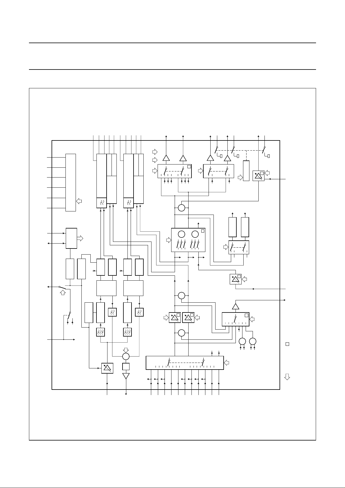
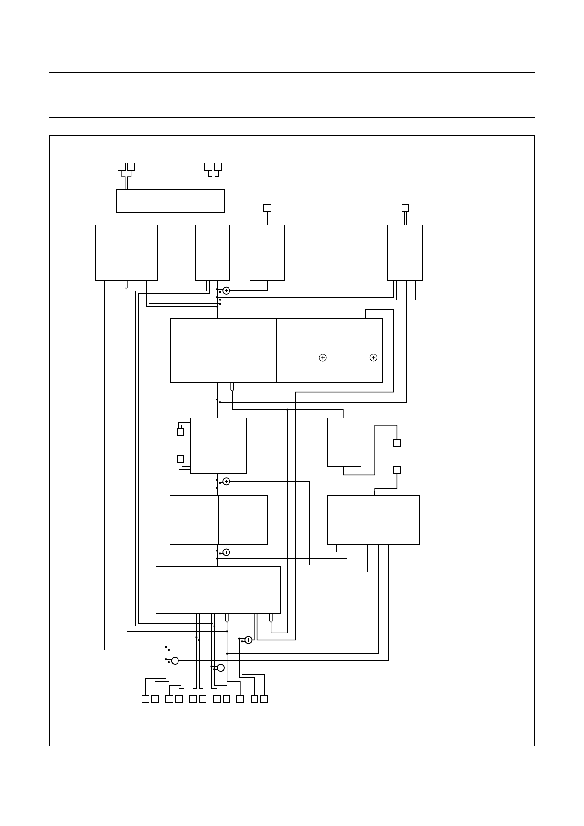
BLOCK DIAGRAM
MUTEC
DCFBL23DCREFL24EMPHL25DCL26DETL
DCFBR33DCREFR32EMPHR31DCR
DETR
DECL
DECR
LINEL
MUTEL
LINER
MUTER
RFCOUT
ref
I
ref
V
38 29 28
V5OUT
AGND DGND
35 27 43
CC
V
SDA SCL
ndbook, full pagewidth
ENVOUT
envelope
40 39 41 42
HID
select
output
SUPPLY
C-BUS
2
I
INTERFACE
HI-FI
DETECTOR
+ playback
DCL
DCR
standby mode
DROPOUT
CANCELING
HID
22
noise reduction
HID
LEVEL
DETECTOR
CCA
audio
SAMPLE-
AND-HOLD
PLL
CCO
(1.3 or
HF LIMITER
1.3 or 1.4 MHz
34
RECTIFIER
DETECTOR
noise reduction
WEIGHTING AND
FM DE-EMPHASIS
HID
AUDIO
CLIPPER
SAMPLE-
1.4 MHz)
HF
+
M
CCA
RECTIFIER
WEIGHTING AND
audio
AUDIO
AND-HOLD
PLL
CCO
(1.7 or
1.8 MHz)
HF LIMITER
1.7 or 1.8 MHz
ratio
carrier
30
+1 dB 12 V
DETECTOR
decoder select
FM DE-EMPHASIS
TDA9615H
CLIPPER
HF
SAP
TUL
18
E1L
TUL
output select
volume left
TUR
SAP
19
M
E1R
SAP
TUR
L
R
line select
dub
M
+
N
15
E2L
14
16
select + record
envelope output
17
E2R
DCL
PEAK HOLD
L
mute
M
12
AUTO-MUTE
DCR
PEAK HOLD
R
level
input
normal
13
M
MGK471
mute
RF-converter
11
RFCAGC
Fig.1 Block diagram.
+ ++
M
M
volume right
+
N
dub
E1L
E1R
E2L
E2R
SAP
TUL
input select
+
TUR
M
normal select
+
E2L
E2R
20 21
LINOUT LININ
= mute
M
C-bus data and
2
control signals
I
44
1
SAP
TUNL
2
TUNR
37
FMIN
36
FMOUT
1997 Jun 16 3
3
4
5
6
7
8
9
10
CINL
CINR
EXT1L
EXT1R
EXT2L
EXT2R
AUXL
AUXR
Philips Semiconductors Preliminary specification
Audio processor for VHS hi-fi TDA9615H
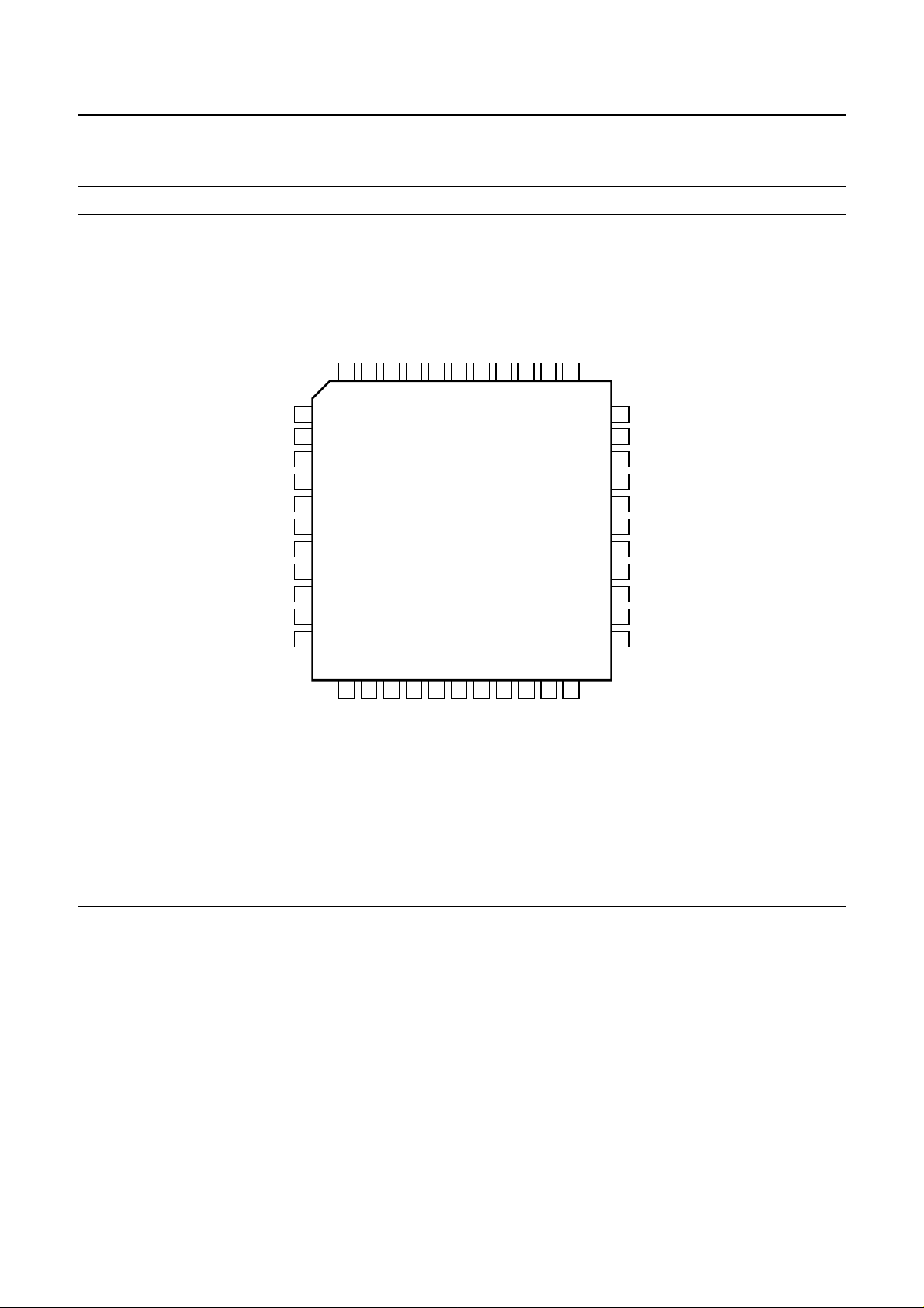
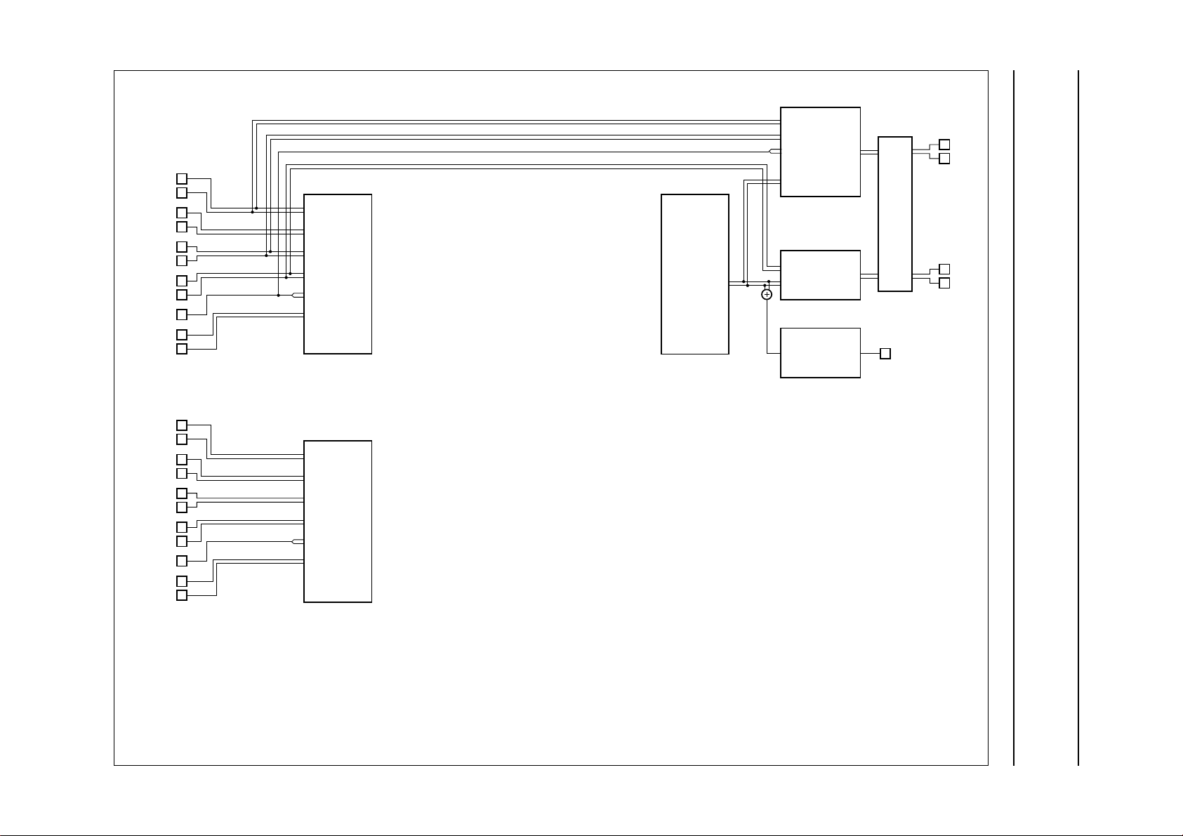
PINNING
SYMBOL PIN DESCRIPTION
TUNL 1 tuner input left
TUNR 2 tuner input right
CINL 3 cinch input left
CINR 4 cinch input right
EXT1L 5 external 1 input left
EXT1R 6 external 1 input right
EXT2L 7 external 2 input left
EXT2R 8 external 2 input right
AUXL 9 auxiliary input left
AUXR 10 auxiliary input right
RFCAGC 11 RFC AGC timing input
RFCOUT 12 RFC output
MUTEC 13 mute for RFC output
MUTEL 14 mute for line output left
LINEL 15 line output left
LINER 16 line output right
MUTER 17 mute for line output right
DECL 18 decoder output left
DECR 19 decoder output right
LINOUT 20 linear audio output
LININ 21 linear audio input
DCFBL 22 NR DC feedback left
SYMBOL PIN DESCRIPTION
DCREFL 23 NR DC reference left
EMPHL 24 NR emphasis left
DCL 25 NR DC decoupling left
DETL 26 NR detector left
AGND 27 analog ground
I
ref
V
ref
28 reference current standard
29 reference voltage filter
DETR 30 NR detector right
DCR 31 NR DC decoupling right
EMPHR 32 NR emphasis right
DCREFR 33 NR DC reference right
DCFBR 34 NR DC feedback right
V
CC
35 supply voltage
FMOUT 36 FM output
FMIN 37 FM input
V5OUT 38 5 V decoupling output
ENVOUT 39 envelope output
HID 40 HID input
SDA 41 I
SCL 42 I
2
C-bus SDA input/output
2
C-bus SCL input
DGND 43 digital ground
SAP 44 tuner SAP input
1997 Jun 16 4
Philips Semiconductors Preliminary specification
Audio processor for VHS hi-fi TDA9615H
handbook, full pagewidth
TUNL
TUNR
CINL
CINR
EXT1L
EXT1R
EXT2L
EXT2R
AUXL
AUXR
RFCAGC
SCL
DGND
43
42
13
14
MUTEL
MUTEC
SDA
HID
41
40
TDA9615H
15
16
LINEL
LINER
SAP
44
1
2
3
4
5
6
7
8
9
10
11
12
RFCOUT
V5OUT
ENVOUT
39
383736
17
18
DECL
MUTER
FMIN
19
DECR
CC
FMOUT
V
35
21
20
LININ
LINOUT
DCFBR
34
22
DCFBL
33
32
31
30
29
28
27
26
25
24
23
MGK470
DCREFR
EMPHR
DCR
DETR
V
ref
I
ref
AGND
DETL
DCL
EMPHL
DCREFL
Fig.2 Pin configuration.
FUNCTIONAL DESCRIPTION
An overview of input/output selections is given in Figs 3 to 5.
Full control of the TDA9615H is accomplished via the 2-wire I2C-bus. Up to 400 kbits/s bus speed can be used, in
accordance with the I2C-bus fast-mode specification. The detailed functional description can be found in
Chapter “I2C-bus protocol”.
1997 Jun 16 5
Philips Semiconductors Preliminary specification
Audio processor for VHS hi-fi TDA9615H
k, full pagewidth
DECL
LOH
decoder select
TUNER
EXT1
DECR
SAP
MUTE
OUTPUT SELECT
0 dB
+1 dB
output select
MUTE
FMIN
tape
FMOUT
LINEL
line select
EXT2
LEFT
RIGHT
LINER
OUTPUT SELECT
STEREO
NORMAL
HI-FI
AUDIO FM
PROCESSING
RFC mute
0 dB AGC
NORMAL LEFT
NORMAL RIGHT
RFCOUT
MUTE
NORMAL STEREO
ENVOUT
envelope select
OUTPUT SELECT
STEREO
normal input levelnormal select
MGK473
HF ENVELOPEHF envelope
MUTE
(0 to +14 dB)
LININ
processing
linear audio
LINOUT
input select
TUNL
TUNR
volume left
CINCH
TUNER
CINL
CINR
MUTE
(−47 to 0 dB;
EXT1
EXT1L
0 to +15 dB)
EXT1R
EXT2
EXT2L
MUTE
SAP
EXT2R
0 to +15 dB)
(−47 to 0 dB;
DUB MIX
AUX
SAP
AUXL
NORMAL
(1)
AUXR
1997 Jun 16 6
volume right
INPUT SELECT
INPUT LEFT
VOLUME
VOLUME LEFT
SAP
TUNER
EXT2
MUTE
Fig.3 Input/output selections; standard operation.
(1) For ‘Dub Mix’ mode signal selections see Fig.4.
Philips Semiconductors Preliminary specification
Audio processor for VHS hi-fi TDA9615H
ull pagewidth
DECL
LOH
decoder select
TUNER
EXT1
SAP
DECR
MUTE
0 dB
+1 dB
OUTPUT SELECT
MUTE
FMIN
tape
FMOUT
LINEL
line select
LEFT
RIGHT
LINER
EXT2
OUTPUT SELECT
STEREO
NORMAL
HI-FI
AUDIO FM
PROCESSING
RFC mute
NORMAL
NORMAL
(playback)
RFCOUT
0 dB AGC
MUTE
NORMAL
MUTE
LEFT
RIGHT
LEFT RIGHT
normal input levelnormal select
LEFT
NORMAL
MUTE
(0 to +14 dB)
RIGHT
envelope select
OUTPUT SELECT
LEFT RIGHT
ENVOUT
HF ENVELOPEHF envelope
STEREO
LININ
processing
linear audio
LINOUT
MGK474
(record)
EXT2L
EXT2R
MUTE
0 to +15 dB)
(−47 to 0 dB;
SAP
DUB MIX
AUXL
AUXR
volume hi-fi
input select
TUNL
TUNR
MUTE
volume aux output select
CINL
CINR
0 to +15 dB)
(−47 to 0 dB;
EXT1L
EXT1R
1997 Jun 16 7
INPUT SELECT
INPUT LEFT
VOLUME
VOLUME LEFT
SAP
TUNER
EXT2
MUTE
Fig.4 Input/output selections; ‘Dub Mix’ mode.
‘Dub Mix’ mode (IS2= 1; IS1= 0; IS0= 1); input mixing of hi-fi (‘playback’ mode) signal with AUX input for linear audio recording (audio dubbing).
Selections generally used in combination with this mode are shown in heavy line type.
1997 Jun 16 8
p
agewidth
Philips Semiconductors Preliminary specification
Audio processor for VHS hi-fi TDA9615H
decoder select
TUNL
TUNR
CINL
CINR
EXT1L
EXT1R
EXT2L
EXT2R
SAP
AUXL
AUXR
input select
MUTE
output select
MUTE
TUNER
EXT1
SAP
MUTE
OUTPUT SELECT
line select
EXT2
OUTPUT SELECT
RFC mute
0 dB AGC
MUTE
LOH
0 dB
+1 dB
RFCOUT
DECL
DECR
LINEL
LINER
TUNL
TUNR
CINL
CINR
EXT1L
EXT1R
EXT2L
EXT2R
SAP
AUXL
AUXR
a. Active standby mode (STBA = 1, STBP = 0); 75% power reduction.
input select
MUTE
b. Passive standby mode (STBP = 1); 90% power reduction.
Fig.5 Input/output selections; standby modes.
MGK475
Philips Semiconductors Preliminary specification
Audio processor for VHS hi-fi TDA9615H
I2C-BUS PROTOCOL
Addressing and data bytes
For programming the device (write mode) seven data byte registers are available; they are addressable via eight
subaddresses. Automatic subaddress incrementing enables the writing of successive data bytes in one transmission.
During power-on, data byte registers are reset to a default state by use of a Power On Reset (POR) circuit which signal
is derived from the internally generated I
one data byte register is available without subaddressing.
Table 1 TDA9615H addresses and data bytes
DATA BYTE ADDRESS
Write mode
Slave address byte (B8H) 1 0111000
Subaddress bytes (00H to 07H) 0
Control byte (subaddress 00) AFM DOC SHH DETH NTSC MUTE STBP STBA
Select byte (subaddress 01) DOS1 DOS0 s5 s4 NIL3 NIL2 NIL1 NIL0
Input byte (subaddress 02) i7 IS2 IS1 IS0 NS2 NS1 NS0 i0
Output byte (subaddress 03) LOH OSN OSR OSL EOS LOS DOS RFCM
Left volume byte
(subaddress 04)
Right volume byte
(subaddress 05)
Volume byte (subaddress 06) simultaneous loading of subaddress 04 and subaddress 05 register
Power byte (subaddress 07) CALS VCCH TEST PORR p3 p2 p1 p0
2
C-bus supply voltage (V5OUT; pin 38). For reading from the device (read mode)
(1)
(1)
0
(1)
0
(1)
0
0 0 or 1 0 or 1 0 or 1
I7 VLS VL5 VL4 VL3 VL2 VL1 VL0
r7 VRS VR5 VR4 VR3 VR2 VR1 VR0
Read mode
Slave address byte (B9H) 1 0111001
Read byte CALR AUTN 0
(2)
POR 0
(2)
(2)
1
(2)
0
(2)
0
Notes
1. Use of subaddress F0H to F7H (1111 0XXX) instead of 00H to 07H (0000 0XXX) disables the automatic subaddress
incrementing allowing continuous writing to a single data byte register.
2. The state of unused read bits are not reliable; their state may change during development.
Table 2 Status of data bytes after POR
DATA BYTE ADDRESS
Control byte 1 0001100
Select byte 0 0 1
Input byte 0
(1)
0001110
(1)
(1)
1
0000
(1)
Output byte 0 0000001
Left volume byte 0
Right volume byte 0
Power byte 0 0000
(1)
(1)
1000000
1000000
(1)
(1)
0
(1)
0
(1)
0
Note
1. For eventual future compatibility it is advised to keep unused write bits equal to POR state.
1997 Jun 16 9
Philips Semiconductors Preliminary specification
Audio processor for VHS hi-fi TDA9615H
Valid transmissions to and from TDA9615H
Table 3 Examples of valid transmissions
FUNCTION DATA TRANSFER SEQUENCE
Write START - B8H - 00H - data_for_00 - STOP
Write with auto-increment START - B8H - 00H - data_for_00 - data_for_01 - data_for_02 - STOP
Auto-increment ‘wrap-around’ START - B8H - 07H - data_for_07 - data_for_00 - data_for_01 - STOP
Write without auto-increment START - B8H - F6H - data_for_06 - data_for_06 - data_for_06 - STOP
Read START - B9H - data_from_ic - STOP
START - B9H - data_from_ic - data_from_ic - data_from_ic - STOP
2
Overview of TDA9615H I
Table 4 Condensed overview
FUNCTION MODES CONTROL BITS
Audio FM mode playback; loop-through
Dropout cancelling on; off DOC
Headswitch noise cancel
sample-and-hold time
Playback hi-fi carrier detection slow; fast DETH
Record carrier ratio 0; 6; 8; 9.5; 11; 12.5; 13.5 dB DOC, SHH and DETH
System standard NTSC
Power mute output muting
Operation mode full operation
Normal input level 0
Input select Tuner
Normal select Input Select; Volume; Input-Left; Volume-Left; SAP;
Line output amplification 0 dB
Output select mute
Envelope output Output Select
Line output select Output Select
Decoder output select Output Select
RFC output 0 dB; mute
Volume left −47 to 0 dB
Volume right −47 to 0 dB
Auto-calibration off
Supply voltage 9 V
Test standard operation
C-bus control
6 µs; 8 µs SHH
(1)
to +14 dB; mute NIL3 to NIL0
Tuner; Ext2; mute
(1)
(1)
Mix-Stereo
(1)
; start calibration CALS
(1)
(1)
; record AFM, DOC and SHH
(1)
; PAL NTSC
(1)
(1)
; active standby; passive standby STBP and STBA
(1)
; Cinch; Ext1; Ext2; SAP; Dub Mix; Normal; Aux IS2, IS1 and IS0
MUTE
NS2, NS1 and NS0
(1)
; +1 dB LOH
; Left; Right; Stereo; Normal; Mix-Left; Mix-Right;
(1)
; Stereo; HF Envelope EOS and AFM
(1)
; Ext2 LOS
(1)
; Tuner; Ext1; SAP; mute DOS, DOS1 and DOS0
(1)
(1)
; 0 to +15 dB; mute VLS, VL5 to VL0
(1)
; 0 to +15 dB; mute VRS, VR5 to VR0
OSN, OSR and OSL
RFCM
; 12 V VCCH
(1)
; test modes TEST, s4 to NIL0
Note
1. POR.
1997 Jun 16 10
Philips Semiconductors Preliminary specification
Audio processor for VHS hi-fi TDA9615H
Control byte; subaddress 00 (hi-fi and general control)
Table 5 Bits of control byte
BIT DESCRIPTION
AFM audio FM mode; see Table 6
DOC dropout cancel; see Table 6
SHH sample-and-hold high-state; see Table 6
DETH detector high; see Table 6
NTSC NTSC television system standard; see Table 7
MUTE power mute; see Table 8
STBP standby mode passive; see Table 9
STBA standby mode active; see Table 9
Table 6 Bits AFM, DOC, SHH and DETH
AFM DOC SHH DETH MODE REMARKS DESCRIPTION
0X
(1)
00X
01X
0X
0X
0X
0X
1X
(1)
(1)
(1)
(1)
(1)
1000loop-through
1001record 0 dB mix 0 dB FM output carrier ratio (1 : 1)
1010record 6 dB mix 6 dB FM output carrier ratio (1 : 2)
1011record 8 dB mix 8 dB FM output carrier ratio (1 : 2.5)
1100record 9.5 dB mix standard 9.5 dB FM output carrier ratio (1 : 3)
1101record 11 dB mix 11 dB FM output carrier ratio (1 : 3.5)
1110record 12.5 dB mix 12.5 dB FM output carrier ratio (1 : 4.2)
1111record 13.5 dB mix 13.5 dB FM output carrier ratio (1 : 4.7)
(1)
X
(1)
(1)
0X
1X
(1)
X
(1)
X
(1)
X
(1)
X
(1)
X
(1)
X
(1)
(1)
0 playback detect = fast hi-fi detector timing: fast mode
1 playback detect = slow hi-fi detector timing: slow mode
(1)
X
playback
(2)
hi-fi circuit in playback mode
playback DOC off no dropout cancelling
playback DOC on dropout cancelling active
playback sample-and-
headswitch noise cancel time is 6 µs
hold time = 6 µs
playback sample-and-
headswitch noise cancel time is 8 µs
hold time = 8 µs
record/loop-through hi-fi circuit in record/loop-through mode
(3)(4)
no FM output signal (EE mode)
Notes
1. X = don’t care.
2. Auto-normal function: if during hi-fi ‘playback’ mode no FM carrier is detected at FMIN (pin 37) the ‘Normal’ mode
audio signal (LININ; pin 21) is automatically selected by the output select function.
a) Hi-fi carrier detection time (i.e. auto-normal release time) can be selected via bit DETH:
‘fast’ mode: 1 to 2 HID periods (33 to 66 ms NTSC, 40 to 80 ms PAL)
‘slow’ mode: 7 to 8 HID periods (233 to 267 ms NTSC, 280 to 320 ms PAL).
2
b) The status of hi-fi detection can be monitored via the I
C-bus; see bit AUTN of the read byte (see Table 31).
c) If muting is required instead of automatic selection of the ‘Normal’ mode audio signal the normal input level
function should be set to mute; see bits NIL3 to NIL0 of the select byte.
1997 Jun 16 11
Philips Semiconductors Preliminary specification
Audio processor for VHS hi-fi TDA9615H
3. Modes ‘loop-through’ and ‘record’ are equal in audio signal flow; FMOUT (pin 36) however is muted during
‘loop-through’ mode.
4. POR.
Table 7 Bit NTSC
(1)
NTSC
0 PAL hi-fi circuit in ‘PAL’ mode (FM carriers: 1.4and 1.8 MHz)
1 NTSC
Notes
1. Bit NTSC selects between the system standard settings for NTSC and PAL (SECAM) use. The auto-calibration
function uses the system standard HID frequency of 29.97 Hz for NTSC and 25 Hz for PAL. After calibration bit NTSC
allows immediate switching between the NTSC and PAL system standard.
2. POR.
Table 8 Bit MUTE
MUTE
0 − power mute function released; mute switches open
1 mute
MODE DESCRIPTION
(2)
hi-fi circuit in ‘NTSC’ mode (FM carriers: 1.3 and 1.7 MHz)
(1)
MODE DESCRIPTION
(2)
power mute function activated; mute switches closed
Notes
1. Bit MUTE controls the line and RFC output mute switches at pins 13, 14 and 17 (power mute function). Power mute
is also automatically activated at supply voltage power-up or power-down (VCC; pin 35).
2. POR.
Table 9 Bits STBP and STBA
STBP STBA MODE DESCRIPTION
00− (note 1) full operation
01
(4)
1
(2)
(5)
X
active standby
passive standby
(3)
(3)
standby mode; reduced power consumption
standby mode; minimum power consumption
Notes
1. POR.
2. By selecting STBA = 1 the TDA9615H is switched to low-power ‘active standby’ mode. To reduce power
consumption most circuits are switched off. RFC, line and decoder outputs however remain active. This way the
direct audio selections offered via the line output select and decoder output select functions (bits LOS and DOS of
the output byte) remain operable in this mode. The ‘Output Select’ mode signal is muted.
3. Calibration and I
2
C-bus registers are not affected by using ‘active standby’ or ‘passive standby’ mode.
4. By selecting STBP = 1 the TDA9615H is switched to minimum power ‘passive standby’ mode. All circuits except
power mute, I2C-bus and the line input reference buffer (voltage at pins 1 to 10 and 44) are switched off for minimum
power consumption. Use of the power mute function (bit MUTE of control byte) ensures pop-free switching of the line
and RFC output to and from ‘passive standby’ mode. To obtain minimum power consumption the power mute
function should be de-activated again during ‘passive standby’ mode.
5. X = don’t care.
1997 Jun 16 12
Philips Semiconductors Preliminary specification
Audio processor for VHS hi-fi TDA9615H
Select byte; subaddress 01 (decoder output select and linear audio volume control)
Table 10 Bits of select byte
BIT DESCRIPTION
DOS1 decoder output select 1; see Table 11
DOS0 decoder output select 0; see Table 11
NIL3 normal input level 3; see Table 12
NIL2 normal input level 2; see Table 12
NIL1 normal input level 1; see Table 12
NIL0 normal input level 0; see Table 12
Table 11 Bits DOS1 and DOS0; note 1
DOS1 DOS0 MODE DESCRIPTION
0 0 Tuner decoder output signal is TUNL and TUNR input signal
0 1 Ext1 decoder output signal is EXT1L and EXT1R input signal
1 0 SAP decoder output signal is SAP input signal
1 1 mute mute
Note
1. By selecting bit DOS = 1 of the output byte several independent signal input selections are offered for the decoder
outputs DECL and DECR (pins 18 and 19) via bits DOS1 and DOS0:
a) TUNL and TUNR inputs (pins 1 and 2)
b) EXT1L and EXT1R inputs (pins 5 and 6)
c) SAP input (pin 44)
d) Mute.
These decoder selections are also operable in ‘active standby’ mode (bit STBA = 1 of the control byte).
1997 Jun 16 13
Philips Semiconductors Preliminary specification
Audio processor for VHS hi-fi TDA9615H
Table 12 Bits NIL3, NIL2, NIL1 and NIL0; note 1
NIL3 NIL2 NIL1 NIL0 DESCRIPTION
00000dB; note 2
00011dB
00102dB
00113dB
01004dB
01015dB
01106dB
01117dB
10008dB
10019dB
101010dB
101111dB
110012dB
110113dB
111014dB
1111mute
Notes
1. Mute and 15 settings of amplification can be selected for the linear audio input signal (LININ; pin 21). This level
control can replace the manual adjustment of ‘playback’ mode level at the linear audio circuit.
2. POR.
Input byte; subaddress 02 (input selection for hi-fi and normal audio)
Table 13 Bits of input byte
BIT DESCRIPTION
IS2 input select 2; see Table 14
IS1 input select 1; see Table 14
IS0 input select 0; see Table 14
NS2 normal select 2; see Table 15
NS1 normal select 1; see Table 15
NS0 normal select 0; see Table 15
1997 Jun 16 14
 Loading...