


INTEGRATED CIRCUITS
DEVICE SPECIFICATION
DATA SH EET
TDA935X/6X/8X PS/N2 series
TV signal processor-Teletext
decoder with embedded µ-Controller
Tentative Device Specification
File under Integrated Circuits, <Handbook>
Version: 2.8
Previous date: 2000 Nov 29
2001 Jan 18

Philips Semiconductors Tentative Device Specification
TV signal processor-Teletext decoder
with embedded µ-Controller
GENERAL DESCRIPTION
The various versions of theTDA935X/6X/8X PS/N2 series
combine the functions of a TV signal processor together
with a µ-Controller and US Closed Caption decoder. Most
versions have a Teletext decoder on board. The Teletext
decoderhasaninternal RAMmemory for1or 10page text.
The ICs are intended to be used in economy television
receivers with 90° and 110° picture tubes.
The ICs have supply voltages of 8 V and 3.3 V and they
are mounted in S-DIP envelope with 64 pins.
The features are given in the following feature list. The
differences between the various ICs are given in the table
on page 4.
TDA935X/6X/8X PS/N2 series
FEATURES
TV-signal processor
• Multi-standard vision IF circuit with alignment-free PLL
demodulator
• Internal (switchable) time-constant forthe IF-AGC circuit
• A choice can be made between versions with mono
intercarrier sound FM demodulator and versions with
QSS IF amplifier.
• The mono intercarrier sound versions have a selective
FM-PLL demodulator which can be switched to the
different FM sound frequencies (4.5/5.5/6.0/6.5 MHz).
The quality of this system is such that the external
band-pass filters can be omitted.
• Source selection between ‘internal’ CVBS and external
CVBS or Y/C signals
• Integrated chrominance trap circuit
• Integrated luminance delay line with adjustable delay
time
• Picture improvement features with peaking (with
variable centre frequency and positive/negative
overshoot ratio) and black stretching
• Integrated chroma band-pass filter with switchable
centre frequency
• Only one reference (12 MHz) crystal required for the
µ-Controller, Teletext- and the colour decoder
• PAL/NTSC or multi-standard colour decoder with
automatic search system
• Internal base-band delay line
• RGB control circuit with ‘Continuous Cathode
Calibration’, white point and black level offset
adjustment so that the colour temperature of the dark
and the light parts of the screen can be chosen
independently.
• Linear RGB or YUV input with fast blanking for external
RGB/YUV sources. The Text/OSD signals are internally
supplied from the µ-Controller/Teletext decoder
• Contrast reduction possibility during mixed-mode of
OSD and Text signals
• Horizontal synchronization with two control loops and
alignment-free horizontal oscillator
• Vertical count-down circuit
• Vertical driver optimized for DC-coupled vertical output
stages
• Horizontal and vertical geometry processing
• Horizontal and vertical zoom function for 16 : 9
applications
• Horizontal parallelogram and bow correction for large
screen picture tubes
• Low-power start-up of the horizontal drive circuit
2001 Jan 18 2

Philips Semiconductors Tentative Device Specification
TV signal processor-Teletext decoder with
embedded µ-Controller
µ-Controller
• 80C51 µ-controller core standard instruction set and
timing
• 1 µs machine cycle
• 32 - 128Kx8-bit late programmed ROM
• 3 - 12Kx8-bit Auxiliary RAM (shared with Display and
Acquisition)
• Interrupt controller for individual enable/disable with two
level priority
• Two 16-bit Timer/Counter registers
• One 16 bit Timer with 8-bit Pre-scaler
• WatchDog timer
• Auxiliary RAM page pointer
• 16-bit Data pointer
• Stand-by, Idle and Power Down (PD) mode
• 14 bits PWM for Voltage Synthesis Tuning
• 8-bit A/D converter
• 4 pins which can be programmed as general I/O pin,
ADC input or PWM (6-bit) output
Data Capture
• Text memory for 0, 1 or 10 pages
• Inthe 10page versionsinventory oftransmitted Teletext
pages stored in the Transmitted Page Table (TPT) and
Subtitle Page Table (SPT)
• Data Capture for US Closed Caption
• Data Capture for 525/625 line WST, VPS (PDC system
A) and Wide Screen Signalling (WSS) bit decoding
• Automatic selection between 525 WST/625 WST
• Automatic selection between 625 WST/VPS on line 16
of VBI
• Real-time capture and decoding for WST Teletext in
Hardware, to enable optimized µ-processor throughput
• Automatic detection of FASTEXT transmission
• Real-time packet 26 engine in Hardware for processing
accented, G2 and G3 characters
• Signal quality detector for video and WST/VPS data
types
• Comprehensive teletext language coverage
• Full Field and Vertical Blanking Interval (VBI) data
capture of WST data
TDA935X/6X/8X PS/N2 series
Display
• Teletext and Enhanced OSD modes
• Features of level 1.5 WST and US Close Caption
• Serial and Parallel Display Attributes
• Single/Double/Quadruple Width and Height for
characters
• Scrolling of display region
• Variable flash rate controlled by software
• Enhanced display features including overlining,
underlining and italics
• Soft colours using CLUT with 4096 colour palette
• Globally selectable scan lines per row (9/10/13/16) and
character matrix [12x10, 12x13, 12x16 (VxH)]
• Fringing (Shadow) selectable from N-S-E-W direction
• Fringe colour selectable
• Meshing of defined area
• Contrast reduction of defined area
• Cursor
• Special Graphics Characters with two planes, allowing
four colours per character
• 32 software redefinable On-Screen display characters
• 4 WST Character sets (G0/G2) in single device (e.g.
Latin, Cyrillic, Greek, Arabic)
• G1 Mosaic graphics, Limited G3 Line drawing
characters
• WST Character sets and Closed Caption Character set
in single device
2001 Jan 18 3

2001 Jan 18 4
FUNCTIONAL DIFFERENCE BETWEEN THE VARIOUS IC VERSIONS
IC VERSION (TDA) 9350935193529353936093619362936393649365936693679380 9381 9382 9383 938493859386938793889389
TV range 90° 90° 90° 110° 90° 90° 110° 110° 110° 110° 90° 90° 90° 90° 90° 110° 110° 110° 110° 90° 110° 110°
Mono intercarrier multi-standard
sound demodulator (4.5 - 6.5 MHz)
with switchable centre frequency
Audio switch √√ √√√√√ √√ √√ √√
Automatic Volume Levelling √√√ √√ √√√√√ √
Automatic Volume Levelling or
subcarrier output (for comb filter
applications)
QSS sound IF amplifier with
separate input and AGC circuit
AM sound demodulator without
extra reference circuit
PAL decoder √√√√√√√√√√√√√√√√√√√
SECAM decoder √√√√√√√√√√√
NTSC decoder √√√√√√√√√√√√√√√√√√√√√√
Horizontal geometry (E-W) √ √√√√ √√√√ √√
Horizontal and Vertical Zoom √ √√√√ √√√√ √√
ROM size 32-
User RAM size 1 k 1 k 1 k 1 k 2 k 2 k 2 k 2 k 2 k 2 k 2 k 2 k 1 k 1 k 1 k 1 k 1 k 1 k 1 k 1 k 1 k 1 k
Teletext 1
Closed captioning √√√√√√√√√√√√√√√√√√√√√√
√√ √√√√√ √√ √√ √√
√ √√√√ √√√√ √√
√ √√√√√√√√
√√
32-
32-
32-
64-
64-
64-
64-
64-
64-
64-
64-
16-
16-
16-
16-
16-
16-
16-
16-
16-
64 k
64 k
64 k
64 k
128k
128k
128k
128k
128k
128k
128k
128k
64 k
64 k
64 k
64 k
64 k
64 k
64 k
64 k
64 k
page1page1page1page10page10page10page10page10page10page10page10page
16-
64 k
Philips Semiconductors Tentative Device Specification
TV signal processor-Teletext decoder with
embedded µ-Controller
TDA935X/6X/8X PS/N2 series

Philips Semiconductors Tentative Device Specification
TV signal processor-Teletext decoder with
TDA935X/6X/8X PS/N2 series
embedded µ-Controller
QUICK REFERENCE DATA
SYMBOL PARAMETER MIN. TYP. MAX. UNIT
Supply
V
P
I
P
Input voltages
V
iVIFrms)
V
iSIF(rms)
V
iAUDIO(rms)
V
iCVBS(p-p)
V
iCHROMA(p-p)
V
iRGB(p-p)
V
iYIN(p-p)
V
iUVIN(p-p)
Output signals
V
o(IFVO)(p-p)
V
o(QSSO)(rms)
V
o(AMOUT)(rms)
I
o(AGCOUT)
V
oRGB(p-p)
I
oHOUT
I
oVERT
I
oEWD
supply voltages − 8.0/3.3 − V
supply current − tbf − mA
video IF amplifier sensitivity (RMS value) − 75 −µV
QSS sound IF amplifier sensitivity (RMS value) − 60 −µV
external audio input (RMS value) − 500 − mV
external CVBS/Y input (peak-to-peak value) − 1.0 − V
external chroma input voltage (burst amplitude)
− 0.3 − V
(peak-to-peak value)
RGB inputs (peak-to-peak value) − 0.7 − V
luminance input signal (peak-to-peak value) − 1.4 − V
U/V input signal (peak-to-peak value) − 1.33/1.05 − V
demodulated CVBS output (peak-to-peak value) − 2.5 − V
sound IF intercarrier output in QSS versions (RMS value) − 100 − mV
demodulated AM sound output in QSS versions (RMS
− 500 − mV
value)
tuner AGC output current range 0 − 5mA
RGB output signal amplitudes (peak-to-peak value) − 2.0 − V
horizontal output current 10 −−mA
vertical output current (peak-to-peak value) 1 −−mA
EW drive output current 1.2 −−mA
2001 Jan 18 5
Philips Semiconductors Tentative Device Specification
TV signal processor-Teletext decoder with
embedded µ-Controller
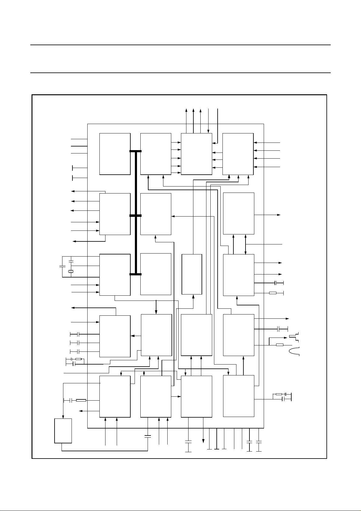
BLOCK DIAGRAM
61
+3.3 V
SDASCL
54 56
12
9
I/O PORTS (4x)
5-8
ADC IN (4x)
VST OUT
34
2
10/11
LED OUT (2x)
1/10 PAGE
MEMORY
1+62-64
C-BUS
2
I
TRANSCEIVER
VST PWM-DAC
I/O PORTS
DISPLAY
TELETEXT/OSD
V
H
TELETEXT
ACQUISITION
CVBS
SYNC
ROGOB0
515253
BL
B
RG
COR
CCC
CONTR/BRIGHTN
OSD/TEXT INSERT
TDA935X/6X/8X PS/N2 series
BLKIN
BCLIN
49
50
45
484746
GB
R
WHITE-P. ADJ.
RGB/YUV INSERT
SATURATION
RGB/YUV MATRIX
YUV/RGB MATRIX
Y
U
V
(20)
(EW GEOMETRY)
36
G/Y B/U BL
R/V
EWD
EHTO
TRAP
SOUND
VPE
RESET
AUDOUT
AUDEXT
SNDIF
TUNERAGC
60 55 59 58 57
44
35
29 28
(20)
31
(32)
27 37 38
(32)
80C51 CPU
ENHANCED
(AVL)
DEEMPHASIS
AUDIO SWITCH
VOLUME CONTROL
AGC/AFC
VISION IF
23
VIDEO AMP.
PLL DEMOD.
ALIGNMENT-FREE
24
IFIN
ROM/RAM
PLL
AGC CIRCUIT
NARROW BAND
DEMODULATOR
VIDEO IDENT.
VIDEO SWITCH
VIDEO FILTERS
42
40
43
CHROMA
CVBS/Y
PEAKING
LUMA DELAY
BASE-BAND
REF
REF
PAL/SECAM/NTSC
13
BLACK STRETCH
DELAY LINE
DECODER
30
41
(32)
18
V-DRIVE +
GEOMETRY
V
LOOP
nd
H-SHIFT
H-DRIVE
2
H
H-OSC. + PLL
H/V SYNC SEP.
19
39
14
+8V
21
222625
33
16
34
HOUT V-DRIVE
Fig. 1 Block diagram TDA935X/6X8X PS/N2 with mono intercarrier sound demodulator
17
15
2001 Jan 18 6
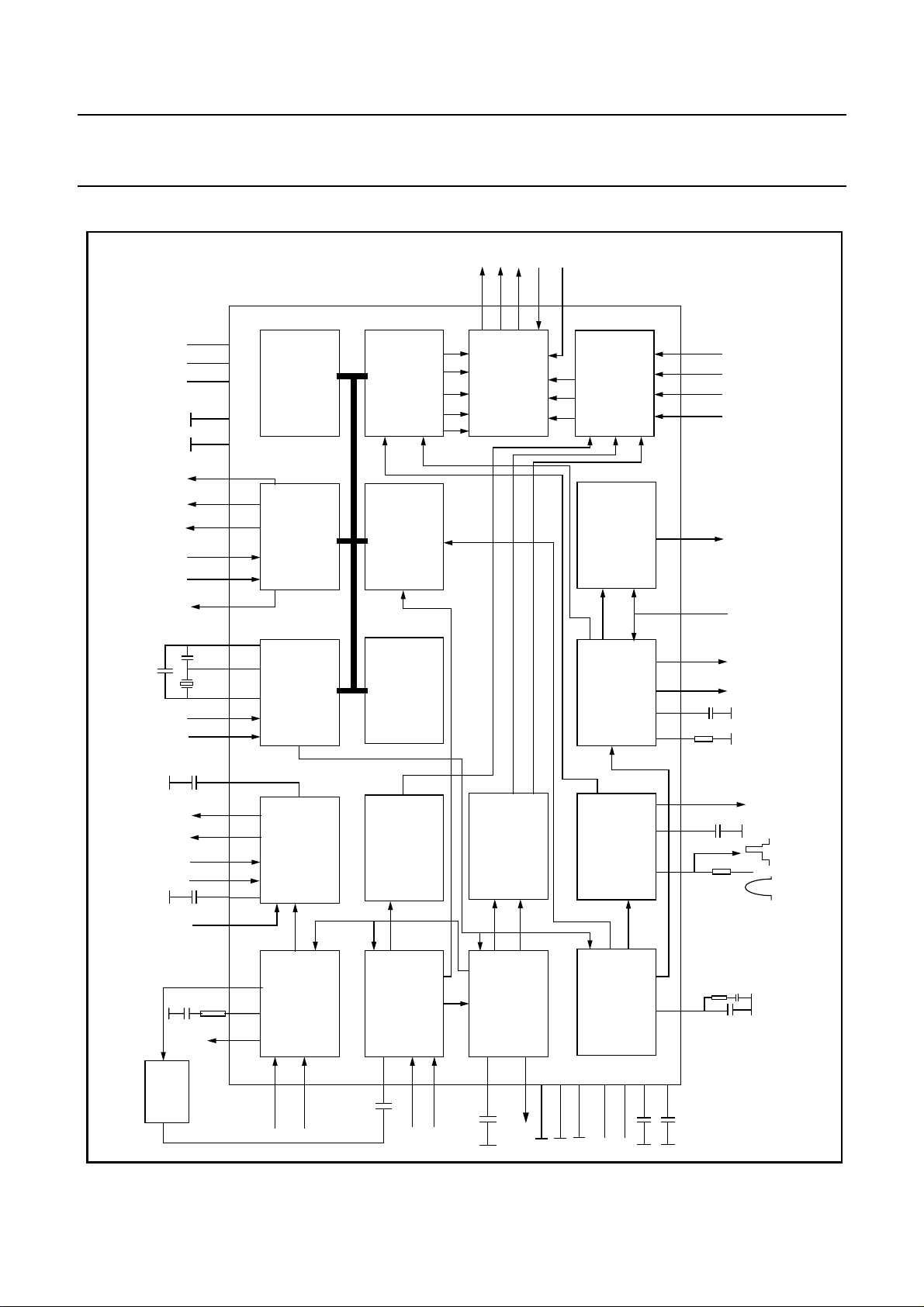
Philips Semiconductors Tentative Device Specification
TV signal processor-Teletext decoder with
embedded µ-Controller
ROGOBO
515253
DISPLAY
BL
B
RG
CONTR/BRIGHTN
COR
SYNC
+3.3 V
I/O PORTS (4x)
ADC IN (4x)
VST OUT
SDASCL
LED OUT (2x)
61
54 56
12
9
1+62-64
5-8
C-BUS
34
2
I
2
10/11
10 PAGE
MEMORY
I/O PORTS
TRANSCEIVER
VST PWM-DAC
TELETEXT/OSD
V
H
TELETEXT
ACQUISITION
CVBS
TDA935X/6X/8X PS/N2 series
BLKIN
BCLIN
49
50
45
484746
CCC
OSD/TEXT INSERT
GB
R
WHITE-P. ADJ.
RGB/YUV INSERT
SATURATION
RGB/YUV MATRIX
YUV/RGB MATRIX
Y
U
V
(20)
EW GEOMETRY
36
G/Y B/U BL
R/V
EWD
EHTO
TRAP
SOUND
VPE
60 55 59 58 57
RESET
31
AMOUT
(35) 44
QSSOUT/AMOUT
SIFIN
28 29
AUDEXT
(35)
27 37 38
TUNERAGC
ENHANCED
(32)
(20)
QSS SOUND IF
VISION IF
ALIGNMENT-FREE
23
80C51 CPU
AGC
QSS MIXER
AM DEMODULTOR
AGC/AFC
VIDEO AMP.
PLL DEMOD.
24
IFIN
ROM/RAM
PEAKING
LUMA DELAY
REF
VIDEO IDENT.
VIDEO SWITCH
42
40
CVBS/Y
BLACK STRETCH
VIDEO FILTERS
43
CHROMA
BASE-BAND
REF
PAL/SECAM/NTSC
13
DELAY LINE
DECODER
30
41
(32)
V-DRIVE +
V
LOOP
nd
H-DRIVE
2
H/V SYNC SEP.
39
18
14
+8V
21
222625
GEOMETRY
3334
16
H-SHIFT
H
17
H-OSC. + PLL
19
15
HOUT V-DRIVE
Fig. 2 Block diagram TDA 935X/6X/8X PS/N2 with QSS IF sound channel
2001 Jan 18 7

Philips Semiconductors Tentative Device Specification
TV signal processor-Teletext decoder with
TDA935X/6X/8X PS/N2 series
embedded µ-Controller
PINNING
SYMBOL PIN DESCRIPTION
P1.3/T1 1 port 1.3 or Counter/Timer 1 input
2
P1.6/SCL 2 port 1.6 or I
P1.7/SDA 3 port 1.7 or I2C-bus data line
P2.0/TPWM 4 port 2.0 or Tuning PWM output
P3.0/ADC0 5 port 3.0 or ADC0 input
P3.1/ADC1 6 port 3.1 or ADC1 input
P3.2/ADC2 7 port 3.2 or ADC2 input
P3.3/ADC3 8 port 3.3 or ADC3 input
VSSC/P 9 digital ground for µ-Controller core and periphery
P0.5 10 port 0.5 (8 mA current sinking capability for direct drive of LEDs)
P0.6 11 port 0.6 (8 mA current sinking capability for direct drive of LEDs)
VSSA 12 analog ground of Teletext decoder and digital ground of TV-processor
SECPLL 13 SECAM PLL decoupling
VP2 14 2nd supply voltage TV-processor (+8V)
DECDIG 15 decoupling digital supply of TV-processor
PH2LF 16 phase-2 filter
PH1LF 17 phase-1 filter
GND3 18 ground 3 for TV-processor
DECBG 19 bandgap decoupling
AVL/EWD
(1)
20 Automatic Volume Levelling /East-West drive output
VDRB 21 vertical drive B output
VDRA 22 vertical drive A output
IFIN1 23 IF input 1
IFIN2 24 IF input 2
IREF 25 reference current input
VSC 26 vertical sawtooth capacitor
TUNERAGC 27 tuner AGC output
AUDEEM/SIFIN1
DECSDEM/SIFIN2
(1)
28 audio deemphasis or SIF input 1
(1)
29 decoupling sound demodulator or SIF input 2
GND2 30 ground 2 for TV processor
SNDPLL/SIFAGC
AVL/SNDIF/REF0/
AMOUT
(1)
(1)
31 narrow band PLL filter /AGC sound IF
32 Automatic Volume Levelling / sound IF input / subcarrier reference output /AM output
(non controlled)
HOUT 33 horizontal output
FBISO 34 flyback input/sandcastle output
AUDEXT/
QSSO/AMOUT
(1)
35 external audio input /QSS intercarrier out /AM audio output (non controlled)
EHTO 36 EHT/overvoltage protection input
PLLIF 37 IF-PLL loop filter
IFVO/SVO 38 IF video output / selected CVBS output
VP1 39 main supply voltage TV-processor (+8 V)
CVBSINT 40 internal CVBS input
GND1 41 ground 1 for TV-processor
CVBS/Y 42 external CVBS/Y input
CHROMA 43 chrominance input (SVHS)
AUDOUT /AMOUT
(1)
44 audio output /AM audio output (volume controlled)
C-bus clock line
2001 Jan 18 8
Philips Semiconductors Tentative Device Specification
TV signal processor-Teletext decoder with
TDA935X/6X/8X PS/N2 series
embedded µ-Controller
SYMBOL PIN DESCRIPTION
INSSW2 45 2nd RGB / YUV insertion input
R2/VIN 46 2nd R input / V (R-Y) input
G2/YIN 47 2nd G input / Y input
B2/UIN 48 2nd B input / U (B-Y) input
BCLIN 49 beam current limiter input / (V-guard input, note 2)
BLKIN 50 black current input / (V-guard input, note 2)
RO 51 Red output
GO 52 Green output
BO 53 Blue output
VDDA 54 analog supply of Teletext decoder and digital supply of TV-processor (3.3 V)
VPE 55 OTP Programming Voltage
VDDC 56 digital supply to core (3.3 V)
OSCGND 57 oscillator ground supply
XTALIN 58 crystal oscillator input
XTALOUT 59 crystal oscillator output
RESET 60 reset
VDDP 61 digital supply to periphery (+3.3 V)
P1.0/INT1 62 port 1.0 or external interrupt 1 input
P1.1/T0 63 port 1.1 or Counter/Timer 0 input
P1.2/INT0 64 port 1.2 or external interrupt 0 input
Note
1. The function of pin 20, 28, 29, 31, 32, 35 and 44 is dependent on the IC version (mono intercarrier FM demodulator
/ QSS IF amplifier and East-West output or not) and on some software control bits. The valid combinations are given
in table 1.
2. The vertical guard function can be controlled via pin 49 or pin 50. The selction is made by means of the IVG bit in
subaddress 2BH.
Table 1 Pin functions for various versions
IC version FM-PLL version QSS version
East-West Y/N N Y N Y
CMB1/CMB0 bits 00 01/10/11 00 01/10/11 00 01/10/11 00 01/10/11
AM bit −− − −−01 −01
Pin 20 AVL EWD AVL EWD
Pin 28 AUDEEM SIFIN1
Pin 29 DECSDEM SIFIN2
Pin 31 SNDPLL SIFAGC
Pin 32 SNDIF
(1)
REFO
(2)
AVL/SNDIF
(1)
REFO
(2)
AMOUT REFO
(2)
AMOUT REFO
(2)
Pin 35 AUDEXT AUDEXT QSSO AMOUT AUDEXT QSSO AMOUT
Pin 44 AUDOUT controlled AM or audio out
Note
1. When additional (external) selectivity is required for FM-PLL system pin 32 can be used as sound IF input. This
function is selected by means of SIF bit in subaddress 28H.
2. The reference output signal is only available for the CMB1/CMB0 setting of 0/1. For the other settings this pin is a
switch output (see also table 67).
2001 Jan 18 9

Philips Semiconductors Tentative Device Specification
TV signal processor-Teletext decoder with
embedded µ-Controller
handbook, halfpage
P1.3/T1
P1.6/SCL
P1.7/SDA
P2.0/TPMW
P3.0/ADC0
P3.1/ADC1
P3.2/ADC2
P3.3/ADC3
VSSC/P
P0.5
P0.6
VSSA
SECPLL
VP2
DECDIG
PH2LF
PH1LF
GND3
DECBG
AVL/EWD
VDRB
VDRA
IFIN1
IFIN2
IREF
VSC
TUNERAGC
AUDEEM/SIFIN1
DECSDEM/SIFIN2
GND2
SNDPLL/SIFAGC
AVL/SNDIF/
REFO/AMOUT
1
2
3
4
5
6
7
8
9
10
11
12
13
14
15
16
XXX
17
18
19
20
21
22
23
24
25
26
27
28
29
30
31
32
TDA935X/6X/8X PS/N2
MXXxxx
TDA935X/6X/8X PS/N2 series
64
P1.2/INT0
63
P1.1/T0
62
P1.0/INT1
61
VDDP
60
RESET
59
XTALOUT
58
XTALIN
OSCGND
57
56
VDDC
55
VPE
54
VDDA
53
BO
52
GO
51
RO
50
BLKIN
49
BCLIN
48
B2/UIN
47
G2/YIN
46
R2/VIN
45
INSSW2
44
AUDOUT/AMOUT
43
CHROMA
42
CVBS/Y
41
GND1
40
CVBSINT
39
VP1
38
IFVO/SVO
37
PLLIF
36
EHTO
AUDEXT/QSSO/
35
AMOUT
34
FBISO
33
HOUT
Fig. 3 Pin configuration (SDIP 64)
2001 Jan 18 10
Philips Semiconductors Tentative Device Specification
TV signal processor-Teletext decoder with
embedded µ-Controller
FUNCTIONAL DESCRIPTION OF THE 80C51
The functionality of the micro-controller used on this
device is described here with reference to the industry
standard 80C51 micro-controller. A full description of its
functionality can be found in the 80C51 based 8-bit
micro-controllers - Philips Semiconductors (ref. IC20).
Features of the 80c51
• 80C51micro-controllercore standardinstructionset and
timing.
• 1µs machine cycle.
• Maximum 128K x 8-bit Program ROM.
• Maximum of 12K x 8-bit Auxiliary RAM.
• 2K (OSD only version) Auxiliary RAM, maximum
of 1.25K required for Display
• 3K (1 page teletext version) Auxiliary RAM,
maximum of 2K required for Display
• 12K (10 page teletext version) Auxiliary RAM,
maximum of 10K required for Display
• 8-Level Interrupt Controller for individual enable/disable
with two level priority.
• Two 16-bit Timer/Counters.
• Additional 16-bit Timer with 8-bit Pre-scaler.
• WatchDog Timer.
• Auxiliary RAM Page Pointer.
• 16-bit Data pointer
• Idle, Stand-by and Power-Down modes.
• 13 General I/O.
• Four 6-bit Pulse Width Modulator (PWM) outputs for
control of TV analogue signals.
• One 14-bit PWM for Voltage Synthesis tuner control.
• 8-bit ADC with 4 multiplexed inputs.
• 2 high current outputs for directly driving LED’s etc.
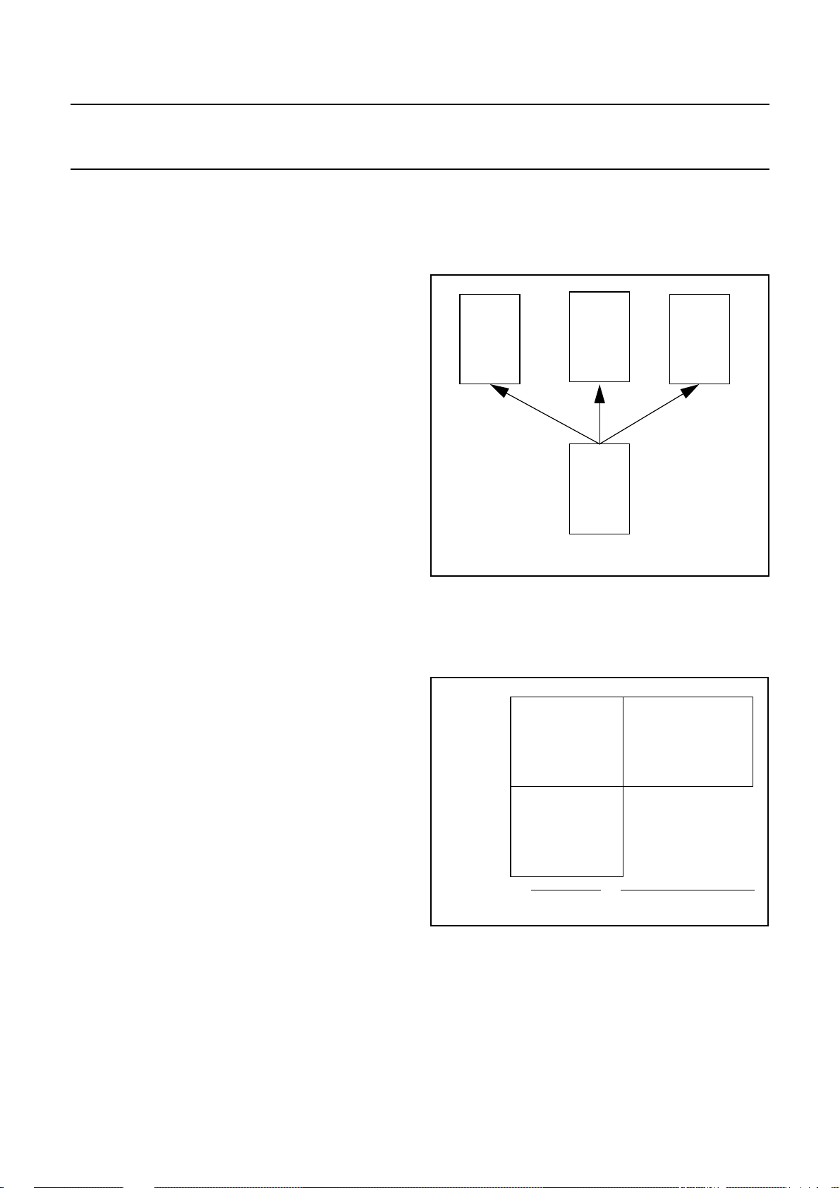
• I2C Byte Level bus interface.
TDA935X/6X/8X PS/N2 series
the 32K banks is common and is always addressable.The
other three banks (Bank0, Bank1, Bank2) can be
accessed by selecting the right bank via the SFR ROMBK
bits 1/0.
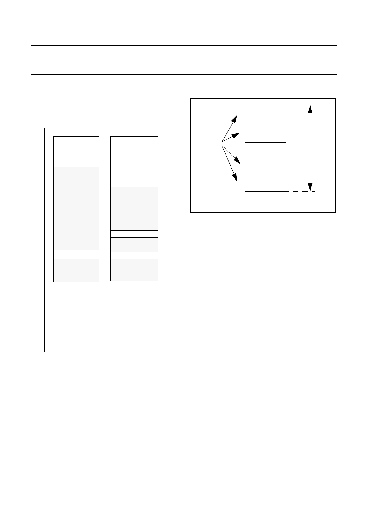
FFFFH
Bank0
32K
8000H
Fig.4 ROM Bank Switching memory map
RAM Organisation
The Internal Data RAM is organised into two areas, Data
Memory and Special Function Registers (SFRs) as shown
in Fig.5.
FFH
Upper
128
80H
7FH
Lower
128
FFFFH
Bank1
8000H
7FFFH
Common
0000H
Accessible
by Indirect
Addressing
only
Accessible
by Direct
and Indirect
Addressing
32K
32K
FFFFH
Bank2
32K
8000H
Accessible
by Direct
Addressing
only
Memory Organisation
Thedevice has thecapability of a maximum of128K Bytes
of PROGRAM ROM and 12K Bytes of DATA RAM. The
OSD (& Closed Caption) only version has a 2K RAM and
a maximum of 64K ROM, the 1 page teletext version has
a 3K RAM and also a maximum of 64K ROM whilst the 10
page teletext version has a 12K RAM and a maximum of
128K ROM.
ROM Organisation
The 64K device has a continuous address space from 0 to
64K. The 128K is arranged in four banks of 32K. One of
2001 Jan 18 11
00H
Data Memory Special Function Registers
Fig.5 Internal Data Memory
DATA MEMORY
TheData memoryis 256 x 8-bits andoccupies theaddress
range00 to FF Hex when using Indirectaddressing and00
to7F Hexwhen using directaddressing. TheSFRs occupy
the address range 80 Hex to FF Hex and are accessible
using Direct addressing only. The lower 128 Bytes of Data
memory are mapped as shown in Fig.6. The lowest 32
Philips Semiconductors Tentative Device Specification
TV signal processor-Teletext decoder with
TDA935X/6X/8X PS/N2 series
embedded µ-Controller
bytes are grouped into 4 banks of 8 registers, the next 16 bytes above the register banks form a block of bit addressable
memory space. The upper 128 bytes are not allocated for any special area or functions.
7FH
Bank Select
Bits in PSW
11 = BANK3
10 = BANK2
01 = BANK1
00 = BANK0
Fig.6 Lower 128 Bytes of Internal RAM
2FH
20H
1FH
18H
17H
10H
0FH
08H
07H
00H
(Bit Addresses 0-7F)
Bit Addressable Space
R0 - R7
4 Banks of 8 Registers
SFR MEMORY
TheSpecial Function Register(SFR) space is used forport latches, counters/timers, peripheral control, data capture and
display. These registers can only be accessed by direct addressing. Sixteen of the addresses in the SFR space are both
bit and byte addressable. The bit addressable SFRs are those whose address ends in 0H or 8H. A summary of the SFR
map in address order is shown in Table 2.
ADD R/W Names BIT7 BIT6 BIT5 BIT4 BIT3 BIT2 BIT1 BIT0
80H R/W P0 Reserved P0<6> P0<5> Reserved Reserved Reserved Reserved Reserved
81H R/W SP SP<7> SP<6> SP<5> SP<4> SP<3> SP<2> SP<1> SP<0>
82H R/W DPL DPL<7> DPL<6> DPL<5> DPL<4> DPL<3> DPL<2> DPL<1> DPL<0>
83H R/W DPH DPH<7> DPH<6> DPH<5> DPH<4> DPH<3> DPH<2> DPH<1> DPH<0>
84H R/W IEN1 -------ET2
85H R/W IP1 -------PT2
87H R/W PCON 0 ARD RFI WLE GF1 GF0 PD IDL
88H R/W TCON TF1 TR1 TF0 TR0 IE1 IT1 IE0 IT0
89H R/W TMOD GATE C/TM1M0GATEC/TM1M0
8AH R/W TL0 TL0<7> TL0<6> TL0<5> TL0<4> TL0<3> TL0<2> TL0<1> TL0<0>
8BH R/W TL1 TL1<7> TL1<6> TL1<5> TL1<4> TL1<3> TL1<2> TL1<1> TL1<0>
8CH R/W TH0 TH0<7> TH0<6> TH0<5> TH0<4> TH0<3> TH0<2> TH0<1> TH0<0>
8DH R/W TH1 TH1<7> TH1<6> TH1<5> TH1<4> TH1<3> TH1<2> TH1<1> TH1<0>
90H R/W P1 P1<7> P1<6> Reserved Reserved P1<3> P1<2> P1<1> P1<0>
91H R/W TP2L TP2L<7> TP2L<6> TP2L<5> TP2L<4> TP2L<3> TP2L<2> TP2L<1> TP2L<0>
Table 2 SFR Map
2001 Jan 18 12

Philips Semiconductors Tentative Device Specification
TV signal processor-Teletext decoder with
TDA935X/6X/8X PS/N2 series
embedded µ-Controller
ADD R/W Names BIT7 BIT6 BIT5 BIT4 BIT3 BIT2 BIT1 BIT0
92H R/W TP2H TP2H<15> TP2H<14> TP2H<13> TP2H<12> TP2H<11> TP2H<10> TP2H<9> TP2H<8>
93H R/W TP2PR TP2PR<7> TP2PR<6> TP2PR<5> TP2PR<4> TP2PR<3> TP2PR<2> TP2PR<1> TP2PR<0>
94H R/W TP2CRL ------TP2CRL<1> TP2CRL<0>
96H R/W P0CFGA Reserved
97H R/W P0CFGB Reserved P0CFGB<6> P0CFGB<5> Reserved Reserved Reserved Reserved Reserved
98H R/W SADB - - - DC_COMP SAD<3> SAD<2> SAD<1> SAD<0>
9CH R TP2CL TP2CL<7> TP2CL<6> TP2CL<5> TP2CL<4> TP2CL<3> TP2CL<2> TP2CL<1> TP2CL<0>
9DH R TP2CH TP2CH<7> TP2CH<6> TP2CH<5> TP2CH<4> TP2CH<3> TP2CH<2> TP2CH<1> TP2CH<0>
9EH R/W P1CFGA
9FH R/W P1CFGB P1CFGB<7> P1CFGB<6> Reserved Reserved P1CFGB<3> P1CFGB<2> P1CFGB<1> P1CFGB<0>
A0H R/W P2 Reserved ------P2<0>
A6H R/W P2CFGA Reserved
A7H R/W P2CFGB Reserved P2CFGB<6> P2CFGB<5> P2CFGB<4> P2CFGB<3> P2CFGB<2> P2CFGB<1> P2CFGB<0>
P1CFGA<7> P1CFGA<6>
P0CFGA<6> P0CFGA<5>
Reserved Reserved
P2CFGA<6> P2CFGA<5> P2CFGA<4> P2CFGA<3> P2CFGA<2> P2CFGA<1> P2CFGA<0>
Reserved Reserved Reserved Reserved Reserved
P1CFGA<3> P1CFGA<2> P1CFGA<1> P1CFGA<0>
A8H R/W IE EA EBUSY ES2 ECC ET1 EX1 ET0 EX0
B0H R/W P3 Reserved Reserved Reserved Reserved P3<3> P3<2> P3<1> P3<0>
B2H R/W TXT18 NOT<3> NOT<2> NOT<1> NOT<0> 0 0 BS<1> BS<0>
B3H R/W TXT19 TEN TC<2> TC<1> TC<0> 0 0 TS<1> TS<0>
B4H R/W TXT20 DRCS
B5H R/W TXT21 DISP
B6H R TXT22 GPF1<7> GPF1<6> GPF1<5> GPF1<4> GPF1<3> GPF1<2> GPF1<1> GPF1<0>
B7H R/W CCLIN 0 0 0 CS<4> CS<3> CS<2> CS<1> CS<0>
B8H R/W IP 0 PBUSY PES2 PCC PT1 PX1 PT0 PX0
B9H R/W TXT17 0 FORCE
BAH R WSS1 0 0 0 WSS<3:0>
BBH R WSS2 0 0 0 WSS<7:4>
BCH R WSS3
BEH R/W P3CFGA Reserved Reserved Reserved Reserved
ENABLE
LINE<1>
WSS<13:11>
ERROR
OSD
PLANES
DISP
LINES<0>
ACQ<1>
WSS<13> WSS<12> WSS<11> WSS<10:8>
0 0 OSDLANG
CHAR
SIZE<1>
FORCE
ACQ<0>
CHAR
SIZE<0>
FORCE
DISP<1>
ERROR
ERROR
P3CFGA<3> P3CFGA<2> P3CFGA<1> P3CFGA<0>
ENABLE
Reserved CC ON I2C PORT0 CC/TXT
FORCE
DISP<0>
WSS<3> WSS<2> WSS<1> WSS<0>
WSS<7> WSS<6> WSS<5> WSS<4>
ERROR
OSD
LAN<2>
SCREEN
COL<2>
WSS<10> WSS<9> WSS<8>
OSD
LAN<1>
SCREEN
COL<1>
OSD
LAN<0>
SCREEN
COL<0>
BFH R/W P3CFGB Reserved Reserved Reserved Reserved P3CFGB<3> P3CFGB<2> P3CFGB<1> P3CFGB<0>
C0H R/W TXT0 X24 POSN DISPLAY
X24
AUTO
FRAME
DISABLE
HEADER
ROLL
DISPLAY
STATUS
ROW ONLY
DISABLE
FRAME
VPS ON INV ON
Table 2 SFR Map
2001 Jan 18 13

Philips Semiconductors Tentative Device Specification
TV signal processor-Teletext decoder with
TDA935X/6X/8X PS/N2 series
embedded µ-Controller
ADD R/W Names BIT7 BIT6 BIT5 BIT4 BIT3 BIT2 BIT1 BIT0
C1H R/W TXT1 EXT PKT
OFF
C2H R/W TXT2 ACQ BANK REQ<3> REQ<2> REQ<1> REQ<0> SC<2> SC<1> SC<0>
C3H W TXT3 - - - PRD<4> PRD<3> PRD<2> PRD<1> PRD<0>
C4H R/W TXT4 OSDBANK
ENABLE
C5H R/W TXT5 BKGND
OUT
C6H R/W TXT6 BKGND
OUT
C7H R/W TXT7 STATUS
ROW TOP
C8H R/W TXT8 (Reserved)
0
C9H R/W TXT9 CURSOR
FREEZE
8 BIT ACQ OFF X26 OFF FULL
QUAD
WIDTH
ENABLE
BKGND IN CORB OUT CORB IN TEXT OUT TEXT IN PICTURE
BKGND IN CORB OUT CORB IN TEXT OUT TEXT IN PICTURE
CURSOR
ON
FLICKER
STOP ON
CLEAR
MEMORY
WES
EAST/
T
REVEAL BOTTOM/
HUNT DISABLE
A0 R<4> R<3> R<2> R<1> R<0>
DISABLE
DOUBLE
HEIGHT
TOP
SPANISH
FIELD
B MESH
ENABLE
DOUBLE
HEIGHT
PKT 26
RECEIVED
FIELD
POLARITYHPOLARITYVPOLARITY
C MESH
ENABLE
BOX ON 24 BOX ON
WSS
RECEIVED
TRANS
ENABLE
ON OUT
ON OUT
1-23
WSS ON CVBS1/
SHADOW
ENABLE
PICTURE
ON IN
PICTURE
ON IN
BOX ON 0
CVBS0
CAH R/W TXT10 0 0 C<5> C<4> C<3> C<2> C<1> C<0>
CBH R/W TXT11 D<7> D<6> D<5> D<4> D<3> D<2> D<1> D<0>
CCH R TXT12 525/
CDH R/W TXT14 0 0 0 DISPLAY
CEH R/W TXT15 0 0 0 MICRO
D0H R/W PSW C AC F0 RS1 RS0 OV - P
D2H R/W TDACL TD<7> TD<6> TD<5> TD<4> TD<3> TD<2> TD<1> TD<0>
D3H R/W TDACH TPWE 1 TD<13> TD<12> TD<11> TD<10> TD<9> TD<8>
D5H R/W PWM0 PW0E 1 PW0V<5> PW0V<4> PW0V<3> PW0V<2> PW0V<1> PW0V<0>
D6H R/W PWM1 PW1E 1 PW1V<5> PW1V<4> PW1V<3> PW1V<2> PW1V<1> PW1V<0>
D7H R CCDAT1 CCD1<7> CCD1<6> CCD1<5> CCD1<4> CCD1<3> CCD1<2> CCD1<1> CCD1<0>
D8H R/W S1CON CR<2> ENSI STA STO SI AA CR<1> CR<0>
D9H R S1STA STAT<4> STAT<3> STAT<2> STAT<1> STAT<0> 0 0 0
DAH R/W S1DAT DAT<7> DAT<6> DAT<5> DAT<4> DAT<3> DAT<2> DAT<1> DAT<0>
DBH R/W S1ADR ADR<6> ADR<5> ADR<4> ADR<3> ADR<2> ADR<1> ADR<0> GC
625
SYNC
ROM
VER<4>
ROM
VER<3>
ROM
VER<2>
BANK
BANK
ROM
VER<1>
PAGE<3> PAGE<2> PAGE<1> PAGE<0>
BLOCK<3> BLOCK<2> BLOCK<1> BLOCK<0>
ROM
VER<0>
1 VIDEO
SIGNAL
QUALITY
DCH R/W PWM3 PW3E 1 PW3V<5> PW3V<4> PW3V<3> PW3V<2> PW3V<1> PW3V<0>
E0H R/W ACC ACC<7> ACC<6> ACC<5> ACC<4> ACC<3> ACC<2> ACC<1> ACC<0>
E4H R/W PWM2 PW2E 1 PW2V<5> PW2V<4> PW2V<3> PW2V<2> PW2V<1> PW2V<0>
Table 2 SFR Map
2001 Jan 18 14
Philips Semiconductors Tentative Device Specification
TV signal processor-Teletext decoder with
TDA935X/6X/8X PS/N2 series
embedded µ-Controller
ADD R/W Names BIT7 BIT6 BIT5 BIT4 BIT3 BIT2 BIT1 BIT0
E7H R CCDAT2 CCD2<7> CCD2<6> CCD2<5> CCD2<4> CCD2<3> CCD2<2> CCD2<1> CCD2<0>
E8H R/W SAD VHI CH<1> CH<0> ST SAD<7> SAD<6> SAD<5> SAD<4>
F0H R/W B B<7> B<6> B<5> B<4> B<3> B<2> B<1> B<0>
F8H R/W TXT13 VPS
RECEIVED
FAH R/W XRAMP XRAMP<7> XRAMP<6> XRAMP<5> XRAMP<4> XRAMP<3> XRAMP<2> XRAMP<1> XRAMP<0>
FBH R/W ROMBK STANDBY
FDH R TEST TEST<7> TEST<6> TEST<5> TEST<4> TEST<3> TEST<2> TEST<1> TEST<0>
FEH W WDTKEY WKEY<7> WKEY<6> WKEY<5> WKEY<4> WKEY<3> WKEY<2> WKEY<1> WKEY<0>
FFH R/W WDT WDV<7> WDV<6> WDV<5> WDV<4> WDV<3> WDV<2> WDV<1> WDV<0>
Table 2 SFR Map
A description of each of the SFR bits is shown in Table 3, The SFRs are in alphabetical order.
PAGE
CLEARING
IIC_LUT<1> IIC_LUT<0>
525
DISPLAY
525 TEXT 625 TEXT PKT 8/30 FASTEXT 0
0 0 0 ROMBK<1> ROMBK<0>
Names ADD BIT7 BIT6 BIT5 BIT4 BIT3 BIT2 BIT1 BIT0 RESET
ACC E0H ACC<7> ACC<6> ACC<5> ACC<4> ACC<3> ACC<2> ACC<1> ACC<0> 00H
ACC<7:0> Accumulator value.
B F0H B<7> B<6> B<5> B<4> B<3> B<2> B<1> B<0> 00H
B<7:0> B Register value.
CCDAT1 D7H CCD1<7> CCD1<6> CCD1<5> CCD1<4> CCD1<3> CCD1<2> CCD1<1> CCD1<0> 00H
CCD1<7:0> Closed Caption first data byte.
CCDAT2 E7H CCD2<7> CCD2<6> CCD2<5> CCD2<4> CCD2<3> CCD2<2> CCD2<1> CCD2<0> 00H
CCD2<7:0> Closed Caption second data byte.
CCLIN B7H 0 0 0 CS<4> CS<3> CS<2> CS<1> CS<0> 15H
CS<4:0> Closed Caption Slice line using 525 line number.
DPH 83H DPH<7> DPH<6> DPH<5> DPH<4> DPH<3> DPH<2> DPH<1> DPH<0> 00H
DPH<7:0> Data Pointer High byte, used with DPL to address display and auxiliary memory.
DPL 82H DPL<7> DPL<6> DPL<5> DPL<4> DPL<3> DPL<2> DPL<1> DPL<0> 00H
DPL<7:0> Data pointer low byte, used with DPH to address display and auxiliary memory.
IE A8H EA EBUSY ES2 ECC ET1 EX1 ET0 EX0 00H
EA Disable all interrupts (0), or use individual interrupt enable bits (1).
EBUSY Enable BUSY Interrupt.
ES2 Enable I
ECC Enable Closed Caption Interrupt.
2
C Interrupt.
Table 3 SFR Bit description
2001 Jan 18 15

Philips Semiconductors Tentative Device Specification
TV signal processor-Teletext decoder with
TDA935X/6X/8X PS/N2 series
embedded µ-Controller
Names ADD BIT7 BIT6 BIT5 BIT4 BIT3 BIT2 BIT1 BIT0 RESET
ET1 Enable Timer 1 Interrupt.
EX1 Enable External Interrupt 1.
ET0 Enable Timer 0 Interrupt.
EX0 Enable External Interrupt 0.
IEN1 84H-------ET200H
ET2 Enable Timer 2 Interrupt.
IP B8H 0 PBUSY PES2 PCC PT1 PX1 PT0 PX0 00H
PBUSY Priority EBUSY Interrupt.
PES2 Priority ES2 Interrupt.
PCC Priority ECC Interrupt.
PT1 Priority Timer 1 Interrupt.
PX1 Priority External Interrupt 1.
PT0 Priority Timer 0 Interrupt.
PX0 Priority External Interrupt 0.
IP1 85H-------PT200H
PT2 Priority Timer 2 Interrupt.
P0 80H Reserved P0<6> P0<5> Reserved Reserved Reserved Reserved Reserved FFH
P0<6:5> Port 0 I/O register connected to external pins.
P1 90H P1<7> P1<6> Reserved Reserved P1<3> P1<2> P1<1> P1<0> FFH
P1<7:6> Port 1 I/O register connected to external pins.
P1<3:0> Port 1 I/O register connected to external pins.
P2 A0H Reserved P2<6> P2<5> P2<4> P2<3> P2<2> P2<1> P2<0> FFH
P2<6:0> Port 2 I/O register connected to external pins.
P3 B0H Reserved Reserved Reserved Reserved P3<3> P3<2> P3<1> P3<0> FFH
P3<3:0> Port 3 I/O register connected to external pins.
P0CFGA 96H Reserved
P0CFGB 97H Reserved
P0CFGB<x>/P0CFGA<x> = 00 MODE 0 Open Drain.
P0CFGB<x>/P0CFGA<x> = 01 MODE 1 Quasi Bi-Directional.
P0CFGB<x>/P0CFGA<x> = 10 MODE2 High Impedance.
P0CFGA<6> P0CFGA<5>
P0CFGB<6> P0CFGB<5>
Reserved Reserved Reserved Reserved Reserved FFH
Reserved Reserved Reserved Reserved Reserved 00H
P0CFGB<x>/P0CFGA<x> = 11 MODE3 Push Pull.
P1CFGA
P1CFGB
9EH P1CFGA<7> P1CFGA<6>
9FH P1CFGB<7> P1CFGB<6>
Reserved Reserved
Reserved Reserved
Table 3 SFR Bit description
2001 Jan 18 16
P1CFGA<3> P1CFGA<2> P1CFGA<1> P1CFGA<0>
P1CFGB<3> P1CFGB<2> P1CFGB<1> P1CFGB<0>
FFH
00H

Philips Semiconductors Tentative Device Specification
TV signal processor-Teletext decoder with
TDA935X/6X/8X PS/N2 series
embedded µ-Controller
Names ADD BIT7 BIT6 BIT5 BIT4 BIT3 BIT2 BIT1 BIT0 RESET
P1CFGB<x>/P1CFGA<x> = 00 MODE 0 Open Drain.
P1CFGB<x>/P1CFGA<x> = 01 MODE 1 Quasi Bi-Directional.
P1CFGB<x>/P1CFGA<x> = 10 MODE2 High Impedance.
P1CFGB<x>/P1CFGA<x> = 11 MODE3 Push Pull.
P2CFGA A6H Reserved
P2CFGB A7H Reserved
P2CFGB<x>/P2CFGA<x> = 00 MODE 0 Open Drain.
P2CFGB<x>/P2CFGA<x> = 01 MODE 1 Quasi Bi-Directional.
P2CFGB<x>/P2CFGA<x> = 10 MODE2 High Impedance.
P2CFGB<x>/P2CFGA<x> = 11 MODE3 Push Pull.
P3CFGA BEH Reserved Reserved Reserved Reserved
P3CFGB BFH Reserved Reserved Reserved Reserved
P3CFGB<x>/P3CFGA<x> = 00 MODE 0 Open Drain.
P2CFGA<6> P2CFGA<5> P2CFGA<4> P2CFGA<3> P2CFGA<2> P2CFGA<1> P2CFGA<0>
P2CFGB<6> P2CFGB<5> P2CFGB<4> P2CFGB<3> P2CFGB<2> P2CFGB<1> P2CFGB<0>
P3CFGA<3> P3CFGA<2> P3CFGA<1> P3CFGA<0>
P3CFGB<3> P3CFGB<2> P3CFGB<1> P3CFGB<0>
FFH
00H
FFH
00H
P3CFGB<x>/P3CFGA<x> = 01 MODE 1 Quasi Bi-directional.
P3CFGB<x>/P3CFGA<x> = 10 MODE2 High Impedance.
P3CFGB<x>/P3CFGA<x> = 11 MODE3 Push Pull.
PCON 87H SMOD ARD RFI WLE GF1 GF0 PD IDL 00H
SMOD UART Baud Rate Double Control.
ARD Auxiliary RAM Disable, All MOVX instructions access the external data memory.
RFI Disable ALE during internal access to reduce Radio Frequency Interference.
WLE Watch Dog Timer enable.
GF1 General purpose flag.
GF0 General purpose flag.
PD Power-down activation bit.
IDL Idle mode activation bit.
PSW D0H C AC F0 RS<1> RS<0> OV - P 00H
C Carry Bit.
AC Auxiliary Carry bit.
F0 Flag 0, General purpose flag.
RS<1:0> Register Bank selector bits.
RS<1:0> = 00, Bank0 (00H - 07H).
RS<1:0> = 01, Bank1 (08H - 0FH).
RS<1:0> = 10, Bank2 (10H - 17H).
RS<1:0> = 11, Bank3 (18H - 1FH).
OV Overflow flag.
Table 3 SFR Bit description
2001 Jan 18 17

Philips Semiconductors Tentative Device Specification
TV signal processor-Teletext decoder with
TDA935X/6X/8X PS/N2 series
embedded µ-Controller
Names ADD BIT7 BIT6 BIT5 BIT4 BIT3 BIT2 BIT1 BIT0 RESET
P Parity bit.
PWM0 D5H PW0E 1 PW0V<5> PW0V<4> PW0V<3> PW0V<2> PW0V<1> PW0V<0> 40H
PW0E 0 - Disable Pulse Width Modulator 0.
1 - Enable Pulse Width Modulator 0.
PW0V<5:0> Pulse Width Modulator high time.
PWM1 D6H PW1E 1 PW1V<5> PW1V<4> PW1V<3> PW1V<2> PW1V<1> PW1V<0> 40H
PW1E 0 - Disable Pulse Width Modulator 1.
1 - Enable Pulse Width Modulator 1.
PW1V<5:0> Pulse Width Modulator high time.
PWM2 E4H PW2E 1 PW2V<5> PW2V<4> PW2V<3> PW2V<2> PW2V<1> PW2V<0> 40H
PW2E 0 - Disable Pulse Width Modulator 2.
1 - Enable Pulse Width Modulator 2.
PW2V<5:0> Pulse Width Modulator high time.
PWM3 DCH PW3E 1 PW3V<5> PW3V<4> PW3V<3> PW3V<2> PW3V<1> PW3V<0> 40H
PW3E 0 - Disable Pulse Width Modulator 3.
1 - Enable Pulse Width Modulator 3.
PW3V<5:0> Pulse Width Modulator high time.
ROMBK FBH STANDBY
STANDBY 0 - Disable Stand-by Mode
1 - Enable Stand-by Mode
IIC_LUT<1:0>IIC Lookup table selection:
IIC_LUT<1:0>=00, 558 Normal Mode.
IIC_LUT<1:0>=01, 558 Fast Mode.
IIC_LUT<1:0>=10, 558 Slow Mode.
IIC_LUT<1:0>=11, Reserved.
ROMBK<1:0>ROM Bank selection
ROMBK<1:0>=00, Bank0
ROMBK<1:0>=01, Bank1
ROMBK<1:0>=10, Bank2
ROMBK<1:0>=11, Reserved
S1ADR DBH ADR<6> ADR<5> ADR<4> ADR<3> ADR<2> ADR<1> ADR<0> GC 00H
ADR<6:0> I2C Slave Address.
GC 0 - Disable I2C general call address.
1 - Enable I2C general call address.
S1CON D8H CR<2> ENSI STA STO SI AA CR<1> CR<0> 00H
IIC_LUT<1> IIC_LUT<0>
000
ROMBK<1> ROMBK<0>
00H
CR<2:0> Clock rate bits.
IIC rates are selectable (three tables)
ENSI 0 - Disable I2C interface.
1 - Enable I2C interface.
Table 3 SFR Bit description
2001 Jan 18 18
Philips Semiconductors Tentative Device Specification
TV signal processor-Teletext decoder with
TDA935X/6X/8X PS/N2 series
embedded µ-Controller
Names ADD BIT7 BIT6 BIT5 BIT4 BIT3 BIT2 BIT1 BIT0 RESET
STA START flag. When this bit is set in slave mode, the hardware checks the I2C bus and generates a START condition if the bus is free or after the bus
becomes free. If the device operates in master mode it will generate a repeated START condition.
STO STOP flag. If this bit is set in a master mode a STOP condition is generated. A STOP condition detected on the I2C bus clears this bit. This bit may also
be set in slave mode in order to recover from an error condition. In this case no STOP condition is generated to the I2C bus, but the hardware releases
the SDA and SCL lines and switches to the not selected receiver mode. The STOP flag is cleared by the hardware.
SI Serial Interrupt flag. This flag is set and an interrupt request is generated, after any of the following events occur:
-A START condition is generated in master mode.
-The own slave address has been received during AA=1.
-The general call address has been received while S1ADR.GC and AA=1.
-A data byte has been received or transmitted in master mode (even if arbitration is lost).
-A data byte has been received or transmitted as selected slave.
A STOP or START condition is received as selected slave receiver or transmitter
While the SI flag is set, SCL remains LOW and the serial transfer is suspened.SI must be reset by software.
AA Assert Acknowledge flag. When this bit is set, an acknowledge is returned after any one of the following conditions
-Own slave address is received.
-General call address is received(S1ADR.GC=1).
-A data byte is received, while the device is programmed to be a master receiver.
-A data byte is received, while the device is selected slave receiver.
When the bit is reset, no acknowledge is returned. Consequently, no interrupt is requested when the own address or general call address is received.
S1DAT DAH DAT<7> DAT<6> DAT<5> DAT<4> DAT<3> DAT<2> DAT<1> DAT<0> 00H
2
DAT<7:0> I
S1STA D9H STAT<4> STAT<3> STAT<2> STAT<1> STAT<0> 0 0 0 F8H
STAT<4:0> I2C Interface Status.
SAD E8H VHI CH<1> CH<0> ST SAD<7> SAD<6> SAD<5> SAD<4> 00H
CH<1:0> ADC Input channel select.
SAD<7:4> Most Significant nibble of DAC input word
SADB 98H 0 0 0 DC_COMP SAD<3> SAD<2> SAD<1> SAD<0> 00H
DC_COMP 0 - Disable DC Comparator mode.
SAD<3:0> 4-bit SAD value.
SP 81H SP<7> SP<6> SP<5> SP<4> SP<3> SP<2> SP<1> SP<0> 07H
C Data.
VHI 0 - Analogue input voltage less than or equal to DAC voltage.
1 - Analogue input voltage greater then DAC voltage.
CH<1:0> = 00,ADC3.
CH<1:0> = 01,ADC0.
CH<1:0> = 10,ADC1.
CH<1:0> = 11,ADC2.
ST Initiate voltage comparison between ADC input Channel and SADB<3:0> value.
Note: Set by Software and reset by Hardware.
1 - Enable DC Comparator mode.
SP<7> Stack Pointer.
TCON 88H TF1 TR1 TF0 TR0 IE1 IT1 IE0 IT0 00H
TF1 Timer 1 overflow Flag. Set by hardware on Timer/Counter overflow.Cleared by hardware when processor vectors to interrupt routine.
Table 3 SFR Bit description
2001 Jan 18 19

Philips Semiconductors Tentative Device Specification
TV signal processor-Teletext decoder with
TDA935X/6X/8X PS/N2 series
embedded µ-Controller
Names ADD BIT7 BIT6 BIT5 BIT4 BIT3 BIT2 BIT1 BIT0 RESET
TR1 Timer 1 Run control bit. Set/Cleared by software to turn Timer/Counter on/off.
TF0 Timer 0 overflow Flag. Set by hardware on Timer/Counter overflow.Cleared by hardware when processor vectors to interrupt routine.
TR0 Timer 0 Run control bit. Set/Cleared by software to turn Timer/Counter on/off.
IE1 Interrupt 1 Edge flag (both edges generate flag). Set by hardware when external interrupt edge detected.Cleared by hardware when interrupt processed.
IT1 Interrupt 1 Type control bit. Set/Cleared by Software to specify edge/low level triggered external interrupts.
IE0 Interrupt 0 Edge l flag. Set by hardware when external interrupt edge detected.Cleared by hardware when interrupt processed.
IT0 Interrupt 0 Type flag.Set/Cleared by Software to specify falling edge/low level triggered external interrupts.
TDACH D3H TPWE 1 TD<13> TD<12> TD<11> TD<10> TD<9> TD<8> 40H
TPWE 0 - Disable Tuning Pulse Width Modulator.
1 - Enable Tuning Pulse Width Modulator.
TD<13:8> Tuning Pulse Width Modulator High Byte.
TDACL D2H TD<7> TD<6> TD<5> TD<4> TD<3> TD<2> TD<1> TD<0> 00H
TD<7:0> Tuning Pulse Width Modulator Low Byte.
TH0 8CH TH0<7> TH0<6> TH0<5> TH0<4> TH0<3> TH0<2> TH0<1> TH0<0> 00H
TH0<7:0> Timer 0 high byte.
TH1 8DH TH1<7> TH1<6> TH1<5> TH1<4> TH1<3> TH1<2> TH1<1> TH1<0> 00H
TH1<7:0> Timer 1 high byte.
TL0 8AH TL0<7> TL0<6> TL0<5> TL0<4> TL0<3> TL0<2> TL0<1> TL0<0> 00H
TL0<7:0> Timer 0 low byte.
TL1 8BH TL1<7> TL1<6> TL1<5> TL1<4> TL1<3> TL1<2> TL1<1> TL1<0> 00H
TL1<7:0> Timer 1 low byte.
TMOD 89H GATE C/T M1 M0 GATE C/T M1 M0 00H
Timer / Counter 1 Timer / Counter 0
GATE Gating Control Timer /Counter 1.
C/T Counter/Timer 1 selector.
M1,M0 Mode control bits Timer/Counter 1.
M1,M0 = 00, 8 bit timer or 8 bit counter with divide by 32 pre-scaler.
M1,M0 = 01, 16 bit time interval or event counter.
M1,M0 = 10, 8 bit time interval or event counter with automatic reload upon overflow. Reload value stored in TH1.
M1,M0 = 11, stopped.
GATE Gating control Timer/Counter 0.
C/T Counter/Timer 0 selector.
Table 3 SFR Bit description
2001 Jan 18 20

Philips Semiconductors Tentative Device Specification
TV signal processor-Teletext decoder with
TDA935X/6X/8X PS/N2 series
embedded µ-Controller
Names ADD BIT7 BIT6 BIT5 BIT4 BIT3 BIT2 BIT1 BIT0 RESET
M1,M0 Mode Control bits Timer/Counter 0.
M1,M0 = 00, 8 bit timer or 8 bit counter with divide by 32 pre-scaler.
M1,M0 = 01, 16 bit time interval or event counter.
M1,M0 = 10, 8 bit time interval or event counter with automatic reload upon overflow. Reload value stored in TH0.
M1,M0 = 11, one 8 bit time interval or event counter and one 8 bit time interval counter.
TP2CL 9CH TP2CL<7> TP2CL<6> TP2CL<5> TP2CL<4> TP2CL<3> TP2CL<2> TP2CL<1> TP2CL<0> 00H
TP2CL<7:0> Indicate the low byte of the Time 2 current value.
TP2CH 9DH TP2CH<7> TP2CH<6> TP2CH<5> TP2CH<4> TP2CH<3> TP2CH<2> TP2CH<1> TP2CH<0> 00H
TP2CH<7:0> Indicate the high byte of the Time 2 current value.
TP2H 92H TP2H<7> TP2H<6> TP2H<5> TP2H<4> TP2H<3> TP2H<2> TP2H<1> TP2H<0> 00H
TP2H<7:0> Timer 2 high byte, never change unless updated by the software.
TP2L 91H TP2L<7> TP2L<6> TP2L<5> TP2L<4> TP2L<3> TP2L<2> TP2L<1> TP2L<0> 00H
TP2L<7:0> Timer 2 low byte, never change unless updated by the software.
TP2PR 93H TP2PR<7> TP2PR<6> TP2PR<5> TP2PR<4> TP2PR<3> TP2PR<2> TP2PR<1> TP2PR<0> 00H
TP2H<7:0> Timer 2 Pre-scaler, never change unless updated by the software.
TP2CRL 94H------
TP2CRL<0> Timer 2 Control.
0 - Timer 2 disabled.
1 - Timer 2 enabled.
TP2CRL<1> Timer 2 Status.
0 - No Overflow.
1 - Overflow.
TEST FDH TEST<7> TEST<6> TEST<5> TEST<4> TEST<3> TEST<2> TEST<1> TEST<0> 00H
TEST<2:0> Program Type bit SEL<2:0>.
011 - Display Dram test.
001 - Acquisition1 test.
010 - Acquisition2 test
TEST<4:3> Functional test mode bits, set via mode select logic.
TEST<7:5> Dram Size.
000 - 1.5K x 16.
001 - 2K x 16.
010 - 6K x 16.
011 - 7K x 16.
100 - 12K x 16.
101 - 14K x 16.
110 - 1K x 16.
111 - 11K x 16.
TP2CRL<1> TP2CRL<0>
00H
TXT0 C0H X24 POSN DISPLAY
X24
X24 POSN 0 - Store X/24 in extension memory
1 - Store X/24 in basic page memory with packets 0 to 23
AUTO
FRAME
DISABLE
HEADER
ROLL
Table 3 SFR Bit description
2001 Jan 18 21
DISPLAY
STATUS
ROW
ONLY
DISABLE
FRAME
VPS ON INV ON 00H

Philips Semiconductors Tentative Device Specification
TV signal processor-Teletext decoder with
TDA935X/6X/8X PS/N2 series
embedded µ-Controller
Names ADD BIT7 BIT6 BIT5 BIT4 BIT3 BIT2 BIT1 BIT0 RESET
DISLAY X24 0 - Display row 24 from basic page memory
1 - Display row 24 from appropriate location in extension memory
AUTO
FRAME
DISABLE
HEADER
ROLL
DISPLAY
STATUS
ROW ONLY
DISABLE
FRAME
VPS ON 0 - VPS acquisition off
INV ON 0 - Inventory page off
TXT1 C1H EXT PKT
0 - Normal Frame output
1 - Frame output is switched off automatically if any video displayed
0 - Write rolling headers and time to current display page
1 - Disable writing of rolling headers and time to into memory
0 - Display normal page rows 0 to 24
1- Display only row 24
0 - Normal Frame output
1 - Force Frame output to be low (0)
1 - VPS acquisition on
1 - Inventory page on
8 BIT ACQ OFF ACQ OFF FULL
OFF
FIELD
FIELD
POLARITYHPOLARITYVPOLARITY
00H
EXT PKT
ACQ OFF 0 - Write requested data into display memory
X26 OFF 0 - Enable automatic processing of X/26 data
FULL FIELD 0 - Acquire CC data only on selected line.
FIELD
POLARIY
H POLARITY 0 - Hsync reference edge is positive going
V POLARITY 0 - Vsync reference edge is positive going
TXT2 C2H ACQ
ACQ_BANK 0 - Select Acquisition bank 0
REQ<3:0> Page request
0 - Acquire extension packets X/24,X/27,8/30/X
OFF
1 - Disable acquisition of extension packets
8 BIT 0 - Error check and/or correct packets 0 to 24
1 - Disable checking of packets 0 to 24 written into memory
1 - Disable writing of data into Display memory
1 - Disable automatic processing of X/26 data
1 - Acquire CC data on any TV line (for test purposes).
0 - Vsync pulse in first half of line during even field.
1 - Vsync pulse in second half of line during even field.
1 - Hsync reference edge is negative going
1 - Vsync reference edge is negative going
BANK
1 - Select Acquisition bank 1
REQ<3> REQ<2> REQ<1> REQ<0> SC<2> SC<1> SC<0> 00H
SC<2:0> Start column of page request
TXT3 C3H PRD<4> PRD<3> PRD<2> PRD<1> PRD<0> 00H
PRD<4:0> Page Request data
Table 3 SFR Bit description
2001 Jan 18 22

Philips Semiconductors Tentative Device Specification
TV signal processor-Teletext decoder with
TDA935X/6X/8X PS/N2 series
embedded µ-Controller
Names ADD BIT7 BIT6 BIT5 BIT4 BIT3 BIT2 BIT1 BIT0 RESET
TXT4 C4H OSD
OSD BANK
ENABLE
QUAD
WIDTH
ENABLE
WEST 0 - Western language selection of character codes A0 to FF
EAST/
DISABLE
DOUBLE
HEIGHT
B MESH
ENABLE
C MESH
ENABLE
TRANS
ENABLE
0 - Only alpha numeric OSD characters available, 32 locations
1 - Alternate OSD location available via graphic attribute, additional 32 location
0 - Disable display of Quadruple width characters
1 - Enable display of Quadruple width characters
1 - Eastern character selection of character codes A0 to FF
0 - Allow normal decoding of double height characters
1 - Disable normal decoding of double height characters
0 - Normal display of black background
1 - Enable meshing of black background
0 - normal display of coloured background
1 - Enable meshing of coloured background
0 - Display black background as normal
1 - Display black background as video
BANK
ENABLE
QUAD
WIDTH
ENABLE
EAST/WEST
DISABLE
DBL
HEIGHT
B MESH
ENABLE
C MESH
ENABLE
TRANS
ENABLE
SHADOW
ENABLE
00H
SHADOW
ENABLE
TXT5 C5H BKGND
BKGND OUT 0 - Background colour not displayed outside teletext boxes
BKGND IN 0 - Background colour not displayed inside teletext boxes
COR OUT 0 - COR not active outside teletext and OSD boxes
COR IN 0 - COR not active inside teletext and OSD boxes
TEXT OUT 0 - TEXT not displayed outside teletext boxes
TEXT IN 0 - TEXT not displayed inside teletext boxes
PICTURE ON
PICTURE ONIN0 - VIDEO not displayed inside teletext boxes
TXT6 C6H BKGND
0 - Disable display of shadow/fringing
1 - Display shadow/ fringe (default SE black)
OUT
1 - Background colour displayed outside teletext boxes
1 - Background colour displayed inside teletext boxes
1 - COR active outside teletext and OSD boxes
1 - COR active inside teletext and OSD boxes
1 - TEXT displayed outside teletext boxes
1 - TEXT displayed inside teletext boxes
0 - VIDEO not displayed outside teletext boxes
OUT
1 - VIDEO displayed outside teletext boxes
1 - VIDEO displayed inside teletext boxes
OUT
BKGND IN COR OUT COR IN TEXT OUT TEXT IN PICTURE
BKGND IN COR OUT COR IN TEXT OUT TEXT IN PICTURE
ON OUT
ON OUT
PICTURE
ON IN
PICTURE
ON IN
03H
03H
BKGND OUT 0 - Background colour not displayed outside teletext boxes
1 - Background colour displayed outside teletext boxes
Table 3 SFR Bit description
2001 Jan 18 23

Philips Semiconductors Tentative Device Specification
TV signal processor-Teletext decoder with
TDA935X/6X/8X PS/N2 series
embedded µ-Controller
Names ADD BIT7 BIT6 BIT5 BIT4 BIT3 BIT2 BIT1 BIT0 RESET
BKGND IN 0 - Background colour not displayed inside teletext boxes
1 - Background colour displayed inside teletext boxes
COR OUT 0 - COR not active outside teletext and OSD boxes
1 - COR active outside teletext and OSD boxes
COR IN 0 - COR not active inside teletext and OSD boxes
1 - COR active inside teletext and OSD boxes
TEXT OUT 0 - TEXT not displayed outside teletext boxes
1 - TEXT displayed outside teletext boxes
TEXT IN 0 - TEXT not displayed inside teletext boxes
1 - TEXT displayed inside teletext boxes
PICTURE ON
PICTURE ONIN0 - VIDEO not displayed inside teletext boxes
TXT7 C7H STATUS
0 - VIDEO not displayed outside teletext boxes
OUT
1 - VIDEO displayed outside teletext boxes
1 - VIDEO displayed inside teletext boxes
ROW TOP
CURSORONREVEAL BOTTOM/
TOP
DOUBLE
HEIGHT
BOX ON 24 BOX ON
1-23
BOX ON 0 00H
STATUS
ROW TOP
CURSOR ON 0 - Disable display of cursor
REVEAL 0 - Display as spaces characters in area with conceal attribute set
BOTTOM/TO
DOUBLE
HEIGHT
BOX ON 24 0 - Disable display of teletext boxes in memory row 24
BOX ON 1-23 0 - Disable display of teletext boxes in memory row 1 to 23
BOX ON 0 0 - Disable display of teletext boxes in memory row 0
TXT8 C8H (Reserved)
FLICKER
STOP ON
HUNT 0 - Allow automatic hunting for amplitude of data to be acquired
0 - Display memory row 24 information below teletext page (on display row 24)
1 - Display memory row 24 information above teletext page (on display row 0)
1 - Display cursor at position given by TXT9 and TXT10
1 - Display characters in area with conceal attribute set
0 - Display memory rows 0 to 11 when double height bit is set
P
1 - Display memory rows 12 to 23 when double height bit is set
0 - Display each characters with normal height
1 - Display each character as twice normal height.
1 - Enable display of teletext boxes in memory row 24
1 - Enable display of teletext boxes in memory row 1 to 23
1 - Enable display of teletext boxes in memory row 0
FLICKER
0
0 - Enable ‘Flicker Stopper’ circuitry
1 - Disable ‘Flicker Stopper’ circuitry
1 - Disable automatic hunting for amplitude
STOP ON
HUNT DISABLE
SPANISH
PKT 26
RECEIVED
WSS
RECEIVED
WSS ON (Reserved)000H
DISABLE
SPANISH
0 - Enable special treatment of Spanish packet 26 characters
1 - Disable special treatment of Spanish packet 26 characters
Table 3 SFR Bit description
2001 Jan 18 24

Philips Semiconductors Tentative Device Specification
TV signal processor-Teletext decoder with
TDA935X/6X/8X PS/N2 series
embedded µ-Controller
Names ADD BIT7 BIT6 BIT5 BIT4 BIT3 BIT2 BIT1 BIT0 RESET
PKT 26
RECEIVED
RECEIVED
WSS ON 0 - Disable acquisition of WSS data.
TXT9 C9H CURSOR
CURSOR
FREEZE
CLEAR
MEMORY
0 - No packet 26 data has been processed
1 - Packet 26 data has been processed.
Note: This flag is set by Hardware and must be reset by Software
WSS
0 - No Wide Screen Signalling data has been processed
1 - Wide Screen signalling data has been processed
Note: This flag is set by Hardware and must be reset by Software.
1 - Enable acquisition of WSS data.
FREEZE
0 - Use current TXT9 and TXT10 values for cursor position.
1 - Lock cursor at current position
0 1 - Clear memory block pointed to by TXT15
Note: This flag is set by Software and reset by Hardware
A0 0 - Access memory block pointed to by TXT15
1 - Access extension packet memory
CLEAR
MEMORY
A0 R<4> R<3> R<2> R<1> R<0> 00H
R<4:0> Current memory ROW value.
Note: Valid range TXT mode 0 to 24, CC mode 0 to 15
TXT10 CAH 0 0 C<5> C<4> C<3> C<2> C<1> C<0> 00H
C<5:0> Current memory COLUMN value.
Note: Valid range TXT mode 0 to 39, CC mode 0 to 47
TXT11 CBH D<7> D<6> D<5> D<4> D<3> D<2> D<1> D<0> 00H
D<7:0> Data value written or read from memory location defined by TXT9, TXT10 and TXT15
TXT12 CCH 625/525
625/525
SYNC
VER<4:0>
VIDEO
SIGNAL
QUALITY
TXT13 F8H VPS
0 - 625 line CVBS signal is being received
1 - 525 line CVBS signal is being received
ROM
Mask programmable identification for character set
Rom Version <4> :
0 - Spanish Flicker Stopper Disabled.
1 - Spanish Flicker Stopper Enabled (Controlled by TXT8 Bit-6).
1 Reserved
0 - Acquisition can not be synchronised to CVBS input.
1 - Acquisition can be synchronised to CVBS
SYNC
RECEIVED
ROM
VER<4>
PAGE
CLEARING
ROM
VER<3>
525
DISPLAY
ROM
VER<2>
525 TEXT 625 TEXT PKT 8/30 FASTEXT 0 xxxxx
ROM
VER<1>
ROM
VER<0>
1 VIDEO
SIGNAL
QUALITY
xxxxx
x1xB
xx0B
VPS
RECEIVED
CLEARING
0 1 - VPS data
PAGE
0 - No page clearing active
1 - Software or Power On page clear in progress
Table 3 SFR Bit description
2001 Jan 18 25

Philips Semiconductors Tentative Device Specification
TV signal processor-Teletext decoder with
TDA935X/6X/8X PS/N2 series
embedded µ-Controller
Names ADD BIT7 BIT6 BIT5 BIT4 BIT3 BIT2 BIT1 BIT0 RESET
525 DISPLAY 0 - 625 Line synchronisation for Display.
1 - 525 Line synchronisation for Display.
525 TEXT 0 - 525 Line WST not being received
1 - 525 line WST being received
625 TEXT 0 - 625 Line WST not being received
1 - 625 line WST being received
PKT 8/30 0 - No Packet 8/30/x(625) or Packet 4/30/x(525) data detected
1 - Packet 8/30/x(625) or Packet 4/30/x(525) data detected
FASTEXT 0 - No Packet x/27 data detected
1 - Packet x/27 data detected
0 Reserved
TXT14 CDH 0 0 0 DISPLAY
DISPLAY
BANK
PAGE<3:0> Current Display page
0 - Select lower bank for Display
1 - Select upper bank for Display
BANK
PAGE<3> PAGE<2> PAGE<1> PAGE<0> 00H
TXT15 CEH 0 0 0 MICRO
MICRO
BANK
BLOCK<3:0> Current Micro block to be accessed by TXT9, TXT10 and TXT11
TXT17 B9H 0 FORCE
FORCE
ACQ<1:0>
FORCE
DISP<1:0>
SCREEN
COL<2:0>
0 - Select lower bank for Micro
1 - Select upper bank for Micro
ACQ<1>
00 - Automatic Selection
01 - Force 525 timing, Force 525 Teletext Standard
10 - Force 625 timing, Force 625 Teletext Standard
11 - Force 625 timing, Force 525 Teletext Standard
00 - Automatic Selection
01 - Force Display to 525 mode (9 lines per row)
10 - Force Display to 625 mode (10 lines per row)
11 - Not Valid (default to 625)
Defines colour to be displayed instead of TV picture and black background. The bits <2:0> are equivalent to the RGB components
000 - Transparent
001 - CLUT entry 9
010 - CLUT entry 10
011- CLUT entry 11
100 - CLUT entry 12
101 - CLUT entry 13
110- CLUT entry 14
111 - CLUT entry 15
FORCE
ACQ<0>
BANK
FORCE
DISP<1>
BLOCK<3>BLOCK<2>BLOCK<1>BLOCK<0>00H
FORCE
DISP<0>
SCREEN
COL2
SCREEN
COL1
SCREEN
COL0
00H
TXT18 B2H NOT<3> NOT<2> NOT<1> NOT<0> 0 0 BS<1> BS<0> 00H
NOT<3:0> National Option table selection, maximum of 32 when used with East/West bit
BS<1:0> Basic Character set selection
Table 3 SFR Bit description
2001 Jan 18 26

Philips Semiconductors Tentative Device Specification
TV signal processor-Teletext decoder with
TDA935X/6X/8X PS/N2 series
embedded µ-Controller
Names ADD BIT7 BIT6 BIT5 BIT4 BIT3 BIT2 BIT1 BIT0 RESET
TXT19 B3H TEN TC<2> TC<1> TC<0> 0 0 TS<1> TS<0> 00H
TEN 0 - Disable Twist function
1- Enable Twist character set
TC<2:0> Language control bits (C12/C13/C14) that has Twisted character set
TS<1:0> Twist Character set selection
TXT20 B4H DRCS
DRCS
ENABLE
OSD
PLANES
OSD LANG
ENABLE
OSD
LAN<2:0>
ENABLE
0 - Normal OSD characters used
1 - Re-map column 9 to DRCS (TXT and CC modes),
0 - Character code columns 8 and 9 defined as single plane characters
1- Character code columns 8 and 9 defined as double plane characters
Enable use of OSD LAN<2:0> to define language option for display, instead of C12/C13/C14
Alternative C12/C13/C14 bits for use with OSD menus
OSD
PLANES
0 0 OSD
LANG
ENABLE
OSD
LAN<2>
OSD
LAN<1>
OSD
LAN<0>
00H
TXT21 B5H DISP
DISP
LINES<1:0>
CHAR
SIZE<1:0>
CCON 0 - Closed Caption acquisition off
I2C PORT0 0 - Disable I2C PORT0
CC/TXT 0 - Display configured for TXT mode
TXT22 B6H GPF<7> GPF<6> GPF<5> GPF<4> GPF<3> GPF<2> GPF<1> GPF<0> XXH
GPF<7:6> General purpose register, bits defined by mask programmable bits
GPF<5> 0 - Standard Painter device
LINES<1>
The number of display lines per character row.
00 - 10 lines per character (defaults to 9 lines in 525 mode)
01 - 13 lines per character
10 - 16 lines per character
11 - reserved
Character matrix size.
00 - 10 lines per character (matrix 12x10)
01 - 13 lines per character (matrix 12x13)
10 - 16lines per character (matrix 12x16)
11 - reserved
1 - Closed Caption acquisition on
1 - Enable I2C PORT0 selection (P1.7/SDA0, P1.6/SCL0)
1 - Display configured for CC mode
1 - Enhanced Painter device
DISP
LINES<0>
CHAR
SIZE<1>
CHAR
SIZE<0>
Reserved CC ON I2C PORT0 CC/TXT 02H
GPF<4>
(Used for
software only)
GPF<3> 0 - PWM0, PWM1, PWM2 & PWM3 output on Port 3.0 to Port 3.3 respectively
0 - Choose 6 page teletext device
1 - Choose 10 page teletext device
1 - PWM0, PWM1, PWM2 & PWM3 output on Port 2.1 to Port 2.4 respectively
Table 3 SFR Bit description
2001 Jan 18 27

Philips Semiconductors Tentative Device Specification
TV signal processor-Teletext decoder with
TDA935X/6X/8X PS/N2 series
embedded µ-Controller
Names ADD BIT7 BIT6 BIT5 BIT4 BIT3 BIT2 BIT1 BIT0 RESET
GPF<2> 0 - Disable Closed Caption acquisition
1 - Enable Closed Caption acquisition
GPF<1> 0 - Disable Text acquisition
1 - Enable Text acquisition
GPF<0>
(Polarity
reversed in
Painter1_Plus
standalone)
WDT FFH WDV<7> WDV<6> WDV<5> WDV<4> WDV<3> WDV<2> WDV<1> WDV<0> 00H
WDv<7:0> Watch Dog Timer period
WDTKEY FEH WKEY<7> WKEY<6> WKEY<5> WKEY<4> WKEY<3> WKEY<2> WKEY<1> WKEY<0> 00H
WKEY<7:0> Watch Dog Timer Key.
WSS1 BAH 0 0 0 WSS<3:0>
WSS<3:0>
ERROR
0 - Standalone (Painter1_Plus) mode
1 - UOC mode
Note: Must be set to 55H to disable Watch dog timer when active.
WSS<3> WSS<2> WSS<1> WSS<0> 00H
ERROR
0 - No error in WSS<3:0>
1 - Error in WSS<3:0>
WSS<3:0> Signalling bits to define aspect ratio (group 1)
WSS2 BBH 0 0 0 WSS<7:4>
WSS<7:4>
ERROR
WSS<7:4> Signalling bits to define enhanced services (group 2)
WSS3 BCH WSS<13:11
WSS<13:11>
ERROR
WSS<13:11> Signalling bits to define reserved elements (group 4)
WSS<10:8>
ERROR
WSS<10:8> Signalling bits to define subtitles (group 3)
XRAMP
XRAMP<7:0> Internal RAM access upper byte address.
0 - No errors in WSS<7:4>
1 - Error in WSS<7:4>
WSS<13> WSS<12> WSS<11> WSS<10:8>
< ERROR
0 - No error in WSS<13:11>
1 - Error in WSS<13:11>
0 - No error in WSS<10:8>
1 - Error in WS<10:8>
FAH XRAMP<7> XRAMP<6> XRAMP<5> XRAMP<4> XRAMP<3> XRAMP<2> XRAMP<1> XRAMP<0>
ERROR
Table 3 SFR Bit description
WSS<7> WSS<6> WSS<5> WSS<4> 00H
WSS<10> WSS<9> WSS<8> 00H
ERROR
00H
2001 Jan 18 28
Philips Semiconductors Tentative Device Specification
TV signal processor-Teletext decoder with
embedded µ-Controller
External (Auxiliary + Display) Memory
The normal 80C51 external memory area has been
mappedinternally tothe device, thismeans thatthe MOVX
instruction accesses data memory internal to the device.
The movx memory map is shown in Fig.7.
7FFFH
4800H
47FFH
Display RAM
for
Data RAM
(2)
(1)
TEXT PAGES
2000H
07FFH
0000H
Lower 32K bytes
(1) Amount of Data RAM depends on device, PainterOSD 64K has 0.75K,
Painter1.1 has 1K and Painter1.10 has 2K
(2) Amount of Display RAM depends on the device, PainterOSD 64K has
1.25K, Painter1.1 has 2K and Painter1.10 has 10K
(3) Display RAM for Closed Caption and Text is shared
Fig.7 Movx Address Map
Auxiliary RAM Page Selection
The Auxiliary RAM page pointer is used to select one of
the 256 pages within the auxiliary RAM, not all pages are
allocated, refer to Fig.8. A page consists of 256
FFFFH
8C00H
8BFFH
Dynamically
Re-definable
Characters
8800H
87FFH
Display Registers
87F0H
871FH
8700H
845FH
Display RAM
Closed Caption
8000H
Upper 32K bytes
CLUT
for
(3)
TDA935X/6X/8X PS/N2 series
consecutive bytes. XRAMP only works on internal MOVX
memory.
FFH
(XRAMP)=FFH
00H
FFH
(XRAMP)=FEH
MOVX @Ri, A
MOVX A, @Ri
00H
FFH
00H
FFH
00H
(XRAMP)=01H
(XRAMP)=00H
Fig.8 Indirect addressing
(Movx address space)
Power-on Reset
Power on reset is generated internally to the
TDA935X/6x/8xdevice, henceno external resetcircuitry is
required. The TV processor die shall generate the master
reset in the system, which in turn will reset the
microcontroller die
A external reset pin is still present and is logically ORed
with the internal Power on reset. This pin will only be used
fortest modes andOTP/ISP programming.The active high
reset pin incorporates an internal pull-down, thus it can be
left unconnected in application.
Power Saving modes of Operation
There are three Power Saving modes, Idle, Stand-by and
Power Down, incorporated into the Painter1_Plus die.
When utilizing either mode, the 3.3v power to the device
(Vddp, Vddc & Vdda) should be maintained, since Power
Saving is achieved by clock gating on a section by section
basis.
STAND-BY MODE
During Stand-by mode, the Acquisition and Display
sections of the device are disabled. The following
functions remain active:-
• 80c51 CPU Core
• Memory Interface
• I2C
• Timer/Counters
• WatchDog Timer
• SAD and PWMs
FFFFH
FF00H
FEFFH
FE00H
01FFH
0100H
00FFH
0000H
MOVX @DPTR,A
MOVX A,@DPTR
2001 Jan 18 29

Philips Semiconductors Tentative Device Specification
TV signal processor-Teletext decoder with
embedded µ-Controller
To enter Stand-by mode, the STAND-BY bit in the
ROMBANK register must be set. Once in Stand-By, the
XTAL oscillator continues to run, but the internal clock to
Acquisitionand Display aregated out.However, the clocks
to the 80c51 CPU Core, Memory Interface, I2C,
Timer/Counters, WatchDog Timer and Pulse Width
Modulators are maintained. Since the output values on
RGB and VDS are maintained the display output must be
disabled before entering this mode.
This mode may be used in conjunction with both Idle and
Power-Downmodes. Hence, prior to enteringeither Idle or
Power-Down,the STAND-BY bit may beset, thus allowing
wake-up of the 80c51 CPU core without fully waking the
entire device (This enables detection of a Remote Control
source in a power saving mode).
IDLE MODE
During Idle mode, Acquisition, Display and the CPU
sections of the device are disabled. The following
functions remain active:-
• Memory Interface
• I2C
• Timer/Counters
• WatchDog Timer
• SAD & PWMs
To enter Idle mode the IDL bit in the PCON register must
be set. The WatchDog timer must be disabled prior to
enteringIdle to preventthe devicebeing reset. Oncein Idle
mode,the XTALoscillator continuesto run,but the internal
clock to the CPU, Acquisition and Display are gated out.
However, the clocks to the Memory Interface, I2C,
Timer/Counters, WatchDog Timer and Pulse Width
Modulators are maintained. The CPU state is frozen along
with the status of all SFRs, internal RAM contents are
maintained, as are the device output pin values. Since the
output values on RGB and VDS are maintained the
Display output must be disabled before entering this
mode.
There are three methods available to recover from Idle:-
• Assertionof an enabled interrupt will cause theIDL bitto
be cleared by hardware, thus terminating Idle mode.
The interrupt is serviced, and following the instruction
RETI, the next instruction to be executed will be the one
after the instruction that put the device into Idle mode.
• A second method of exiting Idle is via an Interrupt
generated by the SAD DC Compare circuit. When
Painter is configured in this mode, detection of an
analogue threshold at the input to the SAD may be used
to trigger wake-up of the device i.e. TV Front Panel
Key-press. As above, the interrupt is serviced, and
following the instruction RETI, the next instruction to be
TDA935X/6X/8X PS/N2 series
executedwill bethe onefollowing theinstruction that put
the device into Idle.
• The third method of terminating Idle mode is with an
external hardware reset. Since the oscillator is running,
the hardware reset need only be active for two machine
cycles (24 clocks at 12MHz) to complete the reset
operation. Reset defines all SFRs and Display memory
to a pre-defined state, but maintains all other RAM
values. Code execution commences with the Program
Counter set to ’0000’.
POWER DOWN MODE
In Power Down mode the XTAL oscillator still runs, and
differential clock transmitter is active. The contents of all
SFRs and Data memory are maintained, however, the
contentsof theAuxiliary/Display memoryare lost. The port
pinsmaintain thevalues defined by their associatedSFRs.
Since the output values on RGB and VDS are maintained
the Display output must be made inactive before entering
Power Down mode.
The power down mode is activated by setting the PD bit in
the PCON register. It is advised to disable the WatchDog
timer prior to entering Power down. Recovery from
Power-Down takes several milli-seconds as the oscillator
must be given time to stabilise.
There are three methods of exiting power down:-
• An External interrupt provides the first mechanism for
waking from Power-Down. Since the clock is stopped,
externalinterrupts needsto beset levelsensitive prior to
entering Power-Down. The interrupt is serviced, and
following the instruction RETI, the next instruction to be
executed will be the one after the instruction that put the
device into Power-Down mode.
• A second method of exiting Power-Down is via an
Interrupt generated by the SAD DC Compare circuit.
When Painter is configured in this mode, detection of a
certain analogue threshold at the input to the SAD may
be used to trigger wake-up of the device i.e. TV Front
Panel Key-press. As above, the interrupt is serviced,
andfollowing theinstruction RETI, the next instructionto
be executed will be the one following the instruction that
put the device into Power-Down.
• The third method of terminating the Power-Down mode
is with an external hardware reset. Reset defines all
SFRs and Display memory, but maintains all other RAM
values. Code execution commences with the Program
Counter set to ’0000’.
2001 Jan 18 30
 Loading...