

Page 1

INTEGRATED CIRCUITS
DATA SH EET
TDA 9321H
2
I
C-bus controlled TV Input
Processor
Final Device Specification
Philips Semiconductors
June 30, 1998
Previous version: December 19, 1997
Page 2

Philips Semiconductors Final Device Specification
I2C-bus controlled TV Input Processor
FEATURES
• Multi-standard vision IF circuit with PLL demodulator
• Sound IF amplifier with separate input for single
reference QSS mode and separate AGC circuit
• AM demodulator without extra reference circuit
• Switchable group delay correction circuit which can be
used to compensate the group delay pre-correction of
the BG-standard in multi-standard TV receivers
• Several (I2C-bus controlled) switch outputs which can
be used to switch external circuits like sound traps etc.
• Flexible source selection circuit with 2 external CVBS
inputs, 2 Y/C (or additional CVBS) inputs and 2
(independently switchable) outputs
• Comb filter interface with CVBS output and Y/C input
• Integrated chrominance trap circuit
• Integrated luminance delay line with adjustable delay
time
• Integrated chroma band-pass filter with switchable
centre frequency
• Multi-standard colour decoder with 4 separate X-tal pins
and automatic search system
plus
• PAL
• Possible blanking of the “helper signals” for PAL
EDTV-2
• Internal base-band delay line
• 2 linear RGB inputs with fast blanking. The RGB signals
are converted to YUV before they are supplied to the
outputs. One of the RGB inputs can also be used as
YUV input.
• Horizontal synchronisation circuit with switchable
time-constant for the PLL and Macrovision/subtitle
gating
• HA synchronisation pulse output or clamping pulse
input/output
• Vertical count-down circuit
• VA synchronisation pulse output
• Two-level sandcastle pulse output
• I2C-bus control of various functions
• Low dissipation
helper demodulator
plus
and
TDA 9321H
GENERAL DESCRIPTION
The TDA 9321H is an input processor for “High-end”
television receivers which contains the following functions:
• Multi-standard IF amplifier with PLL demodulator
• QSS-IF amplifier and AM sound demodulator
• Flexible CVBS and Y/C switch with various inputs and
outputs
• Multi-standard colour decoder which can also decode
the PAL
• Integrated base-band delay line (64 µs)
• Sync processor which generates the horizontal and
vertical drive pulses for the feature box (100 Hz
applications) or Display Processor (50 Hz applications)
The supply voltage of the IC is 8 Volts. It is mounted in a
QFP envelope with 64 pins.
plus
helper signal
June 30, 1998 2
Page 3

Philips Semiconductors Final Device Specification
I2C-bus controlled TV Input Processor
TDA 9321H
QUICK REFERENCE DATA
SYMBOL PARAMETER MIN. TYP. MAX. UNIT
Supply
V
P
I
P
supply voltage 7.2 8.0 8.8 V
supply current − 120 − mA
Input voltages
V
iVIFrms)
V
iSIF(rms)
V
iCVBS(p-p)
V
iCHROMA(p-p)
video IF amplifier sensitivity (RMS value) − 35 −µV
sound IF amplifier sensitivity (RMS value) − 30 −µV
external CVBS/Y input (peak-to-peak value) − 1.0 − V
external chroma input voltage (burst amplitude)
− 0.3 − V
(peak-to-peak value)
V
iRGB(p-p)
RGB inputs (peak-to-peak value) − 0.7 − V
Output signals
V
oCVBS(p-p)
I
oTUNER
V
oINT.(rms)
V
oAM(rms)
V
oVIDSW(p-p)
V
oB-Y(p-p)
V
oR-Y(p-p)
V
oY(BL-WH)
V
oHorizontal
V
oVertical
V
oSubc.(p-p)
demodulated CVBS output (peak-to-peak value) − 2.5 − V
tuner AGC output current range 0 − 5mA
sound IF intercarrier output (RMS value) − 100 − mV
demodulated AM sound output (RMS value) − 500 − mV
CVBS output voltage (peak-to-peak value) − 1.0/2.0 − V
−(R−Y) output voltage (peak-to-peak value) − 1.05 − V
−(B−Y) output voltage (peak-to-peak value) − 1.33 − V
Y output voltage (black-to-white value) − 1.0 − V
HA output voltage − 5 − V
VA output voltage − 5 − V
Subcarrier output amplitude (peak-to-peak value) − 200 − mV
June 30, 1998 3
Page 4
Philips Semiconductors Final Device Specification
I2C-bus controlled TV Input Processor
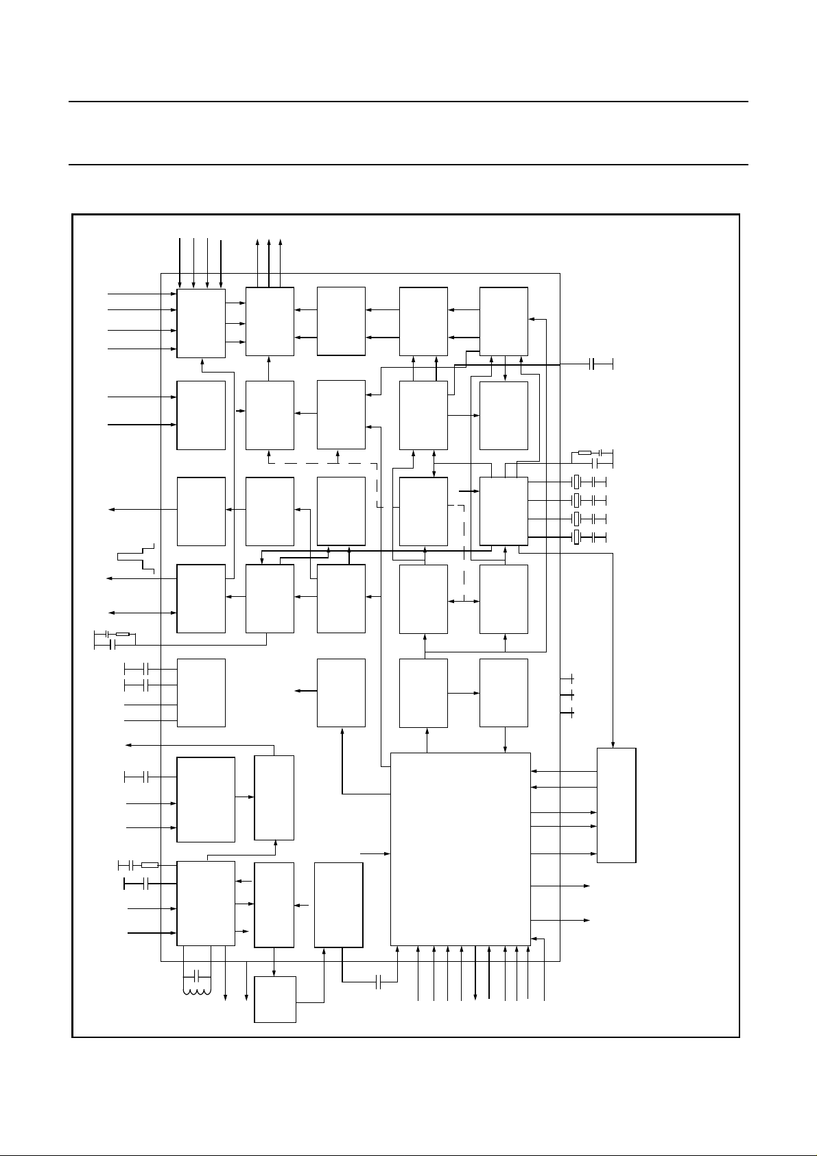
BLOCK DIAGRAM
V
Y
U
V
YU
Y/U/V
Y
Y-DELAY
VERTICAL
SWITCH
Y-DELAY
SYNC
SEPARATOR
UV
BASE-BAND
Y
Y-SWITCH
DELAY LINE
+ TRAPS
VIDEO IDENT
VA
R1 G1 B1 BL1
SDA
SCL
R2G2B2
RGB-MATRIX
C-BUS
2
I
VERTICAL
BL2
TRANSCEIVER
DIVIDER
R-Y B-Y
HELPER
/SECAM
SWITCH
PAL(NTSC)
SECAM
DECODER
SC
F
FILTER
TUNING
HUE
DEMOD.
PAL/NTSC
IDENT
SYSTEM
PLL
PAL/NTSC
HUE CONTR.
TDA 9321H
11-12-96/AC
8V
SIF-IN
VIF-IN
HA/CLP
QSS/AM
PULSE
GENERATOR
SUPPLY
AGC
SIF AMPLIFIER
TOP
AGC/AFC
PLL DEMOD
VIF AMPLIFIER
AFC
SW-OUT
TUNER
VCO+H-PLL
IDENT
QSS MIXER
AM DEMOD.
MUTE
MUTE
VIDEO AMPL.
TRAP
SOUND
SYNC
SEPARATOR
VIDEO IDENT
SWITCH
CORRECTION
GROUP DELAY
Y/CVBS
CONTROL
CVBS INT
FILTER
CLOCHE
ACC
AV-1
CVBS-1
FILTER
BANDPASS
AUTO-
CHROMA
VIDEO SWITCH + CONTROL
AV-2
CVBS-2
SW-OUT
Y(CVBS)-3
C-3
AS
C-4
Y(CVBS)-4
C
Y
SYS2
SYS1
CVBS
SUBCARRIER
Fig.1 BLOCK DIAGRAM TDA 9321H
COMB FILTER
CVBS(PIP)
CVBS(TXT)
June 30, 1998 4
Page 5

Philips Semiconductors Final Device Specification
I2C-bus controlled TV Input Processor
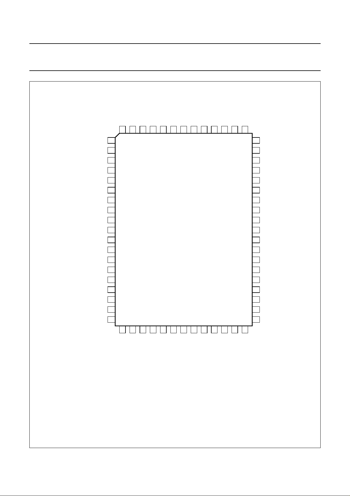
PINNING
SYMBOL PIN DESCRIPTION
AGC
SIF
IFIN1 2 IF input 1
IFIN2 3 IF input 2
AGC
VIF
SIF
/AM
OUT
OUT
PLLIF 6 IF-PLL loop filter
IFVCO1 7 IF VCO tuned circuit 1
IFVCO2 8 IF VCO tuned circuit 2
GND1 9 main ground
IFVO 10 IF video output
V
P1
GDIN 12 group delay correction input
GDOUT 13 group delay correction output
CVBS
INT
AV1 15 AV-1 input
CVBS1 16 CVBS-1 input
AV2 17 AV-2 input
CVBS2 18 CVBS-2 input
SW0 19 output switch (I2C)
CVBS/Y3 20 CVBS/Y-3 input
CHROMA3 21 chrominance-3 input
SW1 22 output switch (I2C)
CVBS/Y4 23 CVBS/Y-4 input
CHROMA4 24 chrominance-4 input
COMBSYS1 25 SYS-1 output for comb filter
COMBCVBS 26 CVBS output for comb filter
COMBSYS2 27 SYS-2 output for comb filter
COMBY 28 luminance input (from comb filter)
COMBC 29 chrominance input (from comb filter)
REFO 30 subcarrier output
GND2 31 digital ground
CVBSO
DEC
CVBSO
DEC
PIP
DIG
TXT
BG
RI1 36 R-1 input
GI1 37 G-1 input
BI1 38 B-1 input
RGBIN1 39 RGB-1 insertion input
RGBIN2 40 RGB-2 insertion input
1 SIF AGC decoupling capacitor
4 VIF AGC decoupling capacitor
5 combined QSS and AM sound output
11 main supply voltage 1 (+8 V)
14 internal CVBS input
32 CVBS (PIP) output
33 digital supply decoupling
34 CVBS (TXT) output
35 bandgap decoupling
TDA 9321H
June 30, 1998 5
Page 6

Philips Semiconductors Final Device Specification
I2C-bus controlled TV Input Processor
SYMBOL PIN DESCRIPTION
RI2 41 R-2 input
GI2 42 G-2 input
BI2 43 B-2 input
GND3 44 ground
V
P2
SCL 46 serial clock input
SDA 47 serial data input/output
AS 48 address select
YO 49 luminance output
UO 50 U-output
VO 51 V-output
DET 52 loop filter burst phase detector
SECPLL 53 SECAM PLL decoupling
XTALA 54 X-tal A (4.433619 MHz)
XTALB 55 X-tal B (3.582056 MHz, PAL-N)
XTALC 56 X-tal C (3.575611 MHz, PAL-M)
XTALD 57 X-tal D (3.579545 MHz, NTSC-M)
PH1LF 58 phase-1 filter
SO 59 sandcastle pulse output
HACLP 60 HA/CLP output/input
VA 61 VA output
AGCOUT 62 tuner AGC output
SIFIN1 63 SIF input 1
SIFIN2 64 SIF input 2
45 positive supply
TDA 9321H
June 30, 1998 6
Page 7
Philips Semiconductors Final Device Specification
I2C-bus controlled TV Input Processor
VA
handbook, full pagewidth
AGCSIF
IFIN1
IFIN2
AGCVIF
SIFO/AMO
PLLIF
IFVCO1
IFVCO2
GND1
IFVO
V
GDIN
GDOUT
CVBS
AV1
CVBS1
AV2
CVBS2
SW0
P1
INT
SIFIN2
64
1
2
3
4
5
6
7
8
9
10
11
12
13
14
15
16
17
18
19
SIFIN1
63
AGCOUT
62
61
HACLP
60
SO
PH1LF
59
58
TDA 9321H
XXX
XTALD
XTALC
57
56
XTALA
XTALB
55
54
SECPLL
DET
53
52
TDA 9321H
VO
51
UO
50
YO
49
48
AS
SDA
47
SCL
46
45
V
P2
44
GND3
43
BI2
GI2
42
41
RI2
RGBIN2
40
RGBIN1
39
BI1
38
37
GI1
RI1
36
DEC
35
34
33
BG
CVBSO
DEC
DIG
TXT
20
21
22
23
24
SW1
CVBS/Y3
CHROMA3
CVBS/Y4
CHROMA4
Fig.2 Pin configuration.
June 30, 1998 7
25
26
27
COMBSYS1
COMBSYS2
COMBCVBS
28
29
COMBY
COMBC
30
REFO
31
GND2
32
MXXxxx
PIP
CVBSO
Page 8

Philips Semiconductors Final Device Specification
I2C-bus controlled TV Input Processor
FUNCTIONAL DESCRIPTION
Vision IF amplifier
The IF-amplifier contains 3 AC-coupled control stages with
a total gain control range which is higher than 66 dB. The
sensitivity of the circuit is comparable with that of modern
IF-IC’s.
The video signal is demodulated by means of a PLL carrier
regenerator. This circuit contains a frequency detector and
a phase detector. During acquisition the frequency
detector will tune the VCO to the right frequency. The initial
adjustment of the oscillator is realised via the I2C-bus. The
switching between SECAM L and L’ can also be realised
via the I2C-bus. After lock-in the phase detector controls
the VCO so that a stable phase relation between the VCO
and the input signal is achieved. The VCO is running at the
double IF frequency. The reference signal for the
demodulator is obtained by means of a frequency divider
circuit. To get a good performance for phase modulated
carrier signals the control speed of the PLL can be
increased by means of the FFI bit.
The AFC output is obtained by using the VCO control
voltage of the PLL and can be read via the I2C-bus. For
fast search tuning systems the window of the AFC can be
increased with a factor 3. The setting is realised with the
AFW bit.
The AGC-detector operates on top sync and top whitelevel. The demodulation polarity is switched via the
I2C-bus. The AGC detector time-constant capacitor is
connected externally. This mainly because of the flexibility
of the application. The time-constant of the AGC system
during positive modulation is rather long to avoid visible
variations of the signal amplitude. To improve the speed of
the AGC system a circuit has been included which detects
whether the AGC detector is activated every frame period.
When during 3 field periods no action is detected the
speed of the system is increased. For signals without peak
white information the system switches automatically to a
gated black level AGC. Because a black level clamp pulse
is required for this way of operation the circuit will only
switch to black level AGC in the internal mode.
The circuit contains a video identification circuit which is
independent of the synchronisation circuit. Therefore
search tuning is possible when the display section of the
receiver is used as a monitor. However, this ident circuit
cannot be made as sensitive as the slower sync ident
circuit (SL) and we recommend to use both ident outputs
to obtain a reliable search system. The ident output is
supplied to the tuning system via the I2C-bus.
TDA 9321H
The input of the identification circuit is connected to pin 14,
the “internal” CVBS input (see Fig.3). This has the
advantage that the ident circuit can also be made
operative when a scrambled signal is received
(descrambler connected between the IF video output (pin
10) and pin 14). A second advantage is that the ident
circuit can be used when the IF amplifier is not used (e.g.
with built-in satellite tuners).
The video ident circuit can also be used to identify the
selected CBVS or Y/C signal. The switching between the
2 modes can be realised with the VIM bit.
The TDA 9321H contains a group delay correction circuit
which can be switched between the BG and a flat group
delay response characteristic. This has the advantage that
in multi-standard receivers no compromise has to be made
for the choice of the SAW filter. Both the input and output
of the group delay correction circuit are externally available
so that the sound trap can be connected between the IF
video output and the group delay correction input. The
output signal of the correction circuit can be supplied to the
video processing circuit and to the SCART plug.
2
The IC has several (I
can be used to switch sound traps or other external
components.
When the IF amplifier is not used the complete IF amplifier
can be switched-off via the I2C-bus by means of the IFO
bit.
Sound circuit
The sound IF amplifier is similar to the vision IF amplifier
and has a gain control range of about 66 dB. The AGC
circuit is related to the SIF carrier levels (average level of
AM or FM carriers) and ensures a constant signal
amplitude of the AM demodulator and the QSS mixer.
The single reference QSS mixer is realised by a multiplier.
In this multiplier the SIF signal is converted to the
intercarrier frequency by mixing it with the regenerated
picture carrier from the VCO. The mixer output signal is
supplied to the output via a high-pass filter for attenuation
of the residual video signals. With this system a high
performance hi-fi stereo sound processing can be
achieved.
The AM sound demodulator is realised by a multiplier. The
modulated sound IF signal is multiplied in phase with the
limited SIF signal. The demodulator output signal is
supplied to the output via a low-pass filter for attenuation
of the carrier harmonics.
C-bus controlled) output ports which
June 30, 1998 8
Page 9
Philips Semiconductors Final Device Specification
I2C-bus controlled TV Input Processor
VIM
IDENT
CVBS
EXT. 2
Y/CVBS
EXT. 3
EXT. 3
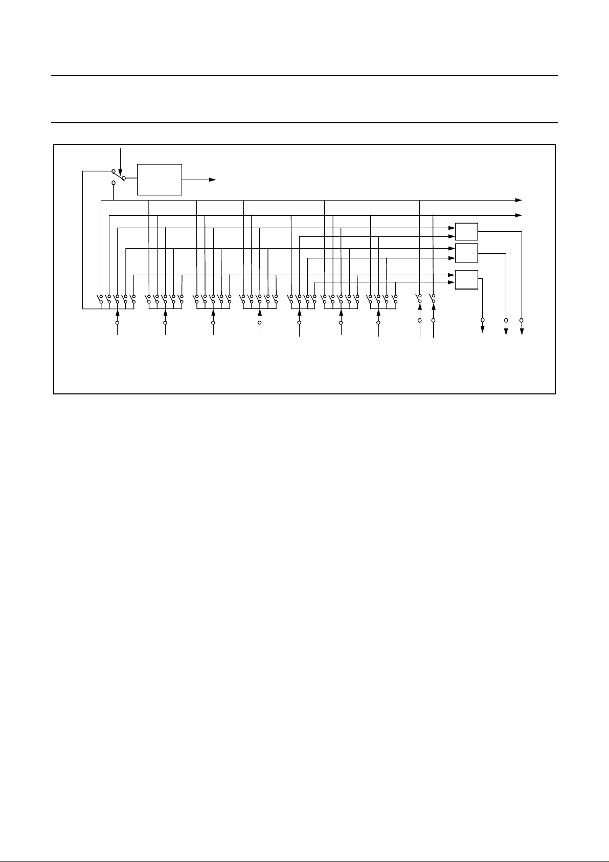
Fig.3 CVBS switch and interfacing of video ident
CVBS-INT
VIDEO
IDENT
CVBS
EXT. 1
TDA 9321H
TO LUMA/SYNC PROCESSING
TO CHROMA PROCESSING
+
+
+
C
Y/CVBS
EXT. 4CEXT. 4
COMB C-IN
COMB Y-IN
CVBS
COMB OUT
TXT
CVBSO
PIP
CVBSO
Video switches
The circuit has 3 CVBS inputs (1 internal and 2 external
inputs) and 2 Y/C inputs. The Y/C inputs can also be used as
additional CVBS inputs. The switch configuration is given in
Fig.3. The selection of the various sources is made via the
I2C-bus.
The circuit can be set in a mode in which it automatically
detects whether a CVBS or a Y/C signal is supplied to the Y/C
inputs. In this mode the TV-standard identification first takes
place on the added Y/CVBS and the C input signal. Then both
chroma input signal amplitudes are checked once and the
input signal with the highest burst signal amplitude is
selected. The result of the detection can be read via the
I2C-bus.
The IC has 2 inputs (AV-1 and AV-2) which can be used to
read the status levels of pin 8 of the SCART plug. The
information is available in the output status byte 02 in the bits
D0-D3.
The 3 outputs of the video switch (CVBSO
, CVBSO
TXT
PIP
and
COMBCVBS) can be independently switched to the various
input signals. The names are just arbitrary and it is for
instance possible to use the COMBCVBS signal to drive the
Comb-filter and the teletext decoder in parallel and to supply
the CVBSO
signal to the SCART plug (via an emitter
TXT
follower).
For comb filter interfacing the circuit has the
COMBCVBS output, a 3rd Y/C input, a reference signal
output (fsc) and 2 control pins which switch the comb
filter to the standard of the incoming signal (as detected
by the ident circuit of the colour decoder). When a signal
is recognised which can be combed and the comb filter
is enabled by the ECMB-bit the Y/C signals coming from
the comb filter are automatically selected. This is
indicated via the CMB-bit in output status byte 02
(D5).For signals which cannot be combed (like SECAM
or Black-to-White signals) the Y/C signals coming from
the comb filter are not selected.
Chroma and luminance processing
The circuits contain a chroma bandpass, the SECAM
cloche filter and chroma trap circuit. The filters are
realised by means of gyrator circuits and they are
automatically calibrated by comparing the tuning
frequency with the X-tal frequency of the decoder. The
luminance delay line is also realised by means of gyrator
circuits. The centre frequency of the chroma bandpass
filter is switchable via the I2C-bus so that the
performance can be optimised for “front-end” signals
and external CVBS signals.
The luminance output signal which is derived from the
incoming CVBS or Y/C signal can be varied in amplitude
by means of a separate gain setting control via the
I2C-bus control bits GAI1 and GAI0. The gain variation
which can be realised with these bits is -1 to +2 dB.
June 30, 1998 9
Page 10

Philips Semiconductors Final Device Specification
I2C-bus controlled TV Input Processor
Colour decoder
The colour decoder can decode PAL, NTSC and SECAM
signals. The PAL/NTSC decoder contains an
alignment-free X-tal oscillator with 4 separate X-tal pins, a
killer circuit and two colour difference demodulators. The
90° phase shift for the reference signal is made internally.
Because it is possible to connect 4 different X-tals to the
colour decoder, all colour standards can be decoded
without external switching circuits. Which X-tals are
connected to the decoder must be indicated via the
I2C-bus. X-tal pins which are not used must be left open.
The horizontal oscillator is calibrated by means of the X-tal
frequency of the colour PLL. For a reliable calibration it is
very important that the X-tal indication bits (XA to XD) are
not corrupted. For this reason the X-tal bits can be read in
the output bytes so that the software can check the I2C
transmission.
The IC’s contain an Automatic Colour Limiting (ACL)
circuit which is switchable via the I2C-bus and which
prevents that oversaturation occurs when signals with a
high chroma-to-burst ratio are received. The ACL circuit is
designed such that it only reduces the chroma signal and
not the burst signal. This has the advantage that the colour
sensitivity is not affected by this function. The ACL function
is mainly intended for NTSC signals and it can also be
used for PAL signals. For SECAM signals the ACL function
should be switched-off.
The SECAM decoder contains an auto-calibrating PLL
demodulator which has two references, viz: the 4.43 MHz
sub-carrier frequency which is obtained from the X-tal
oscillator which is used to tune the PLL to the desired
free-running frequency and the bandgap reference to
obtain the correct absolute value of the output signal. The
VCO of the PLL is calibrated during each vertical blanking
period, when the IC is in search or SECAM mode.
The circuit can also decode the PAL
can insert the various reference signals, set-ups and
timing signals which are required for the PAL
IC’s.
The base-band delay line (TDA 4665 function) is
integrated.
plus
helper signal and
plus
decoder
TDA 9321H
RGB switch and matrix
The IC has 2 RGB inputs with fast switching. The switching
of the various sourcing is controlled via the I2C-bus and the
condition of the switch inputs can be read from the I2C-bus
status bytes. If the RGB signals are not synchronous with
the selected decoder input signal, an external clamp pulse
has to be supplied to the HA/CLP input. The IC must be set
in this mode via the I2C-bus. In that case the VA pulse is
suppressed by switching the VA output in a high
impedance OFF-state.
When an external RGB signal is mixed into the internal
YUV signal it is necessary to switch-off the PAL
demodulation. To detect the presence of a fast blanking a
circuit is added which forces the MACP and HD bit to zero
if a blanking pulse is detected in 2 consecutive lines. This
system is chosen to prevent switching-off at every spike
which is detected on the fast blanking input.
The IC has the possibility to use the RGB1 input as YUV
input. This function can be enabled by means of the YUV
bit in subaddress 0A (D3). When switched to the YUV input
the input signals must have the same amplitude and
polarity as the YUV output signals. The Y signal has to be
supplied to the G1 input, the U signal to the B1 input and
the V signal to the R1 input.
Synchronisation circuit
The sync separator is preceded by a controlled amplifier
which adjusts the sync pulse amplitude to a fixed level.
These pulses are fed to the slicing stage which is operating
at 50% of the amplitude. The separated sync pulses are
fed to the phase detector and to the coincidence detector.
This coincidence detector is used to detect whether the
line oscillator is synchronised and can also be used for
transmitter identification. This circuit can be made less
sensitive by means of the STM bit. This mode can be used
during search tuning to avoid that the tuning system stops
at very weak input signals. The PLL has a very high statical
steepness so that the phase of the picture is independent
of the line frequency.
For the horizontal output pulse 2 conditions are possible,
viz.:
• An HA pulse which has a phase and width which is
identical to the incoming horizontal sync pulse
• A clamp pulse (CLP) which has a phase and width which
is identical to the clamp pulse in the sandcastle pulse
plus
June 30, 1998 10
Page 11

Philips Semiconductors Final Device Specification
I2C-bus controlled TV Input Processor
The HA/CLP signal is generated by means of an oscillator
which is running at a frequency of 440 x fH. Its frequency is
divided by 440 to lock the first loop to the incoming signal.
The time-constant of the loop can be forced by the I2C-bus
(fast or slow). If required the IC can select the
time-constant depending on the noise content of the
incoming video signal.
The free-running frequency of the oscillator is determined
by a digital control circuit which is locked to the reference
signal of the colour decoder. When the IC is switched-on
the HA/CLP is suppressed and the oscillator is calibrated
as soon as all sub-address bytes have been sent. When
the frequency of the oscillator is correct the HA/CLP signal
is switched-on again.
When the coincidence detector indicates an out-of-lock
situation the calibration procedure is repeated.
The VA pulse is obtained via a vertical count down circuit.
The countdown circuit has various windows depending on
the incoming signal (50 Hz or 60 Hz standard or no
standard). The countdown circuit can be forced in various
modes by means of the I2C-bus. To obtain short switching
times of the countdown circuit during a channel change the
divider can be forced in the search window by means of
the NCIN bit.
TDA 9321H
2
C-BUS SPECIFICATION
I
The slave addresses of the IC’s is given in the table below.
The circuit operates up to clock frequencies of 400 kHz.
Slave addresses
A6 A5 A4 A3 A2 A1 A0 R/W
1 0 0 0 1 A1 1 1/0
The bit A1 is controlled via the pin 48 (AS), when the pin is
connected to ground it is a 0 and when connected to the
positive supply line it is a 1. When this pin is left open it is
connected to ground via an internal resistor.
Start-up procedure
Read the status bytes until POR = 0 and send all
subaddress bytes. It is advised to check the bus
transmission by reading the output status bits SXA to SXD.
This ensures a good operation of the calibration system of
the horizontal oscillator. The horizontal output signal is
switched-on when the oscillator is calibrated.
Each time before the data in the IC is refreshed, the status
bytes must be read. If POR = 1, the procedure mentioned
above must be carried out to restart the IC.When this
procedure is not followed the horizontal frequency may be
incorrect after power-up or after a power dip.
Valid subaddresses: 00 to 0E, subaddresses FE and FF
are reserved for test purposes. Auto-increment mode
available for subaddresses.
June 30, 1998 11
Page 12
Philips Semiconductors Final Device Specification
I2C-bus controlled TV Input Processor
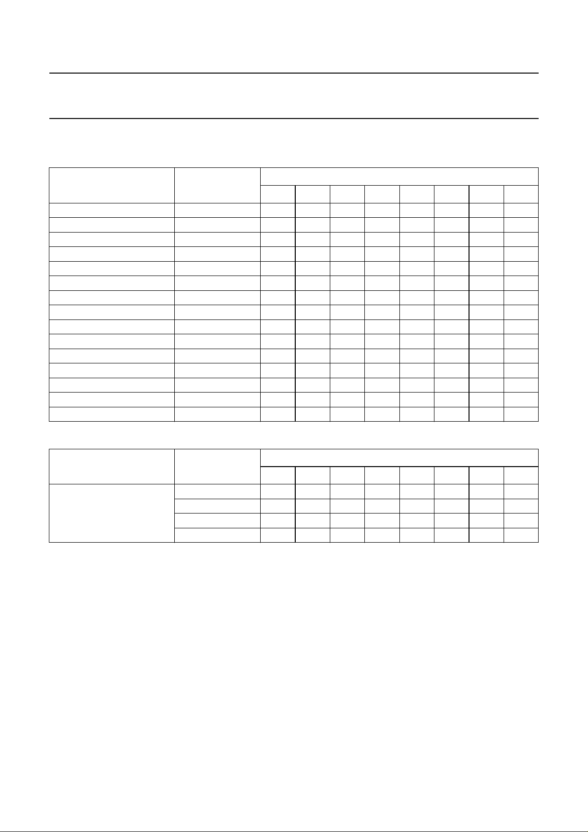
Inputs
Table 1 Input status bits.
FUNCTION
Colour decoder 0 00 CM3 CM2 CM1 CM0 XD XC XB XA
Colour decoder 1 01 MACP HOB HBC HD 0 ACL CB BPS
Luminance 02 0 0 GAI1 GAI0 YD3 YD2 YD1 YD0
Hue control 03 0 0 A5 A4 A3 A2 A1 A0
Spare 04 0 0 000000
Synchronisation 0 05 FORF FORS FOA FOB 0 VIM POC VID
Synchronisation 1 06 0 0 0 0 BSY HO EMG NCIN
Spare 07 0 0 000000
Video switches 0 08 0 0 0 ECMB DEC3 DEC2 DEC1 DEC0
Video switches 1 09 0 PIP2 PIP1 PIP0 0 TXT2 TXT1 TXT0
RGB switch 0A 0 0 0 0 YUV ECL IE2 IE1
Output switches 0B 0 0 0000OS1OS0
Vision IF 0C FFI IFO GD MOD AFW IFS STM VSW
Tuner take-over 0D 0 0 A5 A4 A3 A2 A1 A0
Adjustment IF PLL 0E L’FA A6 A5 A4 A3 A2 A1 A0
SUBADDRESS
(HEX)
D7 D6 D5 D4 D3 D2 D1 D0
DATA BYTE
TDA 9321H
Table 2 Output status bits.
FUNCTION
Output status bytes 00 POR x x x SNR FSI SL IVW
SUBADDRESS
(HEX)
01 CD3 CD2 CD1 CD0 SXD SXC SXB SXA
02 IN1 IN2 CMB YC S2A S2B S1A S1B
03 ID3 ID2 ID1 ID0 IFI PL AFA AFB
D7 D6 D5 D4 D3 D2 D1 D0
DATA BYTE
June 30, 1998 12
Page 13
Philips Semiconductors Final Device Specification
I2C-bus controlled TV Input Processor
INPUT CONTROL BITS
Table 3 Colour decoder mode
CM3 CM2 CM1 CM0 DECODER MODE X-TAL
0 0 0 0 PAL/NTSC/SECAM A
0 0 0 1 PAL/NTSC A
0010PAL A
0 0 1 1 NTSC A
0 1 0 0 SECAM A
0 1 0 1 PAL/NTSC B
0110PAL B
0 1 1 1 NTSC B
1 0 0 0 PAL/NTSC/SECAM ABCD
1 0 0 1 PAL/NTSC C
1010PAL C
1 0 1 1 NTSC C
1 1 0 0 spare
1 1 0 1 PAL/NTSC D
1110PAL D
1 1 1 1 NTSC D
Table 4 X-tal indication
TDA 9321H
Table 6 Helper output blanking (PAL
HOB HBC SNR BLANKING
0--off
10-on
110off
111on
plus
Table 7 PAL
helper demodulation active, note1
HD CONDITION
0off
1 on, PAL
plus
mode with helper set-up 400 mV
and black set-up 200 mV
Note
1. Black and helper set-up will only be present in a norm
sync condition.
Table 8 Automatic colour limiting
ACL COLOUR LIMITING
0 not active
1 active
plus
/EDTV-2)
XA-XD CONDITION
0 X-tal not present
1 X-tal present, note1
Note
1. When a comb filter is used the various X-tals must be
connected to the IC as indicated in the pinning
diagram. This is required because the ident system
switches automatically to the comb filter when a signal
is identified which can be combed (right combination of
colour standard and X-tal frequency). For applications
without comb filter only XA is important (4.43 MHz),
the other pins can then have an arbitrary 3.5 MHz
X-tal.
Table 5 Motion Adaptive Colour Plus, note1
MACP MODE
0 internal 4.43 MHz trap used
1 external MACP chroma filtering used, 4.43
MHz trap bypassed, black set-up 200 mV
Note
1. The black set-up will only be present in a norm sync
condition.
Table 9 Chroma bandpass centre frequency
CB CENTRE FREQUENCY
0F
1 1.1 x F
SC
SC
Table 10 Bypass of chroma base-band delay line
BPS DELAY LINE MODE
0 active
1 bypassed
Table 11 Gain luminance channel
GAI1 GAI0 GAIN SETTING
0 0 -1 dB
0 1 0 dB
1 0 +1 dB
1 1 +2 dB
June 30, 1998 13
Page 14

Philips Semiconductors Final Device Specification
I2C-bus controlled TV Input Processor
Table 12 Y-delay adjustment; note 1
YD0 to YD3 Y-DELAY
YD3 YD3 ∗ 160 ns +
YD2 YD2 ∗ 160 ns +
YD1 YD1 ∗ 80 ns +
YD0 YD0 ∗ 40 ns
Note
1. For an equal delay of the luminance and chrominance
signal the delay must be set at a value of 280 ns
(YD3...YD0 = 1011). This is only valid for a CVBS
signal without group delay distortions.
Table 13 Forced field frequency
FORF FORS FIELD FREQUENCY
0 0 auto (60 Hz when line not
synchronized)
0 1 forced 60 Hz; note 1
1 0 keep last detected field frequency
1 1 auto (50 Hz when line not
synchronized)
Note
1. When switched to this mode the divider will directly
switch to forced 60 Hz only.
Table 14 Phase 1 (ϕ1) time constant, see also table 55
FOA FOB MODE
0 0 normal
0 1 slow
1 0 slow/fast
1 1 fast
Table 15 Video ident mode
VIM MODE
0 ident coupled to internal CVBS (pin 14)
1 ident coupled to selected CVBS
TDA 9321H
Table 16 Synchronization mode
POC MODE
0 active
1 not active
Table 17 Video ident mode
VID VIDEO IDENT MODE
0 ϕ
1 not active
Table 18 Blanked sync on Y
BSY CONDITION
0 unblanked sync, note1
1 blanked sync
Note
1. Except for PAL
Table 19 Condition of horizontal output
HO CONDITION
0 clamp pulse available at H
1HA pulse available at H
Table 20 Enable “Macrovision/subtitle” gating
EMG MODE
0 disable gating
1 enable gating
Table 21 Vertical divider mode
NCIN VERTICAL DIVIDER MODE
0 normal operation
1 switched to search window
loop switched on and off
1
out
plus
with black set-up.
OUT
OUT
June 30, 1998 14
Page 15

Philips Semiconductors Final Device Specification
I2C-bus controlled TV Input Processor
Table 22 Video switch control
ECMB
NOTE 2
0 0 0 0 - INT. CVBS INT. CVBS
0 0 0 1 0 CVBS1 CVBS1
0 0 0 1 1 CVBS2 CVBS2
0 0 1 0 0 CVBS3 CVBS3
0 0 1 0 1 YC3 Y+C3
0 0 1 1 0 CVBS4 CVBS4
0 0 1 1 1 YC4 Y+C4
0 1 1 0 0 AUTO YC3, note1 CVBS3 or Y+C3
0 1 1 1 0 AUTO YC4, note1 CVBS4 or Y+C4
1 0 0 0 - YC COMB INT. CVBS
1 0 0 1 0 YC COMB CVBS1
1 0 0 1 1 YC COMB CVBS2
1 0 1 0 0 YC COMB CVBS3
1 0 1 1 0 YC COMB CVBS4
1 1 1 0 0 AUTO COMB3, note1 CVBS3 or Y+C3
1 1 1 1 0 AUTO COMB4, note1 CVBS4 or Y+C4
DEC3 DEC2 DEC1 DEC0 SELECTED SIGNAL SIGNAL TO COMB
TDA 9321H
Note
1. AUTO YC means the decoder switches between CVBS and YC depending on the presence of the burst signal on
these signals. AUTO COMB means the decoder switches to YC mode if the burst is present on the C input and to
the comb filter output if the burst is present on the CVBS signal.
2. When ECMB = 1 the subcarrier frequency is present at pin 30 (REFO). The Y/C output signals coming from the comb
filter are only switched-on when a signal is received that can be combed.
Table 23 Video switch outputs
TXT2
PIP2
0 0 - INT. CVBS
0 1 0 CVBS1
0 1 1 CVBS2
1 0 0 CVBS3
1 0 1 Y+C3
1 1 0 CVBS4
1 1 1 Y+C4
Table 24 Enable YUV input (on the RGB-1 input)
YUV MODE
TXT1
PIP1
0 RGB-1 input active
1 YUV input active
TXT0
PIP0
OUTPUT SIGNAL TXT
OUTPUT SIGNAL PIP
Table 25 External RGB clamp mode
ECL MODE
0 off, internal clamp pulse used
1 on, external clamp pulse has to be supplied to
the CLP pin
Table 26 Enable fast blanking RGB-1
IE1 FAST BLANKING
0 not active
1 active
Table 27 Enable fast blanking RGB-2
IE2 FAST BLANKING
0 not active
1 active
June 30, 1998 15
Page 16

Philips Semiconductors Final Device Specification
I2C-bus controlled TV Input Processor
Table 28 Output switches (OS1, OS0)
OS0-OS1 CONDITION
0 output is “LOW”
1 output is “HIGH”
Table 29 Fast filter IF-PLL
FFI CONDITION
0 normal time-constant
1 fast time-constant
Table 30 IF circuit not active
IFO MODE
0 normal operation of IF amplifier
1 IF amplifier switched-off
Table 31 Group delay correction
GD GROUP DELAY CHARACTERISTIC
0 flat
1 according to BG standard
TDA 9321H
Table 33 AFC window
AFW AFC WINDOW
0 normal
1 enlarged
Table 34 IF sensitivity
IFS IF SENSITIVITY
0 normal
1 reduced
Table 35 Search tuning mode
STM MODE
0 normal operation
1 reduced sensitivity of video ident circuit
Table 36 Video mute
VSW STATE
0 normal operation
1 IF-video signal switched off
Table 32 Modulation standard
MOD MODULATION
0 negative
1 positive
Table 37 PLL demodulator frequency shift
L’FA MODE
0 normal IF frequency
1 frequency shift for L’ standard
June 30, 1998 16
Page 17

Philips Semiconductors Final Device Specification
I2C-bus controlled TV Input Processor
OUTPUT CONTROL BITS
Table 38 Power-on-reset
POR MODE
0 normal
1 power-down
Table 39 Signal-to-noise ratio of sync signal
SNR SIGNAL-TO-NOISE RATIO
0 S/N > 20 dB
1 S/N < 20 dB
Table 40 Field frequency indication
FSI FREQUENCY
050Hz
160Hz
TDA 9321H
Table 41 Phase 1 (ϕ1) lock indication
SL INDICATION
0 not locked
1 locked
Table 42 Condition vertical divider
IVW STANDARD VIDEO SIGNAL
0 no standard video signal
1 standard video signal in “narrow window” or
standard TV norm (525 or 625 lines)
Table 43 X-tal indication (SXA-SXD)
SXA-SXD CONDITION
0 no X-tal connected
1 X-tal connected
Table 44 Colour decoder mode
CD3 CD2 CD1 CD0 STANDARD X-TAL PIN
0000no colour standard identified A/B/C/D
0001NTSC A
0010PAL A
0011NTSC B
0100PAL B
0101NTSC C
0110PAL C
0111NTSC D
1000PAL D
1001SECAM A
1010illegal forced mode, note 1
Note
1. This output is generated when it is tried to force the decoder to a standard with an X-tal which is not connected to the
IC.
June 30, 1998 17
Page 18

Philips Semiconductors Final Device Specification
I2C-bus controlled TV Input Processor
Table 45 Indication RGB-1/RGB-2 insertion
INX RGB INSERTION
0 no insertion
1 full insertion
Table 46 Condition Y/C input from comb filter
CMB CONDITION Y/C INPUT
0 not selected
1 selected
Table 47 Input signal condition; note 1
YC CONDITION
0 CVBS signal available
1 Y/C signal available
Note
1. During the search mode for the colour system the
YC-bit indicates “1”.
Table 48 Condition of AV-1 and AV-2 input
S1A
S2A
S1B
S2B
0 0 no external source
0 1 external source with 4:3 input signal
1 0 external source with 16:9 input signal
CONDITION
TDA 9321H
Table 50 In-lock indication IF-PLL
PL CONDITION
0 PLL not locked
1 PLL locked
Table 51 AFC output
AFA AFB CONDITION
0 0 outside window; too low
0 1 outside window; too high
1 0 in window; below reference
1 1 in window; above reference
Table 52 IC version indication
ID3 ID2 ID1 ID0 IC TYPE
0001TDA 9321H
0010spare
0011spare
0000spare
0111spare
0100spare
1111spare
1100spare
Table 49 Output video identification
IFI VIDEO SIGNAL
0 no video signal identified
1 video signal identified
June 30, 1998 18
Page 19

Philips Semiconductors Final Device Specification
I2C-bus controlled TV Input Processor
TDA 9321H
LIMITING VALUES
In accordance with the Absolute Maximum Rating System (IEC 134).
SYMBOL PARAMETER CONDITIONS MIN. MAX. UNIT
V
P
T
stg
T
amb
T
sol
T
j
V
es
supply voltage − 9.0 V
storage temperature −25 +150 °C
operating ambient temperature −25 70 °C
soldering temperature for 5 s − 260 °C
operating junction temperature − 150 °C
electrostatic handling HBM; all pins; notes 1 and 2 −3000 +3000 V
MM; all pins; notes 1 and 3 −300 +300 V
Notes
1. All pins are protected against ESD by means of internal clamping diodes.
2. Human Body Model (HBM): R = 1.5 kΩ; C = 100 pF.
3. Machine Model (MM): R = 0 Ω; C = 200 pF.
THERMAL CHARACTERISTICS
SYMBOL PARAMETER VALUE UNIT
R
th j-a
thermal resistance from junction to ambient free air 50 K/W
QUALITY SPECIFICATION
In accordance with
Handbook”
. The handbook can be ordered using the code 9398 510 63011.
“SNW-FQ-611E”
. The number of the quality specification can be found in the
Latch-up
At an ambient temperature of 70 °C all pins meet the following specification:
• I
• I
≥ 100 mA or ≥1.5V
trigger
≤−100 mA or ≤−0.5V
trigger
DD(max)
DD(max)
.
“Quality Reference
June 30, 1998 19
Page 20

Philips Semiconductors Final Device Specification
I2C-bus controlled TV Input Processor
TDA 9321H
CHARACTERISTICS
VP=8V; T
=25°C; unless otherwise specified.
amb
SYMBOL PARAMETER CONDITIONS MIN. TYP. MAX. UNIT
Supplies
UPPLY (PINS 11 AND 45); NOTE 1
S
V
P1
I
P1
P
tot
P
tot
supply voltage 7.2 8.0 8.8 V
supply current − 120 140 mA
total power dissipation − 960 − mW
rise time power supply voltage 10 −−msec
IF circuit
VISION IF AMPLIFIER INPUTS (PINS 2 AND 3)
V
i(rms)
input sensitivity (RMS value) note 2
fi= 38.90 MHz − 35 100 µV
fi= 45.75 MHz − 35 100 µV
fi= 58.75 MHz − 40 100 µV
R
i
C
i
G
cr
V
i max(rms)
input resistance (differential) note 3 − 2 − kΩ
input capacitance (differential) note 3 − 3 − pF
gain control range 70 75 80 dB
maximum input signal
150 200 − mV
(RMS value)
PLL DEMODULATOR (PLL FILTER ON PIN 6); NOTE 4
f
f
t
∆f
FR
CR
AQ
fr
Frequency range PLL 32 − 60 MHz
Catching range PLL 2.0 2.7 3.3 MHz
Acquisition time PLL −− 20 ms
VCO frequency variation with
notes 5 and 6 −− ±20x10-6K
temperature (per °C)
f
R
Tuning range of VCO via
3.0 3.7 4.2 MHz
I2C-bus
∆f Frequency variation per step of
23 29 33 kHz
the DAC (A0-A6)
∆f Frequency shift with the L’FA bit − 5.5 − MHz
-1
June 30, 1998 20
Page 21

Philips Semiconductors Final Device Specification
I2C-bus controlled TV Input Processor
TDA 9321H
SYMBOL PARAMETER CONDITIONS MIN. TYP. MAX. UNIT
VIDEO AMPLIFIER OUTPUT (PIN 10); NOTE 7
V
o
zero signal output level negative modulation;
4.6 4.7 4.8 V
note 8
positive modulation; note 8 1.9 2.0 2.1 V
V
V
∆V
o
o
o
top sync level negative modulation 1.9 2.0 2.1 V
white level positive modulation 4.4 4.5 4.6 V
difference in amplitude between
− 015%
negative and positive
modulation
Z
I
o
bias
video output impedance − 50 −Ω
internal bias current of NPN
1.0 −−mA
emitter follower output transistor
I
source(max)
B bandwidth of demodulated
maximum source current −− 5mA
at −3 dB 6 8 10 MHz
output signal
G
ϕ
NL
V
N
N
diff
diff
vid
th
clamp
ins
differential gain note 9 −− 1.5 %
differential phase notes 9 and 6 −− 2.5 deg
video non-linearity note 10 − 2.5 5 %
white spot clamp level − 6.0 − V
noise inverter clamping level note 11 − 1.5 − V
noise inverter insertion level
note 11 − 2.7 − V
(identical to black level)
δ
mod
intermodulation notes 6 and 12
blue Vo= 0.92 or 1.1 MHz 60 66 − dB
Vo= 2.66 or 3.3 MHz 60 66 − dB
yellow Vo= 0.92 or 1.1 MHz 56 62 − dB
Vo= 2.66 or 3.3 MHz 60 66 − dB
S/N signal-to-noise ratio notes 6 and 13
weighted 56 60 65 dB
unweighted 49 53 − dB
V
o
V
o
residual carrier signal note 6 − 5.5 − mV
residual 2nd harmonic of carrier
note 6 − 2.5 − mV
signal
supply ripple reduction at the
− 40 − dB
output
June 30, 1998 21
Page 22

Philips Semiconductors Final Device Specification
I2C-bus controlled TV Input Processor
TDA 9321H
SYMBOL PARAMETER CONDITIONS MIN. TYP. MAX. UNIT
IF AND TUNER AGC; NOTE 14
Timing of IF-AGC with a 2.2µF capacitor (pin 4)
modulated video interference 60% AM for 1 mV to
−− 10 %
100 mV; 0 to 200 Hz
(system B/G)
t
inc
t
dec
I
L
∆V
o
response time to IF input signal
amplitude increase of 52 dB
response to an IF input signal
amplitude decrease of 52 dB
allowed leakage current of the
AGC capacitor
change in video output signal
amplitude over 1 vertical period
positive and negative
− 2 − ms
modulation
negative modulation − 50 − ms
positive modulation − 100 − ms
negative modulation −− 10 µA
positive modulation −− 200 nA
for AGC capacitor with a
−− 2%
value of 0.5 µF
for peak white AGC at positive
modulation
Tuner take-over adjustment (via I2C-bus)
V
i(rms)
minimum starting level for tuner
− 0.4 0.8 mV
take-over (RMS value)
V
i(rms)
maximum starting level for tuner
100 150 − mV
take-over (RMS value)
Maximum variation of take-over
point with temperature (T
amb
− 68dB
between 0 and 70 °C)
Tuner control output (pin 62)
V
V
omax
o(sat)
maximum tuner AGC output
voltage
maximum tuner gain;
note 3
output saturation voltage minimum tuner gain;
−− 9V
−− 300 mV
IO=2mA
I
omax
maximum tuner AGC output
5 −−mA
swing
I
L
∆V
i
leakage current RF AGC −− 1 µA
input signal variation for
0.5 2 4 dB
complete tuner control
AFC OUTPUT (VIA I2C-BUS); NOTE 15
RES AFC resolution − 2 − bits
W
W
sen
senL
window sensitivity 65 80 100 kHz
window sensitivity in large
195 240 300 kHz
window mode
VIDEO IDENTIFICATION OUTPUT (VIA I2C-BUS)
t
d
delay time of identification after
−− 10 ms
the AGC has stabilized on a
new transmitter
June 30, 1998 22
Page 23

Philips Semiconductors Final Device Specification
I2C-bus controlled TV Input Processor
TDA 9321H
SYMBOL PARAMETER CONDITIONS MIN. TYP. MAX. UNIT
Sound IF circuit
SOUND IF AMPLIFIER (PINS 63 AND 64)
V
i(rms)
input sensitivity (RMS value)
FM mode (-3 dB) − 30 70 µV
AM mode (-3 dB) − 70 100 µV
V
i max(rms)
maximum input signal
(RMS value)
FM mode 50 70 − mV
AM mode 80 140 − mV
R
i
C
i
G
cr
input resistance (differential) note 3 − 2 − kΩ
input capacitance (differential) note 3 − 3 − pF
gain control range 64 −−dB
crosstalk between SIF and VIF
50 −−dB
input
QSS AND AM SOUND OUTPUT (PIN 5)
General
R
V
I
o
o
bias
output resistance −− 250 Ω
DC output voltage − 3.3 − V
internal bias current of emitter
0.7 1.0 − mA
follower
I
o
maximum AC and DC sink
− 0.7 − mA
current
I
o
maximum AC and DC source
− 2.0 − mA
current
QSS output signal
V
o(rms)
output signal amplitude (RMS
SC-1; sound carrier 2 off 75 100 125 mV
value)
B bandwidth (-3 dB) 7.5 9 − MHz
V
o(rms)
residual IF sound carrier (RMS
− 2 − mV
value)
S/N weighted S/N ratio (SC1/SC2).
Ratio of PC/SC1 at vision IF
input of 40 dB or higher, note 16
black picture 53/48 58/55 − dB
white picture 52/47 55/53 − dB
6 kHz sinewave
44/42 48/46 − dB
(black-to-white modulation)
250 kHz sine wave
44/25 48/30 − dB
(black-to-white modulation)
sound carrier
45/44 51/50 − dB
subharmonics (f=2.75 MHz
± 3 kHz)
sound carrier
46/45 52/51 − dB
subharmonics (f=2.87 MHz
3 kHz)
June 30, 1998 23
Page 24

Philips Semiconductors Final Device Specification
I2C-bus controlled TV Input Processor
SYMBOL PARAMETER CONDITIONS MIN. TYP. MAX. UNIT
AM output signal
V
o(rms)
THD total harmonic distortion − 0.5 1.0 %
B AF bandwidth −3 dB 100 125 − kHz
S/N weighted signal-to-noise ratio 47 53 − dB
AF output signal amplitude
(RMS value)
54% modulation 400 500 600 mV
TDA 9321H
June 30, 1998 24
Page 25

Philips Semiconductors Final Device Specification
I2C-bus controlled TV Input Processor
TDA 9321H
SYMBOL PARAMETER CONDITIONS MIN. TYP. MAX. UNIT
CVBS AND Y/C INPUTS/OUTPUTS AND COMB FILTER INTERFACE
CVBS-Y/C SWITCH
V
i(p-p)
CVBS or Y input voltage
note 17 − 1.0 1.43 V
(peak-to-peak value)
I
i
Z
SS
s
CVBS
CVBS or Y input current − 4 −µA
maximum source impedance −− 1.0 kΩ
suppression of non-selected
f = 0 to 5 MHz, note 6 50 −−dB
CVBS input signal
V
i
chrominance input voltage
note 3 and 18 − 0.3 1.0 V
(burst amplitude)
Z
V
V
V
V
V
V
Z
i
o(p-p)
oBL
oBL
o(p-p)
oBL
oBL
o
chrominance input impedance − 50 − kΩ
output signal amplitude
(CVBS
black level of CVBS
) (peak-to-peak value)
TXT
TXT
temperature dependence of
black level of CVBS
TXT
output signal amplitude
(CVBS
black level of CVBS
) (peak-to-peak value)
PIP
PIP
temperature dependence of
black level of CVBS
PIP
1.6 2.0 2.4 V
− 2.6 − V
− +4 − mV/K
0.8 1.0 1.2 V
− 3.6 − V
− +9 − mV/K
output impedance −− 250 Ω
COMB FILTER INTERFACE, NOTE19
V
o(p-p)
CVBS output signal amplitude
0.8 1.0 1.2 V
(peak-to-peak value)
Z
o
V
oBL
V
oBL
output impedance −− 250 Ω
black level at output − 3.6 − V
temperature dependence of
− +9 − mV/K
black level
V
i(p-p)
Y input voltage (peak-to-peak
− 1.0 1.43 V
value)
I
i
V
i
Y input current − 4 −µA
chrominance input voltage
− 0.3 1.0 V
(burst amplitude)
Z
i
chrominance input impedance − 50 − kΩ
Reference signal output, note
V
o(p-p)
output signal amplitude
(C
=15 pF) (peak-to-peak
LOAD
20
value)
V
o
V
o
output level to enable comb filter 4.0 4.2 4.6 V
output level to disable comb
filter
June 30, 1998 25
0.2 0.25 0.3 V
− 0.1 1.4 V
Page 26

Philips Semiconductors Final Device Specification
I2C-bus controlled TV Input Processor
TDA 9321H
SYMBOL PARAMETER CONDITIONS MIN. TYP. MAX. UNIT
Switching levels of SYS1/SYS2 outputs, note
V
o
V
o
I
o
I
o
output level HIGH 4.0 5.0 5.5 V
output level LOW − 0.1 0.4 V
sink current 2 −−mA
source current 2 −−mA
21
DETECTION OF STATUS LEVELS OF PIN 8 OF SCART PLUG, NOTE 22
V
i
detection between “internal” and
2.0 2.2 2.4 V
“external(16:9)” source
V
i
detection between “external
5.3 5.5 5.7 V
(16:9)” and “external (4:3)”
source
R
i
input resistance 60 100 − kΩ
Chrominance/Luminance filters and delay lines
CHROMINANCE TRAP CIRCUIT; NOTE 23
f
trap
ftrap trap frequency during SECAM
trap frequency f
± 1% MHz
osc
4.3 ± 1.5% MHz
reception
B Bandwidth at fSC = 3.58 MHz −3 dB 2.6 2.8 3.0 MHz
B Bandwidth at fSC = 4.43 MHz −3 dB 3.2 3.4 3.6 MHz
B Bandwidth during SECAM
−3 dB 2.9 3.1 3.3 MHz
reception
SR colour subcarrier rejection 26 −−dB
CHROMINANCE BANDPASS CIRCUIT
f
c
f
c
centre frequency (CB = 0) − f
osc
centre frequency (CB = 1) − 1.1xf
osc
− MHz
− MHz
QBP bandpass quality factor − 3 −
CLOCHE FILTER
f
c
centre frequency 4.26 4.29 4.31 MHz
B Bandwidth 241 268 295 kHz
Y DELAY LINE
t
d
delay time YD3...YD0 = 1011; Xtal: A;
490 520 550 ns
note 6
t
d
delay time YD3...YD0 = 1011; Xtal: B,
530 560 590 ns
C or D; note 6
t
d1
tuning range delay time with respect to 520/560 ns,
−280 − +160 ns
12 settings, see Table 12
B bandwidth of internal delay line note 6 8 −−MHz
June 30, 1998 26
Page 27

Philips Semiconductors Final Device Specification
I2C-bus controlled TV Input Processor
TDA 9321H
SYMBOL PARAMETER CONDITIONS MIN. TYP. MAX. UNIT
GROUP DELAY CORRECTION, NOTE 24
V
i(p-p)
input signal amplitude
− 2.0 − V
(peak-to-peak value)
I
i
V
o(p-p)
input current − 0.1 1.0 µA
output signal amplitude
1.8 2.0 2.2 V
(peak-to-peak value)
Z
o
V
o
V
oBL
output impedance −− 250 Ω
top sync level at output − 2.4 − V
temperature dependence of top
− +5 − mV/K
sync level
Colour demodulation part
CHROMINANCE AMPLIFIER
ACC
cr
∆V change in amplitude of the
ACC control range note 25 26 −−dB
−− 2dB
output signals over the ACC
range
THR
on
threshold colour killer from colour OFF to colourON−34 −−30 dB
HYS
off
hysteresis colour killer strong signal conditions;
ACL CIRCUIT; NOTE 26
chrominance burst ratio at
which the ACL starts to operate
REFERENCE PART
Phase-locked loop; note
f
CR
catching range ±360 ±600 − Hz
27
∆ϕ phase shift for a ±400 Hz
deviation of the oscillator
frequency
Oscillator
TC
osc
temperature coefficient of the
oscillator frequency
f
osc
oscillator frequency deviation
with respect to the supply
R
i
C
i
minimum negative resistance −− 1.0 kΩ
maximum load capacitance −− 15 pF
HUE CONTROL
HUE
cr
∆HUE hue variation for ±10% V
hue control range 63 steps; see Fig.4 ±35 ±40 − deg
P
∆HUE/∆T hue variation with temperature T
− +3 − dB
S/N ≥ 40 dB; note 6
noisy input signals; note 6 − +1 − dB
− 3.0 −
note 6 −− 2 deg
note 6 −− 1 Hz/K
note 6; VP=8V±10% −− 25 Hz
note 6 − 0 − deg
=0to70°C; note 6 − 0 − deg
amb
June 30, 1998 27
Page 28

Philips Semiconductors Final Device Specification
I2C-bus controlled TV Input Processor
TDA 9321H
SYMBOL PARAMETER CONDITIONS MIN. TYP. MAX. UNIT
DEMODULATORS
General
∆V spread of signal amplitude ratio
note 6 −1 − +1 dB
between standards
PAL/NTSC demodulator
G gain between both
1.60 1.78 1.96
demodulators G(B−Y) and
G(R−Y)
B bandwidth of demodulators −3 dB; note 29 − 650 − kHz
PAL/NTSC demodulator (continued)
V
V
o(p-p)
o(p-p)
residual carrier output
(peak-to-peak value)
H/2 ripple at (R−Y) output
f=f
; (R−Y) output 5 mV
osc
f=f
; (B−Y) output −− 5mV
osc
f=2f
f=2f
; (R−Y) output 5 mV
osc
; (B−Y) output −− 5mV
osc
−− 25 mV
(peak-to-peak value)
∆Vo/∆T change of output signal
note 6 − 0.1 − %/K
amplitude with temperature
∆Vo/∆V
P
change of output signal
note 6 −− 0.3 dB/V
amplitude with supply voltage
ϕ
e
phase error in the demodulated
note 6 −− ±5 deg
signals
SECAM demodulator
∆f
BL
black level off-set −− 7 kHz
TC
BL
temperature dependence of
−− 60 Hz/K
black level
fP pole frequency of deemphasis 77 85 93 kHz
ratio pole and zero frequency − 3 −
NL non linearity −− 3%
VCAL calibration voltage 3 4 5 V
June 30, 1998 28
Page 29

Philips Semiconductors Final Device Specification
I2C-bus controlled TV Input Processor
TDA 9321H
SYMBOL PARAMETER CONDITIONS MIN. TYP. MAX. UNIT
Base-band delay line
∆V
o
variation of output signal for
−0.1 − 0.1 dB
adjacent time samples at
constant input signals
V
o(p-p)
residual clock signal
−− 5mV
(peak-to-peak value)
t
D
t
D
∆V
o
delay of delayed signal 63.94 64.0 64.06 µs
delay of non-delayed signal 40 60 80 ns
difference in output amplitude
−− 5%
when delay line is bypassed or
not (via BPS-bit)
plus
PAL
V
helper demodulator
o(p-p)
helper output voltage
610 686 770 mV
(peak-to-peak value)
∆V
t
D
o
helper set-up amplitude only helper lines 22 and 23 380 400 420 mV
group delay within passband −− 10 ns
∆ϕ demodulation phase error including H/2 phase error −− 5 deg.
SS
helper
suppression of modulated
−36 −−dB
helper in demodulated signal
(0-1 MHz)
residual 4.43 MHz signal −36 −−dB
harmonic distortion in ACC −36 −−dB
∆t helper output timing to Y output −− 10 ns
∆V
o
off-set demodulated mid grey to
−− 5mV
inserted mid grey level (mid
grey line 23 - line 22)
t helper set-up width − 52.8 −µs
t delay between mid sync of input
note 30 − 8.6 −µs
and start of helper set-up
(YD3...YD0=1011)
t delay between start black set-up
− 30.8 −µs
and start helper set-up (only line
22 and 23)
B base-band helper bandwidth −3 dB − 2.6 − MHz
June 30, 1998 29
Page 30

Philips Semiconductors Final Device Specification
I2C-bus controlled TV Input Processor
TDA 9321H
SYMBOL PARAMETER CONDITIONS MIN. TYP. MAX. UNIT
RGB/YUV switch and YUV outputs
RGB INPUTS
V
i(p-p)
input signal amplitude
− 0.7 1.0 V
(peak-to-peak value)
Z
∆V
s
o
maximum source impedance −− 1.0 kΩ
difference between black level of
−− 10 mV
internal and external signals at
the outputs
I
∆t
i
d
input currents no clamping; note 3 − 0.1 1 µA
delay difference for the three
note 6 − 020ns
channels
YUV INPUTS (WHEN ACTIVATED)
V
i(p-p)
Y input signal amplitude
− 1.0 − V
(peak-to-peak value)
V
i(p-p)
U/V input signal amplitude
− 1.33/1.05 − V
(peak-to-peak value)
Z
∆V
s
o
maximum source impedance −− 1.0 kΩ
difference between black level
−− 10 mV
of internal and external signals
at the outputs
I
i
input currents no clamping; note 3 − 0.1 1 µA
FAST BLANKING
V
i
input voltage no data insertion −− 0.4 V
data insertion 0.9 −−V
V
∆t
i(max)
d
maximum input pulse −− 3.5 V
delay difference of blanking and
note 6 −− tbf ns
RGB signals
I
i
SS
SS
t
D
int
ext
input current −− 0.2 mA
suppression of internal YUV
signals
suppression of external RGB
signals
delay between blanking input
notes 6; insertion;
fi= 0 to 5 MHz
notes 6; no insertion;
fi= 0 to 5 MHz
55 −−dB
55 −−dB
−− tbf ns
and YUV outputs
June 30, 1998 30
Page 31

Philips Semiconductors Final Device Specification
I2C-bus controlled TV Input Processor
TDA 9321H
SYMBOL PARAMETER CONDITIONS MIN. TYP. MAX. UNIT
Y OUTPUT, NOTE 31
V
o(p-p)
output signal amplitude
black-to-white − 1.0 − V
(peak-to-peak value)
V
∆V
o(p-p)
o
output voltage during PAL
difference in black level between
plus
black-to-white − 0.8 − V
−− 10 mV
YUV and RGB mode
Z
o
V
o
B bandwidth of the RGB switch
output impedance −− 250 Ω
output DC level black level 2.8 3.0 3.2 V
7 −−MHz
circuit (−3 dB)
S/N signal-to-noise ratio f = 0 - 5 MHz − 52 − dB
V
o
black set-up amplitude MACP=1 or HD=1 190 200 210 mV
black set-up width − 52.8 −µs
∆t delay between mid-sync at input
note 30 − 8.8 −µs
and black set-up
∆V
o
off-set Y
to re-inserted
BLACK
−− 10 mV
black
G gain from Y/CVBSIN to Y
G gain from Y/CVBSIN to Y
OUT
OUT
MACP = 1 or HD = 1 1.08 1.14 1.20
1.35 1.43 1.50
UV OUTPUTS
V
o(p-p)
output voltage V (peak-to-peak
standard EBU colour bar 0.88 1.05 1.25 V
value)
V
o(p-p)
output voltage U (peak-to-peak
standard EBU colour bar 1.12 1.33 1.58 V
value)
Z
V
∆V
o
o
o
output impedance −− 250 Ω
output DC level 2.2 2.4 2.6 V
difference in black level between
−− 10 mV
YUV and RGB mode
COLOUR MATRIX FROM RGB TO YUV
G gain from R to Y
G gain from G to Y
G gain from B to Y
G gain from R to U
G gain from G to U
G gain from B to U
G gain from R to V
G gain from G to V
G gain from B to V
OUT
OUT
OUT
OUT
OUT
OUT
OUT
OUT
OUT
0.40 0.43 0.46
0.79 0.84 0.90
0.15 0.16 0.17
0.40 0.43 0.46
0.79 0.84 0.90
1.19 1.27 1.35
0.94 1.00 1.07
0.79 0.84 0.90
0.15 0.16 0.17
June 30, 1998 31
Page 32

Philips Semiconductors Final Device Specification
I2C-bus controlled TV Input Processor
TDA 9321H
SYMBOL PARAMETER CONDITIONS MIN. TYP. MAX. UNIT
Horizontal and vertical synchronization
SYNC VIDEO INPUTS
V
SL
SL
i
HS
VS
sync pulse amplitude note 3 35 300 350 mV
slicing level for horizontal sync note 32 45 50 55 %
slicing level for vertical sync note 32 27 30 33 %
HORIZONTAL OSCILLATOR
f
∆f
fr
fr
free running frequency − 15625 − Hz
spread on free running
−− ±2%
frequency
∆f/∆V
P
frequency variation with respect
VP= 8.0 V ±10%; note 6 − 0.2 0.5 %
to the supply voltage
∆f
(max)
frequency variation with
T
=0to70°C; note 6 −− 80 Hz
amb
temperature
FIRST CONTROL LOOP; NOTE 33
f
HR
f
CR
S/N signal-to-noise ratio of the
holding range PLL −±0.9 ±1.2 kHz
catching range PLL note 6 ±0.6 ±0.9 − kHz
18 20 22 dB
video input signal at which the
time constant is switched
HYS hysteresis at the switching point 2 3 4 dB
jitter (± 3σ) when in automatic
−− 5ns
mode
H
OUTPUT AND CLP OUTPUT/INPUT
A
Switched to HA output (HO = 1)
V
o
V
o
I
o
I
o
t pulse width at nominal horizontal
output voltage HIGH at a source current of 2 mA 4.0 5.0 5.5 V
output voltage LOW at a sink current of 2 mA − 0.2 0.4 V
sink current 2 −−mA
source current 2 −−mA
4.6 4.7 4.8 µs
frequency
∆t delay between mid sync of input
note 30 0.3 0.45 0.6 µs
and mid HA pulse
Switched to CLP output (HO = 0)
t CLP pulse width at nominal horizontal
3.5 3.6 3.7 µs
frequency
∆t delay between start CLP pulse
to start black set-up
HD=1 or MACP=1,
YD3...YD0=1011, and
5.2 5.3 5.4 µs
nominal horizontal
frequency
∆t delay between mid sync of input
note 30 3.0 3.2 3.4 µs
and start CLP
June 30, 1998 32
Page 33

Philips Semiconductors Final Device Specification
I2C-bus controlled TV Input Processor
TDA 9321H
SYMBOL PARAMETER CONDITIONS MIN. TYP. MAX. UNIT
Switched to CLP input (ECL=1)
V
i
V
i
input voltage LOW 0 − 0.6 V
input voltage HIGH 2.4 − 5.5 V
Switched to CLP input (ECL=1) (continued)
t clamping pulse width 1.8 3.5 −µs
∆V
Z
o
i
clamping off-set on UV outputs −− 10 mV
input impedance 3 −−MΩ
VERTICAL OSCILLATOR; NOTE 34
f
f
fr
lock
free running frequency − 50/60 − Hz
locking range 45 − 64.5 Hz
divider value not locked − 625/525 − lines
locking range 488 − 722 lines/
frame
V
OUTPUT
A
V
o
V
o
I
o
I
o
output voltage HIGH at a source current of 2 mA 4.0 5.0 5.5 V
output voltage LOW at a sink current of 2 mA − 0.2 0.4 V
sink current 2 −−mA
source current 2 −−mA
t pulse width fV = 50 Hz − 2.5 − lines
t pulse width fV = 60 Hz − 3.0 − lines
∆t delay between start of vertical
note 35 − 37.7 −µs
sync of input and positive edge
of V
A
Z
o
output impedance ECL = 1 3 −−MΩ
SANDCASTLE OUTPUT
General
V
o
I
o
zero level 0 0.5 1.0 V
sink current − 0.7 − mA
Horizontal/vertical blanking
V
o
I
o
voltage level 2.2 2.5 2.8 V
source current − 0.7 − mA
t horizontal blanking width − 10 −µs
∆t delay between start horizontal
− 6.4 −µs
blanking and start clamping
pulse
June 30, 1998 33
Page 34

Philips Semiconductors Final Device Specification
I2C-bus controlled TV Input Processor
TDA 9321H
SYMBOL PARAMETER CONDITIONS MIN. TYP. MAX. UNIT
Clamping pulse
V
o
I
o
voltage level 4.2 4.5 4.8 V
source current − 0.7 − mA
t pulse width − 3.6 −µs
∆t delay between mid sync of input
note 30 3.0 3.2 3.4 µs
and start of clamping pulse
2
C-BUS CONTROL INPUTS/OUTPUTS
I
SDA/SCL INPUTS/OUTPUTS
V
i
V
i
V
i
I
i
I
i
V
o
input voltage level 0 − 5.5 V
low-level input voltage −− 1.5 V
high-level input voltage 3.5 −−V
low-level input current Vi = 0 V −− -10 µA
high-level input current Vi = 5.5 V −− 10 µA
low-level output voltage SDA, IL = 3 mA −− 0.4 V
GENERAL PURPOSE SWITCH OUTPUTS, NOTE 36
V
o
V
o
I
o
I
o
output voltage HIGH 4.0 5.0 5.5 V
output voltage LOW − 0.2 0.4 V
sink current 2 −−mA
source current 2 −−mA
Notes
1. The 2 supply pins must be decoupled separately but they must be derived from the same main supply to avoid too
big differences between the two.
2. On set AGC.
3. This parameter is not tested during production and is just given as application information for the designer of the
television receiver.
4. Loop bandwidth BL = 60 kHz (natural frequency fN = 15 kHz; damping factor d = 2; calculated with top sync level as
FPLL input signal level). LC-VCO circuit: Q0 = 60, C
= 30 pF.
int.
5. The optimum temperature stability of the PLL can be obtained when a Toko coil as given in Table 53 is applied.
6. This parameter is not tested during production but is guaranteed by the design and qualified by means of matrix
batches which are made in the pilot production period.
7. Measured at 10 mV (RMS) top sync input signal.
8. So called projected zero point, i.e. with switched demodulator.
9. Measured in accordance with the test line given in Fig.5. For the differential phase test the peak white setting is
reduced to 87%.
The differential gain is expressed as a percentage of the difference in peak amplitudes between the largest and
smallest value relative to the subcarrier amplitude at blanking level.
The phase difference is defined as the difference in degrees between the largest and smallest phase angle.
10. This figure is valid for the complete video signal amplitude (peak white-to-black), see Fig.6.
11. The noise inverter is only active in the “strong signal mode” (no noise detected in the incoming signal)
12. The test set-up and input conditions are given in Fig.7. The figures are measured with an input signal of 10 mV RMS.
June 30, 1998 34
Page 35

Philips Semiconductors Final Device Specification
I2C-bus controlled TV Input Processor
13. Measured at an input signal of 10 mV
voltage (RMS value). B = 5 MHz. Weighted in accordance with CCIR 567.
14. The AGC response time is also dependent on the acquisition time of the PLL demodulator. The values given are valid
when the PLL is in lock.
15. The AFC control voltage is obtained from the control voltage of the VCO of the PLL demodulator. The tuning
information is supplied to the tuning system via the I2C-bus. 2 bits are reserved for this function. The AFC value is
valid only when the PL-bit is 1.
16. The weighted S/N ratio is measured under the following conditions:
a) The vision IF modulator must meet the following specifications:
Incidental phase modulation for black-to-white jumps less than 0.5 degrees.
QSS AF performance, measured with the television-demodulator AMF2 (audio output, weighted S/N ratio) better
than 60 dB (deviation 27 kHz) for 6 kHz sine wave black-to-white modulation.
Picture-to-sound carrier ratio: PC/SC1 = 13 dB (transmitter).
b) The measurements must be carried out with the Siemens SAW filters G3962 for vision IF and G9350 for sound
IF. Input level for sound IF 10 mV
c) The PC/SC ratio at the vision IF input is calculated as the addition of the TV transmitter ratio and the SAW filter
PC/SC ratio. This PC/SC ratio is necessary to achieve the S/N(W) values as indicated.
17. Signal with negative-going sync. Amplitude includes sync pulse amplitude.
18. Indicated is a signal for a colour bar with 75% saturation (chroma : burst ratio = 2.2 : 1).
19. When a signal is identified which can be combed (right combination of colour standard and reference X-tal) the comb
filter is switched to that mode via the SYS1 and SYS2 pins and then the filter is activated by switching on the
reference carrier signal and connecting the Y/C output signal of the comb filter to the video processing circuits.
20. The subcarrier output signal can be used as reference signal for external comb filter IC’s (e.g. SAA 4961). When the
ECMB bit is low the subcarrier signal is suppressed and the dc level is low. With the ECMB bit high the output level
is high and the subcarrier signal is present.
21. The outputs SYS1 and SYS2 can be used to switch the comb filter to the different colour standards like PAL-M,
PAL-N, PAL-B,G and NTSC-M and are controlled by the colour decoder identification circuit.
The setting of the outputs for the various standards is given in table 54.
22. For the detection of the status of the incoming SCART signal a voltage divider with a ratio of 2/3 has to be connected
between pin 8 of the SCART plug and the detection input. The impedance of the voltage divider should not be too
high-ohmic because of the input impedance of 100 kΩ.
23. When the decoder is forced to a fixed subcarrier frequency (via the XA-XD or the CM-bits) the chroma trap is always
switched-on, also when no colour signal is identified. When 2 X-tals are active the chroma trap is switched-off when
no colour signal is identified.
24. The typical group delay characteristic for the BG standard is given in Fig.8.
25. At a chrominance input voltage of 660 mV (p-p) (colour bar with 75% saturation i.e. burst signal amplitude
300 mV (p-p)) the dynamic range of the ACC is +6 and −20 dB.
26. The ACL function can be activated by via the ACL bit. The ACL circuit reduces the gain of the chroma amplifier for
input signals with a chroma-to-burst ratio which exceeds a value of 3.0.
. The S/N is the ratio of black-to-white amplitude to the black level noise
RMS
with 27 kHz deviation.
RMS
TDA 9321H
June 30, 1998 35
Page 36

Philips Semiconductors Final Device Specification
I2C-bus controlled TV Input Processor
27. All frequency variations are referenced to 3.58 or 4.43 MHz carrier frequency.
All oscillator specifications are measured with the Philips crystal series 9922 520 with a series capacitance of 18 pF.
The oscillator circuit is rather insensitive to the spurious responses of the X-tal. As long as the resonance resistance
of the third overtone is higher than that of the fundamental frequency the oscillator will operate at the right frequency.
The typical crystal parameters for the X-tals mentioned above are:
a) Load resonance frequency f0= 4.433619, 3.579545, 3.582056 and 3.575611 MHz; CL= 20 pF.
b) Motional capacitance CM= 20.6 fF (4.43 MHz crystal) or 14.7 fF (3.58 MHz crystal).
c) Parallel capacitance C0= 5.0 pf.
The minimum detuning range can only be specified if both the IC and the X-tal tolerances are known and therefore
the figures regarding catching range are only valid for the specified X-tal series. In this figure tolerances of the X-tal
with respect to the nominal frequency, motional capacitance and ageing have been taken into account and have
been counted for by gaussic addition.
Whenever different typical X-tal parameters are used the following equation might be helpful for calculating the
impact on the tuning capabilities:
Detuning range = CM /(1 + C0/CL)
The resulting detuning range should be corrected for temperature shift and supply voltage deviation of both the IC
and the X-tal. To guarantee a catching range of ±300 Hz on 4.43 MHz the minimum motional capacitance of the X-tal
must have a value 13.2 fF or higher. For a catching range of 250 Hz with the 3.58 MHz X-tal the minimum motional
capacitance must have a value of 9 fF.
The actual series capacitance in the application should be CL = 18 pF to account for parasitic capacitances on and
off chip.
28. The hue control is active for NTSC on the demodulated colour difference signals and for PAL
helper signal.
29. This parameter indicates the bandwidth of the complete chrominance circuit including the chrominance bandpass
filter. The bandwidth of the low-pass filter of the demodulator is approximately 1 MHz.
30. This delay is partially caused by the low-pass filter at the sync separator input.
31. The “internal” luminance signal (signal which is derived from the incoming CVBS or Y/C signals) has a separate gain
control setting (controlled by the I2C bits GAI1 and GAI0 and with a gain variation between -1 dB and +2 dB) which
can be used to get an optimal input signal amplitude for the feature box.
32. The slicing level is independent of sync pulse amplitude. The given percentage is the distance between the slicing
level and the black level (back porch). When the amplitude of the sync pulse exceeds the value of 350 mV the sync
separator will slice the sync pulse at a level of 175 mV above top sync. The maximum sync pulse amplitude is 4 V
33. To obtain a good performance for both weak signal and VCR playback the time constant of the first control loop is
switched depending on the input signal condition and the condition of the I2C-bus. Therefore the circuit contains a
noise detector and the time constant is switched to ‘slow’ when too much noise is present in the signal. In the ‘fast’
mode during the vertical retrace time the phase detector current is increased 50% so that phase errors due to
head-switching of the VCR are corrected as soon as possible. Switching between the two modes can be
automatically or overruled by the I2C-bus.
The circuit contains a video identification circuit which is independent of first loop. This identification circuit can be
used to close or open the first control loop when a video signal is present or not present on the input. This enables
a stable On Screen Display (OSD) when just noise is present at the input. The coupling of the video identification
circuit with the first loop can be defeated via the I2C-bus.
To prevent that the horizontal synchronisation is disturbed by anti copy signals like Macrovision the phase detector
is gated during the vertical retrace period from line 11 to 17 (60 Hz signal) or 11 to 22 (50 Hz signal) so that pulses
during scan have no effect on the output voltage. The width of the gate pulse is about 22 µs. During weak signal
conditions (noise detector active) the gating is active during the complete scan period and the width of the gate pulse
is reduced to 5.7 µs so that the effect of noise is reduced to a minimum.
The output current of the phase detector in the various conditions are shown in Table 55.
2
TDA 9321H
plus
on the demodulated
p-p
.
June 30, 1998 36
Page 37

Philips Semiconductors Final Device Specification
I2C-bus controlled TV Input Processor
34. The timing pulses for the vertical ramp generator are obtained from the horizontal oscillator via a divider circuit. This
divider circuit has 3 modes of operation:
a) Search mode ‘large window’.
This mode is switched on when the circuit is not synchronized or when a non-standard signal (number of lines
per frame outside the range between 311 and 314 (50 Hz mode) or between 261 and 264 (60 Hz mode) is
received). In the search mode the divider can be triggered between line 244 and line 361 (approximately
43.3 to 64.5 Hz).
b) Standard mode ‘narrow window’.
This mode is switched on when more than 15 succeeding vertical sync pulses are detected in the narrow window.
When the circuit is in the standard mode and a vertical sync pulse is missing the retrace of the vertical ramp
generator is started at the end of the window. Consequently, the disturbance of the picture is very small. The
circuit will switch back to the search window when, for 6 successive vertical periods, no sync pulses are found
within the window.
c) Standard TV-norm (divider ratio 525 (60 Hz) or 625 (50 Hz).
When the system is switched to the narrow window it is checked whether the incoming vertical sync pulses are
in accordance with the TV-norm. When 15 standard TV-norm pulses are counted the divider system is switched
to the standard divider ratio mode. In this mode the divider is always reset at the standard value even if the vertical
sync pulse is missing.
When 3 vertical sync pulses are missed the system switches back to the narrow window and when also in this
window no sync pulses are found (condition 3 missing pulses) the system switches over to the search window.
The vertical divider needs some waiting time during channel-switching of the tuner. When a fast reaction of the
divider is required during channel-switching the system can be forced to the search window by means of the NCIN bit
in subaddress 06.
35. The delay between the positive edge of VA and the positive edge of CLP (~ negative edge of HA) after VA is 32.0 µs
for field 1 and 0 µs for field 2. Especially for PAL
phase relation to the undisturbed V pulses of the incoming video signal. This relation must remain correct as long as
the vertical divider is in the standard mode (indirect sync mode). Therefore the coincidence window used here must
be a half line window. With a well defined phase relation of the generated VA pulses to the generated HA pulses a
correct field identification and all the required timing signals referring to a certain line in each frame can be generated
externally in the PAL
36. The general purpose outputs (pin 19 and 22) can be used to switch external circuits like sound traps etc. They are
controlled via the I2C-bus by the bits OS0 (pin 19) and OS1 (pin 22).
plus
decoder environment.
plus
signals the regenerated VA pulses must have a fixed and known
TDA 9321H
Table 53 Coil data for the IF-PLL demodulator (approximated coil values)
IF Freq. VCO Freq. Coil TOKO sample number
(MHz) (MHz) (nH) 5 mm (5KM)
38.9 77.8 150 P369INAS-159HM
45.75 91.5 100 P369INAS-160HM
58.75 117.5 70 P369INAS-161HM
Temperature coefficient 30 ± 100 ppm/˚C
June 30, 1998 37
Page 38

Philips Semiconductors Final Device Specification
I2C-bus controlled TV Input Processor
Table 54 Switching conditions of the SYS1 and SYS2 pins
COLOUR STANDARD SYS1 SYS2 ACTIVE XTAL
PAL-M LOW LOW C
PAL-B,G,H,D,I LOW HIGH A
NTSC-M HIGH LOW D
PAL-N HIGH HIGH B
Table 55 Output current of the phase detector in the various conditions
I2C-BUS COMMANDS IC CONDITIONS ϕ-1 CURRENT/MODE
VID POC FOA FOB IDENT COIN NOISE SCAN V-RETR GATING MODE
− 0 0 0 yes yes no 180 270 yes 1) auto
− 0 0 0 yes yes yes 30 30 yes auto
− 0 0 0 yes no − 180 270 no auto
− 0 0 1 yes yes − 30 30 yes slow
− 0 0 1 yes no − 180 270 no slow
− 0 1 0 yes yes no 180 270 yes fast
− 0 1 0 yes yes yes 30 30 yes slow
−−11−−−180 270 no fast
00−−no −−6 6 no OSD
− 1 −−−−−−−−off
TDA 9321H
Note
1. Only during vertical retrace, width 22 µs. In the other conditions the width is 5.7 µs and the gating is continuous.
June 30, 1998 38
Page 39

Philips Semiconductors Final Device Specification
I2C-bus controlled TV Input Processor
50
(deg)
30
10
10
30
50
010203040
DAC (HEX)
MLA739 - 1
MBC212
TDA 9321H
16 %
for negative modulation
100% = 10% rest carrier
100%
92%
30%
MBC211
Fig.4 Hue control curve.
Fig.5 Video output signal.
100%
86%
72%
58%
44%
30%
µs
646056524844403632221210 26
Fig.6 Test signal waveform.
June 30, 1998 39
Page 40

Philips Semiconductors Final Device Specification
I2C-bus controlled TV Input Processor
3.2 dB
13.2 dB
30 dB
SC CC PC
BLUE
13.2 dB
30 dB
SC CC PC
YELLOW
TDA 9321H
10 dB
MBC213
PC
SC Σ
CC
Input signal conditions: SC = sound carrier; CC = colour carrier; PC = picture carrier.
All amplitudes with respect to top sync level.
at 3.58 or 4.4 MHz
V
Value at 0.92 or 1.1 MHz 20 log
alue at 2.66 or 3.3 MHz 20 log
=
O
-----------------------------------------------------------V
at 0.92 or 1.1 MHz
O
V
at 3.58 or 4.4 MHz
O
-----------------------------------------------------------at 2.66 or 3.3 MHz
V
O
ATTENUATOR
3.6 dB+=
TEST
CIRCUIT
SPECTRUM
ANALYZER
gain setting
adjusted for blue
MBC210
Fig.7 Test set-up intermodulation.
June 30, 1998 40
Page 41

Philips Semiconductors Final Device Specification
I2C-bus controlled TV Input Processor
450
400
350
300
250
200
TDA 9321H
150
GROUP DELAY (NS)
100
50
0
1.0 2.0
Fig.8 Group delay characteristic
FREQUENCY (MHz)
3.0
4.0
5.0
June 30, 1998 41
Page 42

June 30, 1998 42
TEST AND APPLICATION INFORMATION
Philips Semiconductors Final Device Specification
I
2
C-bus controlled TV Input Processor
TUNER AGC
SAW
IF
FILTER
CVBS-1
AV-1
CVBS-2
AV-2
CVBS/Y-3
C-3
CVBS/Y-4
C-4
RGB-1
RGB-2
TDA 9321H
RGB-3
Y
U
V
Y
U
V
FEATURE
TDA 9330H
RGB-4
R
G
B
BEAM CURR.
BL. CURR.
BOX
V-OUT
H
A
V
A
H
D
EW-OUT
V
D
H-OUT
CVBS(PIP)
CVBS(TXT)
CVBS
COMB FILTER
Y
TDA 9321H
C
Fig.9 Application diagram.
Page 43

Philips Semiconductors Final Device Specification
I2C-bus controlled TV Input Processor
PACKAGE OUTLINE
handbook, full pagewidth
seating plane
64 52
1
pin 1 index
0.10
18.2
17.6
S
TDA 9321H
S
B
51
1.2
(4x)
0.8
1.0
B
20.1
24.2
19.9
23.6
0.20 M
Dimensions in mm
0.50
0.35
2.90
2.65
33
3220
1.2
0.25
0.05
0.8
A
(4x)
detail X
1.0
0.6
X
1.4
1.2
0.25
0.14
0 to 7
MSA327
3.2
2.7
o
19
1.0
0.50
0.35
14.1
13.9
0.20 M A
Fig.10 Plastic quad flat package; 64 leads (lead length 1.95 mm); body 14 x 20 x 2.8
June 30, 1998 43
Page 44

Philips Semiconductors Final Device Specification
I2C-bus controlled TV Input Processor
SOLDERING
Plastic quad flat-packs
BYWAVE
During placement and before soldering, the component
must be fixed with a droplet of adhesive. After curing the
adhesive, the component can be soldered. The adhesive
can be applied by screen printing, pin transfer or syringe
dispensing.
Maximum permissible solder temperature is 260 °C, and
maximum duration of package immersion in solder bath is
10 s, if allowed to cool to less than 150 °C within 6 s.
Typical dwell time is 4 s at 250 °C.
A modified wave soldering technique is recommended
using two solder waves (dual-wave), in which a turbulent
wave with high upward pressure is followed by a smooth
laminar wave. Using a mildly-activated flux eliminates the
need for removal of corrosive residues in most
applications.
BY SOLDER PASTE REFLOW
TDA 9321H
Several techniques exist for reflowing; for example,
thermal conduction by heated belt, infrared, and
vapour-phase reflow. Dwell times vary between 50 and
300 s according to method. Typical reflow temperatures
range from 215 to 250 °C.
Preheating is necessary to dry the paste and evaporate
the binding agent. Preheating duration: 45 min at 45 °C.
REPAIRING SOLDERED JOINTS (BY HAND-HELD SOLDERING
IRON OR PULSE
Fix the component by first soldering two, diagonally
opposite, end pins. Apply the heating tool to the flat part of
the pin only. Contact time must be limited to 10 s at up to
300 °C. When using proper tools, all other pins can be
soldered in one operation within 2 to 5 s at between 270
and 320 °C. (Pulse-heated soldering is not recommended
for SO packages.)
For pulse-heated solder tool (resistance) soldering of VSO
packages, solder is applied to the substrate by dipping or
by an extra thick tin/lead plating before package
placement.
-HEATED SOLDER TOOL)
Reflow soldering requires the solder paste (a suspension
of fine solder particles, flux and binding agent) to be
applied to the substrate by screen printing, stencilling or
pressure-syringe dispensing before device placement.
June 30, 1998 44
Page 45

Philips Semiconductors Final Device Specification
I2C-bus controlled TV Input Processor
DEFINITIONS
Data sheet status
Objective specification This data sheet contains target or goal specifications for product development.
Preliminary specification This data sheet contains preliminary data; supplementary data may be published later.
Product specification This data sheet contains final product specifications.
Limiting values
Limiting values given are in accordance with the Absolute Maximum Rating System (IEC 134). Stress above one or
more of the limiting values may cause permanent damage to the device. These are stress ratings only and operation
of the device at these or at any other conditions above those given in the Characteristics sections of the specification
is not implied. Exposure to limiting values for extended periods may affect device reliability.
Application information
Where application information is given, it is advisory and does not form part of the specification.
LIFE SUPPORT APPLICATIONS
These products are not designed for use in life support appliances, devices, or systems where malfunction of these
products can reasonably be expected to result in personal injury. Philips customers using or selling these products for
use in such applications do so at their own risk and agree to fully indemnify Philips for any damages resulting from such
improper use or sale.
TDA 9321H
PURCHASE OF PHILIPS I
Purchase of Philips I
components in the I2C system provided the system conforms to the I2C specification defined
by Philips. This specification can be ordered using the code 9398 393 40011.
2
C COMPONENTS
2
C components conveys a license under the Philips’ I2C patent to use the
June 30, 1998 45
Page 46

Philips Semiconductors – a worldwide company
Argentina: see South America
Australia: 34 Waterloo Road, NORTH RYDE, NSW 2113,
Tel. +61 2 9805 4455, Fax. +61 2 9805 4466
Austria: Computerstr. 6, A-1101 WIEN, P.O. Box 213,
Tel. +43 1 60 101, Fax. +43 1 60 101 1210
Belarus: Hotel Minsk Business Center, Bld. 3, r. 1211, Volodarski Str. 6,
220050 MINSK, Tel. +375 172 200 733, Fax. +375 172 200 773
Belgium: see The Netherlands
Brazil: see South America
Bulgaria: Philips Bulgaria Ltd., Energoproject, 15th floor,
51 James Bourchier Blvd., 1407 SOFIA,
Tel. +359 2 689 211, Fax. +359 2 689 102
Canada: PHILIPS SEMICONDUCTORS/COMPONENTS,
Tel. +1 800 234 7381
China/Hong Kong: 501 Hong Kong Industrial Technology Centre,
72 Tat Chee Avenue, Kowloon Tong, HONG KONG,
Tel. +852 2319 7888, Fax. +852 2319 7700
Colombia: see South America
Czech Republic: see Austria
Denmark: Prags Boulevard 80, PB 1919, DK-2300 COPENHAGEN S,
Tel. +45 32 88 2636, Fax. +45 31 57 1949
Finland: Sinikalliontie 3, FIN-02630 ESPOO,
Tel. +358 9 615800, Fax. +358 9 61580/xxx
France: 4 Rue du Port-aux-Vins, BP317, 92156 SURESNES Cedex,
Tel. +33 1 40 99 6161, Fax. +33 1 40 99 6427
Germany: Hammerbrookstraße 69, D-20097 HAMBURG,
Tel. +49 40 23 53 60, Fax. +49 40 23 536 300
Greece: No. 15, 25th March Street, GR 17778 TAVROS/ATHENS,
Tel. +30 1 4894 339/239, Fax. +30 1 4814 240
Hungary: see Austria
India: Philips INDIA Ltd, Shivsagar Estate, A Block, Dr. Annie Besant Rd.
Worli, MUMBAI 400 018, Tel. +91 22 4938 541, Fax. +91 22 4938 722
Indonesia: see Singapore
Ireland: Newstead, Clonskeagh, DUBLIN 14,
Tel. +353 1 7640 000, Fax. +353 1 7640 200
Israel: RAPAC Electronics, 7 Kehilat Saloniki St, TEL AVIV 61180,
Tel. +972 3 645 0444, Fax. +972 3 649 1007
Italy: PHILIPS SEMICONDUCTORS, Piazza IV Novembre 3,
20124 MILANO, Tel. +39 2 6752 2531, Fax. +39 2 6752 2557
Japan: Philips Bldg 13-37, Kohnan 2-chome, Minato-ku, TOKYO 108,
Tel. +81 3 3740 5130, Fax. +81 3 3740 5077
Korea: Philips House, 260-199 Itaewon-dong, Yongsan-ku, SEOUL,
Tel. +82 2 709 1412, Fax. +82 2 709 1415
Malaysia: No. 76 Jalan Universiti, 46200 PETALING JAYA, SELANGOR,
Tel. +60 3 750 5214, Fax. +60 3 757 4880
Mexico: 5900 Gateway East, Suite 200, EL PASO, TEXAS 79905,
Tel. +9-5 800 234 7381
Middle East: see Italy
Netherlands: Postbus 90050, 5600 PB EINDHOVEN, Bldg. VB,
Tel. +31 40 27 82785, Fax. +31 40 27 88399
New Zealand: 2 Wagener Place, C.P.O. Box 1041, AUCKLAND,
Tel. +64 9 849 4160, Fax. +64 9 849 7811
Norway: Box 1, Manglerud 0612, OSLO,
Tel. +47 22 74 8000, Fax. +47 22 74 8341
Philippines: Philips Semiconductors Philippines Inc.,
106 Valero St. Salcedo Village, P.O. Box 2108 MCC, MAKATI,
Metro MANILA, Tel. +63 2 816 6380, Fax. +63 2 817 3474
Poland: Ul. Lukiska 10, PL 04-123 WARSZAWA,
Tel. +48 22 612 2831, Fax. +48 22 612 2327
Portugal: see Spain
Romania: see Italy
Russia: Philips Russia, Ul. Usatcheva 35A, 119048 MOSCOW,
Tel. +7 095 755 6918, Fax. +7 095 755 6919
Singapore: Lorong 1, Toa Payoh, SINGAPORE 1231,
Tel. +65 350 2538, Fax. +65 251 6500
Slovakia: see Austria
Slovenia: see Italy
South Africa: S.A. PHILIPS Pty Ltd., 195-215 Main Road Martindale,
2092 JOHANNESBURG, P.O. Box 7430 Johannesburg 2000,
Tel. +27 11 470 5911, Fax. +27 11 470 5494
South America: Rua do Rocio 220, 5th floor, Suite 51,
04552-903 São Paulo, SÃO PAULO - SP, Brazil,
Tel. +55 11 821 2333, Fax. +55 11 829 1849
Spain: Balmes 22, 08007 BARCELONA,
Tel. +34 3 301 6312, Fax. +34 3 301 4107
Sweden: Kottbygatan 7, Akalla, S-16485 STOCKHOLM,
Tel. +46 8 632 2000, Fax. +46 8 632 2745
Switzerland: Allmendstrasse 140, CH-8027 ZÜRICH,
Tel. +41 1 488 2686, Fax. +41 1 481 7730
Taiwan: Philips Semiconductors, 6F, No. 96, Chien Kuo N. Rd., Sec. 1,
TAIPEI, Taiwan Tel. +886 2 2134 2870, Fax. +886 2 2134 2874
Thailand: PHILIPS ELECTRONICS (THAILAND) Ltd.,
209/2 Sanpavuth-Bangna Road Prakanong, BANGKOK 10260,
Tel. +66 2 745 4090, Fax. +66 2 398 0793
Turkey: Talatpasa Cad. No. 5, 80640 GÜLTEPE/ISTANBUL,
Tel. +90 212 279 2770, Fax. +90 212 282 6707
Ukraine: PHILIPS UKRAINE, 4 Patrice Lumumba str., Building B, Floor 7,
252042 KIEV, Tel. +380 44 264 2776, Fax. +380 44 268 0461
United Kingdom: Philips Semiconductors Ltd., 276 Bath Road, Hayes,
MIDDLESEX UB3 5BX, Tel. +44 181 730 5000, Fax. +44 181 754 8421
United States: 811 East Arques Avenue, SUNNYVALE, CA 94088-3409,
Tel. +1 800 234 7381
Uruguay: see South America
Vietnam: see Singapore
Yugoslavia: PHILIPS, Trg N. Pasica 5/v, 11000 BEOGRAD,
Tel. +381 11 625 344, Fax.+381 11 635 777
For all other countries apply to: Philips Semiconductors, Marketing & Sales Communications,
Building BE-p, P.O. Box 218, 5600 MD EINDHOVEN, The Netherlands, Fax. +31 40 27 24825
© Philips Electronics N.V. 1997 SCA53
All rights are reserved. Reproduction in whole or in part is prohibited without the prior written consent of the copyright owner.
The information presented in this document does not form part of any quotation or contract, is believed to be accurate and reliable and may be changed
without notice. No liability will be accepted by the publisher for any consequence of its use. Publication thereof does not convey nor imply any license
under patent- or other industrial or intellectual property rights.
Printed in The Netherlands
Internet: http://www.semiconductors.philips.com
 Loading...