

Philips TDA9321H, tda9321 Service Manual

INTEGRATED CIRCUITS
DATA SH EET
TDA 9321H
2
I
C-bus controlled TV Input
Processor
Final Device Specification
Philips Semiconductors
June 30, 1998
Previous version: December 19, 1997

Philips Semiconductors Final Device Specification
I2C-bus controlled TV Input Processor
FEATURES
• Multi-standard vision IF circuit with PLL demodulator
• Sound IF amplifier with separate input for single
reference QSS mode and separate AGC circuit
• AM demodulator without extra reference circuit
• Switchable group delay correction circuit which can be
used to compensate the group delay pre-correction of
the BG-standard in multi-standard TV receivers
• Several (I2C-bus controlled) switch outputs which can
be used to switch external circuits like sound traps etc.
• Flexible source selection circuit with 2 external CVBS
inputs, 2 Y/C (or additional CVBS) inputs and 2
(independently switchable) outputs
• Comb filter interface with CVBS output and Y/C input
• Integrated chrominance trap circuit
• Integrated luminance delay line with adjustable delay
time
• Integrated chroma band-pass filter with switchable
centre frequency
• Multi-standard colour decoder with 4 separate X-tal pins
and automatic search system
plus
• PAL
• Possible blanking of the “helper signals” for PAL
EDTV-2
• Internal base-band delay line
• 2 linear RGB inputs with fast blanking. The RGB signals
are converted to YUV before they are supplied to the
outputs. One of the RGB inputs can also be used as
YUV input.
• Horizontal synchronisation circuit with switchable
time-constant for the PLL and Macrovision/subtitle
gating
• HA synchronisation pulse output or clamping pulse
input/output
• Vertical count-down circuit
• VA synchronisation pulse output
• Two-level sandcastle pulse output
• I2C-bus control of various functions
• Low dissipation
helper demodulator
plus
and
TDA 9321H
GENERAL DESCRIPTION
The TDA 9321H is an input processor for “High-end”
television receivers which contains the following functions:
• Multi-standard IF amplifier with PLL demodulator
• QSS-IF amplifier and AM sound demodulator
• Flexible CVBS and Y/C switch with various inputs and
outputs
• Multi-standard colour decoder which can also decode
the PAL
• Integrated base-band delay line (64 µs)
• Sync processor which generates the horizontal and
vertical drive pulses for the feature box (100 Hz
applications) or Display Processor (50 Hz applications)
The supply voltage of the IC is 8 Volts. It is mounted in a
QFP envelope with 64 pins.
plus
helper signal
June 30, 1998 2
Philips Semiconductors Final Device Specification
I2C-bus controlled TV Input Processor
TDA 9321H
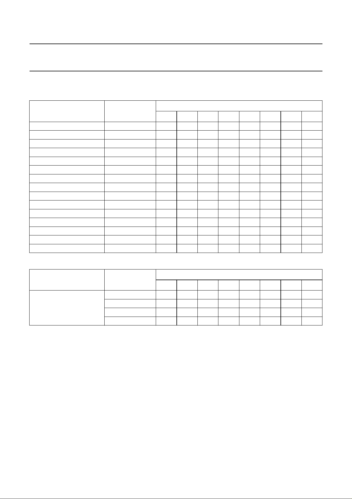
QUICK REFERENCE DATA
SYMBOL PARAMETER MIN. TYP. MAX. UNIT
Supply
V
P
I
P
supply voltage 7.2 8.0 8.8 V
supply current − 120 − mA
Input voltages
V
iVIFrms)
V
iSIF(rms)
V
iCVBS(p-p)
V
iCHROMA(p-p)
video IF amplifier sensitivity (RMS value) − 35 −µV
sound IF amplifier sensitivity (RMS value) − 30 −µV
external CVBS/Y input (peak-to-peak value) − 1.0 − V
external chroma input voltage (burst amplitude)
− 0.3 − V
(peak-to-peak value)
V
iRGB(p-p)
RGB inputs (peak-to-peak value) − 0.7 − V
Output signals
V
oCVBS(p-p)
I
oTUNER
V
oINT.(rms)
V
oAM(rms)
V
oVIDSW(p-p)
V
oB-Y(p-p)
V
oR-Y(p-p)
V
oY(BL-WH)
V
oHorizontal
V
oVertical
V
oSubc.(p-p)
demodulated CVBS output (peak-to-peak value) − 2.5 − V
tuner AGC output current range 0 − 5mA
sound IF intercarrier output (RMS value) − 100 − mV
demodulated AM sound output (RMS value) − 500 − mV
CVBS output voltage (peak-to-peak value) − 1.0/2.0 − V
−(R−Y) output voltage (peak-to-peak value) − 1.05 − V
−(B−Y) output voltage (peak-to-peak value) − 1.33 − V
Y output voltage (black-to-white value) − 1.0 − V
HA output voltage − 5 − V
VA output voltage − 5 − V
Subcarrier output amplitude (peak-to-peak value) − 200 − mV
June 30, 1998 3
Philips Semiconductors Final Device Specification
I2C-bus controlled TV Input Processor
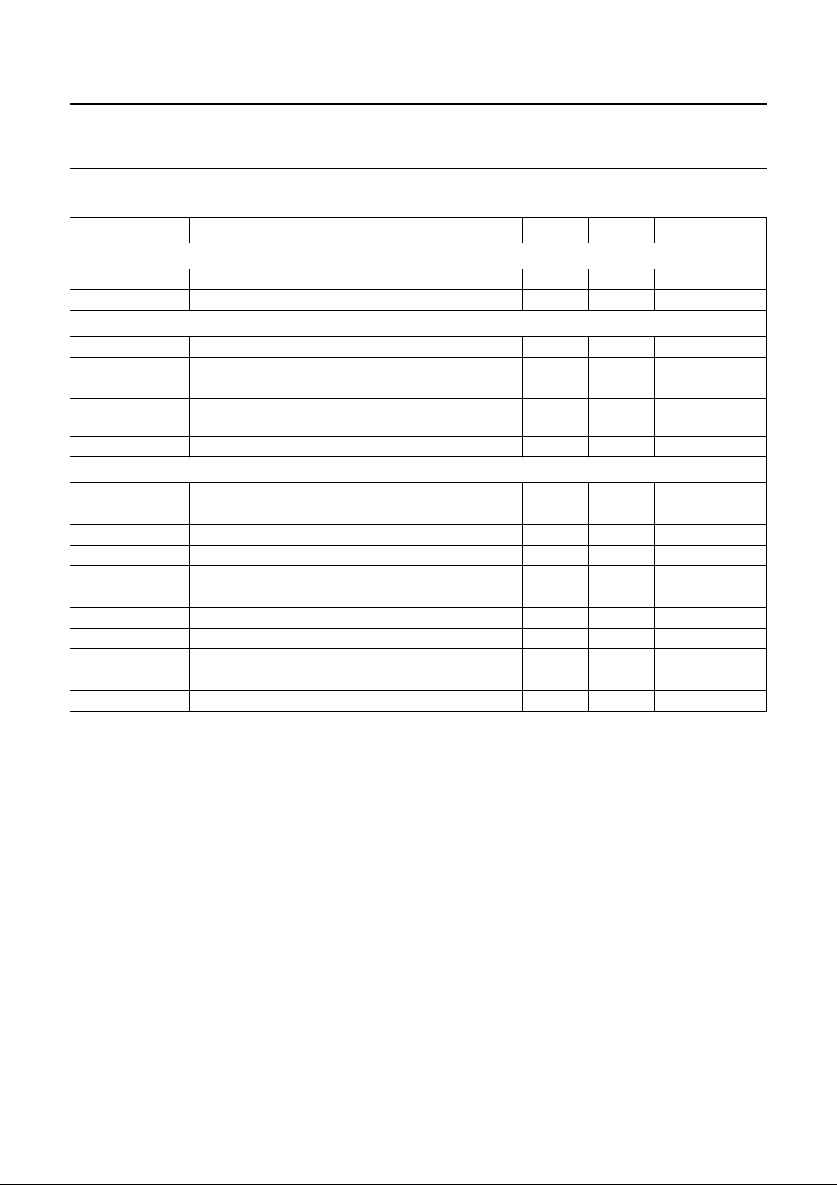
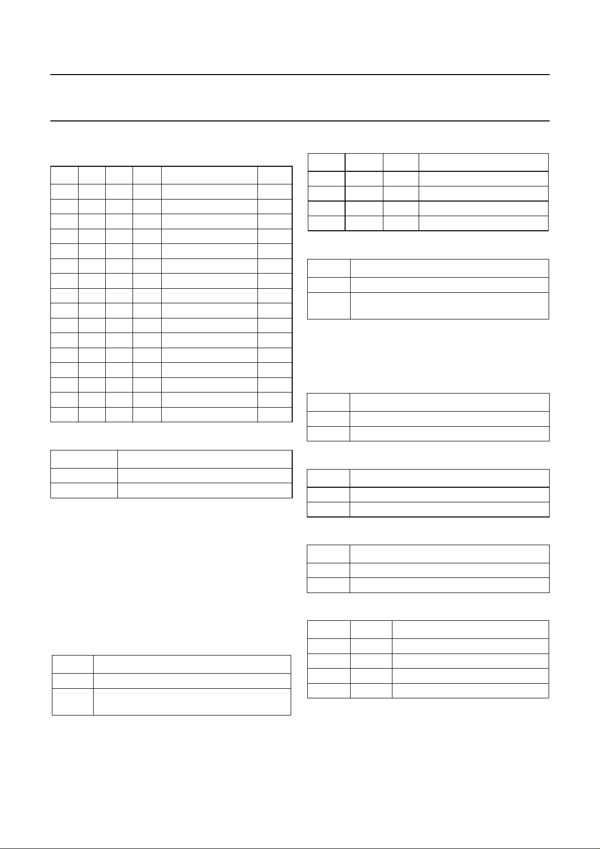
BLOCK DIAGRAM
V
Y
U
V
YU
Y/U/V
Y
Y-DELAY
VERTICAL
SWITCH
Y-DELAY
SYNC
SEPARATOR
UV
BASE-BAND
Y
Y-SWITCH
DELAY LINE
+ TRAPS
VIDEO IDENT
VA
R1 G1 B1 BL1
SDA
SCL
R2G2B2
RGB-MATRIX
C-BUS
2
I
VERTICAL
BL2
TRANSCEIVER
DIVIDER
R-Y B-Y
HELPER
/SECAM
SWITCH
PAL(NTSC)
SECAM
DECODER
SC
F
FILTER
TUNING
HUE
DEMOD.
PAL/NTSC
IDENT
SYSTEM
PLL
PAL/NTSC
HUE CONTR.
TDA 9321H
11-12-96/AC
8V
SIF-IN
VIF-IN
HA/CLP
QSS/AM
PULSE
GENERATOR
SUPPLY
AGC
SIF AMPLIFIER
TOP
AGC/AFC
PLL DEMOD
VIF AMPLIFIER
AFC
SW-OUT
TUNER
VCO+H-PLL
IDENT
QSS MIXER
AM DEMOD.
MUTE
MUTE
VIDEO AMPL.
TRAP
SOUND
SYNC
SEPARATOR
VIDEO IDENT
SWITCH
CORRECTION
GROUP DELAY
Y/CVBS
CONTROL
CVBS INT
FILTER
CLOCHE
ACC
AV-1
CVBS-1
FILTER
BANDPASS
AUTO-
CHROMA
VIDEO SWITCH + CONTROL
AV-2
CVBS-2
SW-OUT
Y(CVBS)-3
C-3
AS
C-4
Y(CVBS)-4
C
Y
SYS2
SYS1
CVBS
SUBCARRIER
Fig.1 BLOCK DIAGRAM TDA 9321H
COMB FILTER
CVBS(PIP)
CVBS(TXT)
June 30, 1998 4

Philips Semiconductors Final Device Specification
I2C-bus controlled TV Input Processor
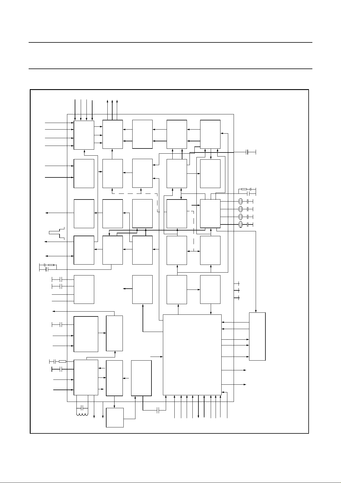
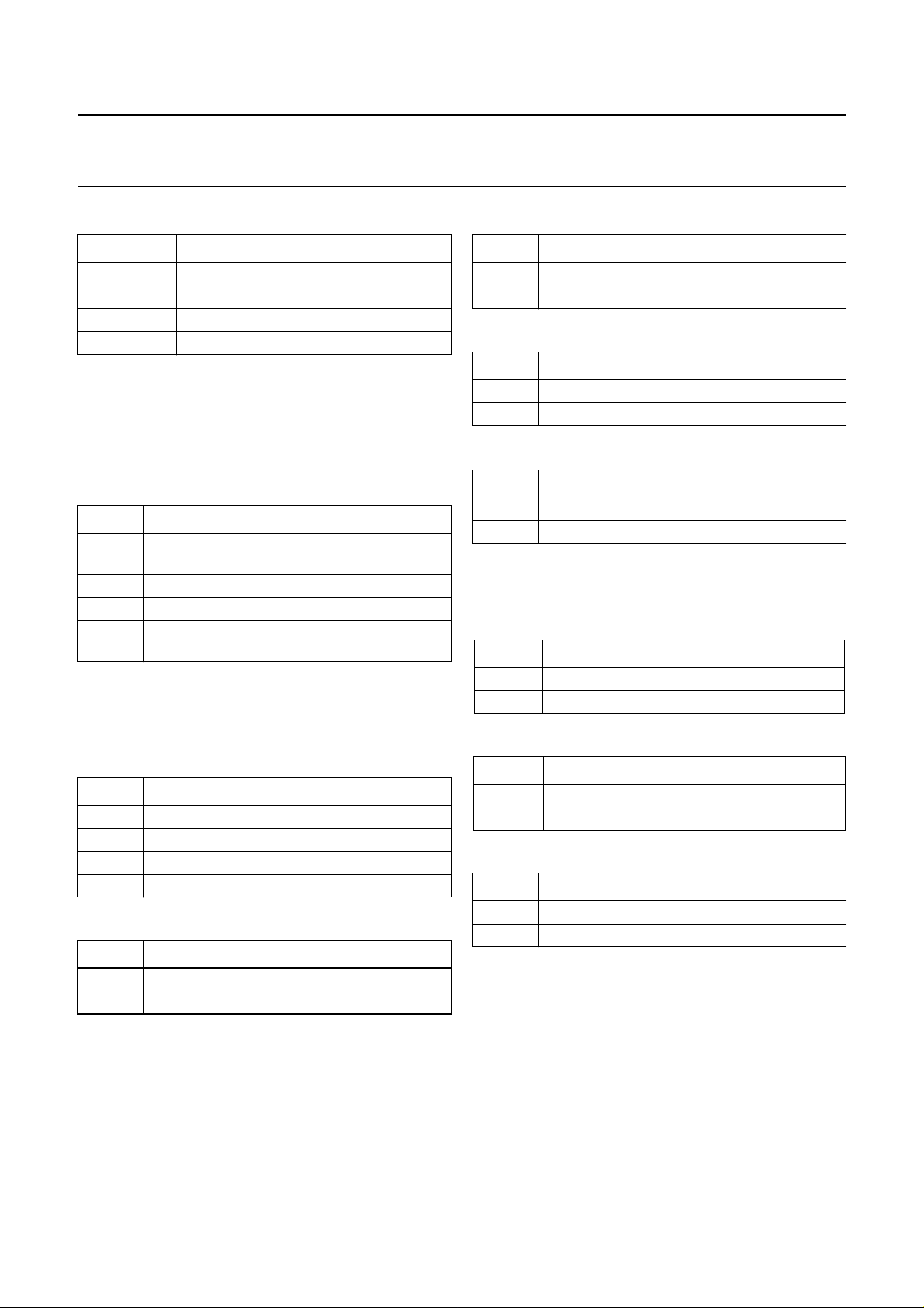
PINNING
SYMBOL PIN DESCRIPTION
AGC
SIF
IFIN1 2 IF input 1
IFIN2 3 IF input 2
AGC
VIF
SIF
/AM
OUT
OUT
PLLIF 6 IF-PLL loop filter
IFVCO1 7 IF VCO tuned circuit 1
IFVCO2 8 IF VCO tuned circuit 2
GND1 9 main ground
IFVO 10 IF video output
V
P1
GDIN 12 group delay correction input
GDOUT 13 group delay correction output
CVBS
INT
AV1 15 AV-1 input
CVBS1 16 CVBS-1 input
AV2 17 AV-2 input
CVBS2 18 CVBS-2 input
SW0 19 output switch (I2C)
CVBS/Y3 20 CVBS/Y-3 input
CHROMA3 21 chrominance-3 input
SW1 22 output switch (I2C)
CVBS/Y4 23 CVBS/Y-4 input
CHROMA4 24 chrominance-4 input
COMBSYS1 25 SYS-1 output for comb filter
COMBCVBS 26 CVBS output for comb filter
COMBSYS2 27 SYS-2 output for comb filter
COMBY 28 luminance input (from comb filter)
COMBC 29 chrominance input (from comb filter)
REFO 30 subcarrier output
GND2 31 digital ground
CVBSO
DEC
CVBSO
DEC
PIP
DIG
TXT
BG
RI1 36 R-1 input
GI1 37 G-1 input
BI1 38 B-1 input
RGBIN1 39 RGB-1 insertion input
RGBIN2 40 RGB-2 insertion input
1 SIF AGC decoupling capacitor
4 VIF AGC decoupling capacitor
5 combined QSS and AM sound output
11 main supply voltage 1 (+8 V)
14 internal CVBS input
32 CVBS (PIP) output
33 digital supply decoupling
34 CVBS (TXT) output
35 bandgap decoupling
TDA 9321H
June 30, 1998 5

Philips Semiconductors Final Device Specification
I2C-bus controlled TV Input Processor
SYMBOL PIN DESCRIPTION
RI2 41 R-2 input
GI2 42 G-2 input
BI2 43 B-2 input
GND3 44 ground
V
P2
SCL 46 serial clock input
SDA 47 serial data input/output
AS 48 address select
YO 49 luminance output
UO 50 U-output
VO 51 V-output
DET 52 loop filter burst phase detector
SECPLL 53 SECAM PLL decoupling
XTALA 54 X-tal A (4.433619 MHz)
XTALB 55 X-tal B (3.582056 MHz, PAL-N)
XTALC 56 X-tal C (3.575611 MHz, PAL-M)
XTALD 57 X-tal D (3.579545 MHz, NTSC-M)
PH1LF 58 phase-1 filter
SO 59 sandcastle pulse output
HACLP 60 HA/CLP output/input
VA 61 VA output
AGCOUT 62 tuner AGC output
SIFIN1 63 SIF input 1
SIFIN2 64 SIF input 2
45 positive supply
TDA 9321H
June 30, 1998 6
Philips Semiconductors Final Device Specification
I2C-bus controlled TV Input Processor
VA
handbook, full pagewidth
AGCSIF
IFIN1
IFIN2
AGCVIF
SIFO/AMO
PLLIF
IFVCO1
IFVCO2
GND1
IFVO
V
GDIN
GDOUT
CVBS
AV1
CVBS1
AV2
CVBS2
SW0
P1
INT
SIFIN2
64
1
2
3
4
5
6
7
8
9
10
11
12
13
14
15
16
17
18
19
SIFIN1
63
AGCOUT
62
61
HACLP
60
SO
PH1LF
59
58
TDA 9321H
XXX
XTALD
XTALC
57
56
XTALA
XTALB
55
54
SECPLL
DET
53
52
TDA 9321H
VO
51
UO
50
YO
49
48
AS
SDA
47
SCL
46
45
V
P2
44
GND3
43
BI2
GI2
42
41
RI2
RGBIN2
40
RGBIN1
39
BI1
38
37
GI1
RI1
36
DEC
35
34
33
BG
CVBSO
DEC
DIG
TXT
20
21
22
23
24
SW1
CVBS/Y3
CHROMA3
CVBS/Y4
CHROMA4
Fig.2 Pin configuration.
June 30, 1998 7
25
26
27
COMBSYS1
COMBSYS2
COMBCVBS
28
29
COMBY
COMBC
30
REFO
31
GND2
32
MXXxxx
PIP
CVBSO

Philips Semiconductors Final Device Specification
I2C-bus controlled TV Input Processor
FUNCTIONAL DESCRIPTION
Vision IF amplifier
The IF-amplifier contains 3 AC-coupled control stages with
a total gain control range which is higher than 66 dB. The
sensitivity of the circuit is comparable with that of modern
IF-IC’s.
The video signal is demodulated by means of a PLL carrier
regenerator. This circuit contains a frequency detector and
a phase detector. During acquisition the frequency
detector will tune the VCO to the right frequency. The initial
adjustment of the oscillator is realised via the I2C-bus. The
switching between SECAM L and L’ can also be realised
via the I2C-bus. After lock-in the phase detector controls
the VCO so that a stable phase relation between the VCO
and the input signal is achieved. The VCO is running at the
double IF frequency. The reference signal for the
demodulator is obtained by means of a frequency divider
circuit. To get a good performance for phase modulated
carrier signals the control speed of the PLL can be
increased by means of the FFI bit.
The AFC output is obtained by using the VCO control
voltage of the PLL and can be read via the I2C-bus. For
fast search tuning systems the window of the AFC can be
increased with a factor 3. The setting is realised with the
AFW bit.
The AGC-detector operates on top sync and top whitelevel. The demodulation polarity is switched via the
I2C-bus. The AGC detector time-constant capacitor is
connected externally. This mainly because of the flexibility
of the application. The time-constant of the AGC system
during positive modulation is rather long to avoid visible
variations of the signal amplitude. To improve the speed of
the AGC system a circuit has been included which detects
whether the AGC detector is activated every frame period.
When during 3 field periods no action is detected the
speed of the system is increased. For signals without peak
white information the system switches automatically to a
gated black level AGC. Because a black level clamp pulse
is required for this way of operation the circuit will only
switch to black level AGC in the internal mode.
The circuit contains a video identification circuit which is
independent of the synchronisation circuit. Therefore
search tuning is possible when the display section of the
receiver is used as a monitor. However, this ident circuit
cannot be made as sensitive as the slower sync ident
circuit (SL) and we recommend to use both ident outputs
to obtain a reliable search system. The ident output is
supplied to the tuning system via the I2C-bus.
TDA 9321H
The input of the identification circuit is connected to pin 14,
the “internal” CVBS input (see Fig.3). This has the
advantage that the ident circuit can also be made
operative when a scrambled signal is received
(descrambler connected between the IF video output (pin
10) and pin 14). A second advantage is that the ident
circuit can be used when the IF amplifier is not used (e.g.
with built-in satellite tuners).
The video ident circuit can also be used to identify the
selected CBVS or Y/C signal. The switching between the
2 modes can be realised with the VIM bit.
The TDA 9321H contains a group delay correction circuit
which can be switched between the BG and a flat group
delay response characteristic. This has the advantage that
in multi-standard receivers no compromise has to be made
for the choice of the SAW filter. Both the input and output
of the group delay correction circuit are externally available
so that the sound trap can be connected between the IF
video output and the group delay correction input. The
output signal of the correction circuit can be supplied to the
video processing circuit and to the SCART plug.
2
The IC has several (I
can be used to switch sound traps or other external
components.
When the IF amplifier is not used the complete IF amplifier
can be switched-off via the I2C-bus by means of the IFO
bit.
Sound circuit
The sound IF amplifier is similar to the vision IF amplifier
and has a gain control range of about 66 dB. The AGC
circuit is related to the SIF carrier levels (average level of
AM or FM carriers) and ensures a constant signal
amplitude of the AM demodulator and the QSS mixer.
The single reference QSS mixer is realised by a multiplier.
In this multiplier the SIF signal is converted to the
intercarrier frequency by mixing it with the regenerated
picture carrier from the VCO. The mixer output signal is
supplied to the output via a high-pass filter for attenuation
of the residual video signals. With this system a high
performance hi-fi stereo sound processing can be
achieved.
The AM sound demodulator is realised by a multiplier. The
modulated sound IF signal is multiplied in phase with the
limited SIF signal. The demodulator output signal is
supplied to the output via a low-pass filter for attenuation
of the carrier harmonics.
C-bus controlled) output ports which
June 30, 1998 8
Philips Semiconductors Final Device Specification
I2C-bus controlled TV Input Processor
VIM
IDENT
CVBS
EXT. 2
Y/CVBS
EXT. 3
EXT. 3
Fig.3 CVBS switch and interfacing of video ident
CVBS-INT
VIDEO
IDENT
CVBS
EXT. 1
TDA 9321H
TO LUMA/SYNC PROCESSING
TO CHROMA PROCESSING
+
+
+
C
Y/CVBS
EXT. 4CEXT. 4
COMB C-IN
COMB Y-IN
CVBS
COMB OUT
TXT
CVBSO
PIP
CVBSO
Video switches
The circuit has 3 CVBS inputs (1 internal and 2 external
inputs) and 2 Y/C inputs. The Y/C inputs can also be used as
additional CVBS inputs. The switch configuration is given in
Fig.3. The selection of the various sources is made via the
I2C-bus.
The circuit can be set in a mode in which it automatically
detects whether a CVBS or a Y/C signal is supplied to the Y/C
inputs. In this mode the TV-standard identification first takes
place on the added Y/CVBS and the C input signal. Then both
chroma input signal amplitudes are checked once and the
input signal with the highest burst signal amplitude is
selected. The result of the detection can be read via the
I2C-bus.
The IC has 2 inputs (AV-1 and AV-2) which can be used to
read the status levels of pin 8 of the SCART plug. The
information is available in the output status byte 02 in the bits
D0-D3.
The 3 outputs of the video switch (CVBSO
, CVBSO
TXT
PIP
and
COMBCVBS) can be independently switched to the various
input signals. The names are just arbitrary and it is for
instance possible to use the COMBCVBS signal to drive the
Comb-filter and the teletext decoder in parallel and to supply
the CVBSO
signal to the SCART plug (via an emitter
TXT
follower).
For comb filter interfacing the circuit has the
COMBCVBS output, a 3rd Y/C input, a reference signal
output (fsc) and 2 control pins which switch the comb
filter to the standard of the incoming signal (as detected
by the ident circuit of the colour decoder). When a signal
is recognised which can be combed and the comb filter
is enabled by the ECMB-bit the Y/C signals coming from
the comb filter are automatically selected. This is
indicated via the CMB-bit in output status byte 02
(D5).For signals which cannot be combed (like SECAM
or Black-to-White signals) the Y/C signals coming from
the comb filter are not selected.
Chroma and luminance processing
The circuits contain a chroma bandpass, the SECAM
cloche filter and chroma trap circuit. The filters are
realised by means of gyrator circuits and they are
automatically calibrated by comparing the tuning
frequency with the X-tal frequency of the decoder. The
luminance delay line is also realised by means of gyrator
circuits. The centre frequency of the chroma bandpass
filter is switchable via the I2C-bus so that the
performance can be optimised for “front-end” signals
and external CVBS signals.
The luminance output signal which is derived from the
incoming CVBS or Y/C signal can be varied in amplitude
by means of a separate gain setting control via the
I2C-bus control bits GAI1 and GAI0. The gain variation
which can be realised with these bits is -1 to +2 dB.
June 30, 1998 9

Philips Semiconductors Final Device Specification
I2C-bus controlled TV Input Processor
Colour decoder
The colour decoder can decode PAL, NTSC and SECAM
signals. The PAL/NTSC decoder contains an
alignment-free X-tal oscillator with 4 separate X-tal pins, a
killer circuit and two colour difference demodulators. The
90° phase shift for the reference signal is made internally.
Because it is possible to connect 4 different X-tals to the
colour decoder, all colour standards can be decoded
without external switching circuits. Which X-tals are
connected to the decoder must be indicated via the
I2C-bus. X-tal pins which are not used must be left open.
The horizontal oscillator is calibrated by means of the X-tal
frequency of the colour PLL. For a reliable calibration it is
very important that the X-tal indication bits (XA to XD) are
not corrupted. For this reason the X-tal bits can be read in
the output bytes so that the software can check the I2C
transmission.
The IC’s contain an Automatic Colour Limiting (ACL)
circuit which is switchable via the I2C-bus and which
prevents that oversaturation occurs when signals with a
high chroma-to-burst ratio are received. The ACL circuit is
designed such that it only reduces the chroma signal and
not the burst signal. This has the advantage that the colour
sensitivity is not affected by this function. The ACL function
is mainly intended for NTSC signals and it can also be
used for PAL signals. For SECAM signals the ACL function
should be switched-off.
The SECAM decoder contains an auto-calibrating PLL
demodulator which has two references, viz: the 4.43 MHz
sub-carrier frequency which is obtained from the X-tal
oscillator which is used to tune the PLL to the desired
free-running frequency and the bandgap reference to
obtain the correct absolute value of the output signal. The
VCO of the PLL is calibrated during each vertical blanking
period, when the IC is in search or SECAM mode.
The circuit can also decode the PAL
can insert the various reference signals, set-ups and
timing signals which are required for the PAL
IC’s.
The base-band delay line (TDA 4665 function) is
integrated.
plus
helper signal and
plus
decoder
TDA 9321H
RGB switch and matrix
The IC has 2 RGB inputs with fast switching. The switching
of the various sourcing is controlled via the I2C-bus and the
condition of the switch inputs can be read from the I2C-bus
status bytes. If the RGB signals are not synchronous with
the selected decoder input signal, an external clamp pulse
has to be supplied to the HA/CLP input. The IC must be set
in this mode via the I2C-bus. In that case the VA pulse is
suppressed by switching the VA output in a high
impedance OFF-state.
When an external RGB signal is mixed into the internal
YUV signal it is necessary to switch-off the PAL
demodulation. To detect the presence of a fast blanking a
circuit is added which forces the MACP and HD bit to zero
if a blanking pulse is detected in 2 consecutive lines. This
system is chosen to prevent switching-off at every spike
which is detected on the fast blanking input.
The IC has the possibility to use the RGB1 input as YUV
input. This function can be enabled by means of the YUV
bit in subaddress 0A (D3). When switched to the YUV input
the input signals must have the same amplitude and
polarity as the YUV output signals. The Y signal has to be
supplied to the G1 input, the U signal to the B1 input and
the V signal to the R1 input.
Synchronisation circuit
The sync separator is preceded by a controlled amplifier
which adjusts the sync pulse amplitude to a fixed level.
These pulses are fed to the slicing stage which is operating
at 50% of the amplitude. The separated sync pulses are
fed to the phase detector and to the coincidence detector.
This coincidence detector is used to detect whether the
line oscillator is synchronised and can also be used for
transmitter identification. This circuit can be made less
sensitive by means of the STM bit. This mode can be used
during search tuning to avoid that the tuning system stops
at very weak input signals. The PLL has a very high statical
steepness so that the phase of the picture is independent
of the line frequency.
For the horizontal output pulse 2 conditions are possible,
viz.:
• An HA pulse which has a phase and width which is
identical to the incoming horizontal sync pulse
• A clamp pulse (CLP) which has a phase and width which
is identical to the clamp pulse in the sandcastle pulse
plus
June 30, 1998 10

Philips Semiconductors Final Device Specification
I2C-bus controlled TV Input Processor
The HA/CLP signal is generated by means of an oscillator
which is running at a frequency of 440 x fH. Its frequency is
divided by 440 to lock the first loop to the incoming signal.
The time-constant of the loop can be forced by the I2C-bus
(fast or slow). If required the IC can select the
time-constant depending on the noise content of the
incoming video signal.
The free-running frequency of the oscillator is determined
by a digital control circuit which is locked to the reference
signal of the colour decoder. When the IC is switched-on
the HA/CLP is suppressed and the oscillator is calibrated
as soon as all sub-address bytes have been sent. When
the frequency of the oscillator is correct the HA/CLP signal
is switched-on again.
When the coincidence detector indicates an out-of-lock
situation the calibration procedure is repeated.
The VA pulse is obtained via a vertical count down circuit.
The countdown circuit has various windows depending on
the incoming signal (50 Hz or 60 Hz standard or no
standard). The countdown circuit can be forced in various
modes by means of the I2C-bus. To obtain short switching
times of the countdown circuit during a channel change the
divider can be forced in the search window by means of
the NCIN bit.
TDA 9321H
2
C-BUS SPECIFICATION
I
The slave addresses of the IC’s is given in the table below.
The circuit operates up to clock frequencies of 400 kHz.
Slave addresses
A6 A5 A4 A3 A2 A1 A0 R/W
1 0 0 0 1 A1 1 1/0
The bit A1 is controlled via the pin 48 (AS), when the pin is
connected to ground it is a 0 and when connected to the
positive supply line it is a 1. When this pin is left open it is
connected to ground via an internal resistor.
Start-up procedure
Read the status bytes until POR = 0 and send all
subaddress bytes. It is advised to check the bus
transmission by reading the output status bits SXA to SXD.
This ensures a good operation of the calibration system of
the horizontal oscillator. The horizontal output signal is
switched-on when the oscillator is calibrated.
Each time before the data in the IC is refreshed, the status
bytes must be read. If POR = 1, the procedure mentioned
above must be carried out to restart the IC.When this
procedure is not followed the horizontal frequency may be
incorrect after power-up or after a power dip.
Valid subaddresses: 00 to 0E, subaddresses FE and FF
are reserved for test purposes. Auto-increment mode
available for subaddresses.
June 30, 1998 11
Philips Semiconductors Final Device Specification
I2C-bus controlled TV Input Processor
Inputs
Table 1 Input status bits.
FUNCTION
Colour decoder 0 00 CM3 CM2 CM1 CM0 XD XC XB XA
Colour decoder 1 01 MACP HOB HBC HD 0 ACL CB BPS
Luminance 02 0 0 GAI1 GAI0 YD3 YD2 YD1 YD0
Hue control 03 0 0 A5 A4 A3 A2 A1 A0
Spare 04 0 0 000000
Synchronisation 0 05 FORF FORS FOA FOB 0 VIM POC VID
Synchronisation 1 06 0 0 0 0 BSY HO EMG NCIN
Spare 07 0 0 000000
Video switches 0 08 0 0 0 ECMB DEC3 DEC2 DEC1 DEC0
Video switches 1 09 0 PIP2 PIP1 PIP0 0 TXT2 TXT1 TXT0
RGB switch 0A 0 0 0 0 YUV ECL IE2 IE1
Output switches 0B 0 0 0000OS1OS0
Vision IF 0C FFI IFO GD MOD AFW IFS STM VSW
Tuner take-over 0D 0 0 A5 A4 A3 A2 A1 A0
Adjustment IF PLL 0E L’FA A6 A5 A4 A3 A2 A1 A0
SUBADDRESS
(HEX)
D7 D6 D5 D4 D3 D2 D1 D0
DATA BYTE
TDA 9321H
Table 2 Output status bits.
FUNCTION
Output status bytes 00 POR x x x SNR FSI SL IVW
SUBADDRESS
(HEX)
01 CD3 CD2 CD1 CD0 SXD SXC SXB SXA
02 IN1 IN2 CMB YC S2A S2B S1A S1B
03 ID3 ID2 ID1 ID0 IFI PL AFA AFB
D7 D6 D5 D4 D3 D2 D1 D0
DATA BYTE
June 30, 1998 12
Philips Semiconductors Final Device Specification
I2C-bus controlled TV Input Processor
INPUT CONTROL BITS
Table 3 Colour decoder mode
CM3 CM2 CM1 CM0 DECODER MODE X-TAL
0 0 0 0 PAL/NTSC/SECAM A
0 0 0 1 PAL/NTSC A
0010PAL A
0 0 1 1 NTSC A
0 1 0 0 SECAM A
0 1 0 1 PAL/NTSC B
0110PAL B
0 1 1 1 NTSC B
1 0 0 0 PAL/NTSC/SECAM ABCD
1 0 0 1 PAL/NTSC C
1010PAL C
1 0 1 1 NTSC C
1 1 0 0 spare
1 1 0 1 PAL/NTSC D
1110PAL D
1 1 1 1 NTSC D
Table 4 X-tal indication
TDA 9321H
Table 6 Helper output blanking (PAL
HOB HBC SNR BLANKING
0--off
10-on
110off
111on
plus
Table 7 PAL
helper demodulation active, note1
HD CONDITION
0off
1 on, PAL
plus
mode with helper set-up 400 mV
and black set-up 200 mV
Note
1. Black and helper set-up will only be present in a norm
sync condition.
Table 8 Automatic colour limiting
ACL COLOUR LIMITING
0 not active
1 active
plus
/EDTV-2)
XA-XD CONDITION
0 X-tal not present
1 X-tal present, note1
Note
1. When a comb filter is used the various X-tals must be
connected to the IC as indicated in the pinning
diagram. This is required because the ident system
switches automatically to the comb filter when a signal
is identified which can be combed (right combination of
colour standard and X-tal frequency). For applications
without comb filter only XA is important (4.43 MHz),
the other pins can then have an arbitrary 3.5 MHz
X-tal.
Table 5 Motion Adaptive Colour Plus, note1
MACP MODE
0 internal 4.43 MHz trap used
1 external MACP chroma filtering used, 4.43
MHz trap bypassed, black set-up 200 mV
Note
1. The black set-up will only be present in a norm sync
condition.
Table 9 Chroma bandpass centre frequency
CB CENTRE FREQUENCY
0F
1 1.1 x F
SC
SC
Table 10 Bypass of chroma base-band delay line
BPS DELAY LINE MODE
0 active
1 bypassed
Table 11 Gain luminance channel
GAI1 GAI0 GAIN SETTING
0 0 -1 dB
0 1 0 dB
1 0 +1 dB
1 1 +2 dB
June 30, 1998 13
Philips Semiconductors Final Device Specification
I2C-bus controlled TV Input Processor
Table 12 Y-delay adjustment; note 1
YD0 to YD3 Y-DELAY
YD3 YD3 ∗ 160 ns +
YD2 YD2 ∗ 160 ns +
YD1 YD1 ∗ 80 ns +
YD0 YD0 ∗ 40 ns
Note
1. For an equal delay of the luminance and chrominance
signal the delay must be set at a value of 280 ns
(YD3...YD0 = 1011). This is only valid for a CVBS
signal without group delay distortions.
Table 13 Forced field frequency
FORF FORS FIELD FREQUENCY
0 0 auto (60 Hz when line not
synchronized)
0 1 forced 60 Hz; note 1
1 0 keep last detected field frequency
1 1 auto (50 Hz when line not
synchronized)
Note
1. When switched to this mode the divider will directly
switch to forced 60 Hz only.
Table 14 Phase 1 (ϕ1) time constant, see also table 55
FOA FOB MODE
0 0 normal
0 1 slow
1 0 slow/fast
1 1 fast
Table 15 Video ident mode
VIM MODE
0 ident coupled to internal CVBS (pin 14)
1 ident coupled to selected CVBS
TDA 9321H
Table 16 Synchronization mode
POC MODE
0 active
1 not active
Table 17 Video ident mode
VID VIDEO IDENT MODE
0 ϕ
1 not active
Table 18 Blanked sync on Y
BSY CONDITION
0 unblanked sync, note1
1 blanked sync
Note
1. Except for PAL
Table 19 Condition of horizontal output
HO CONDITION
0 clamp pulse available at H
1HA pulse available at H
Table 20 Enable “Macrovision/subtitle” gating
EMG MODE
0 disable gating
1 enable gating
Table 21 Vertical divider mode
NCIN VERTICAL DIVIDER MODE
0 normal operation
1 switched to search window
loop switched on and off
1
out
plus
with black set-up.
OUT
OUT
June 30, 1998 14
 Loading...