


DATA SH EET
Preliminary specification
File under Integrated Circuits, IC02
1999 Sep 24
INTEGRATED CIRCUITS
TDA9178
YUV one chip picture improvement
based on luminance vector-, colour
vector- and spectral processor

1999 Sep 24 2
Philips Semiconductors Preliminary specification
YUV one chip picture improvement based on luminance
vector-, colour vector- and spectral processor
TDA9178
FEATURES
• Picture content dependent non-linear Y, U and V
processing by luminance histogram analysis
• Variable gamma control
• Adaptive black and white stretch control
• Skin tone correction
• Green enhancement
• Blue stretch
• Luminance Transient Improvement (LTI)
• Smart peaking for detail enhancement
• Colour Transient Improvement (CTI)
• SCAn VElocity Modulation (SCAVEM) output
• Line Width Control (LWC)
• Video Dependent Coring (VDC)
• Colour Dependent Sharpness (CDS)
• Noise measurement
• Feature Mode (FM) detector
• Cue Flash (CF) detector
• Three additional pins for access to 6-bit ADC and
I2C-bus
• Adjustable chrominance delay
• TV standard independent
• I2C-bus controlled
• 1fH and 2f
H
• DEmonstration MOde (DEMO).
GENERAL DESCRIPTION
The TDA9178 is a transparent analog video processor
with YUV input and output interfaces. It offers three main
functions: luminance vector processing, colour vector
processing and spectral processing. Beside these three
main functions, there are some additional functions.
In the luminancevector processor, the luminance transfer
function is controlled in a non-linear way by the
distribution, in 5 discrete histogram sections, of the
luminance values measured in a picture. As a result, the
contrast ratio of the most important parts of the scene will
be improved. Black restoration is available in the event of
a set-up in the luminance signal.
A variable gamma function, after the histogram
conversion,offersthepossibilitiesofalternativebrightness
control or factory adjustment of the picture tube.
The adaptive black stretch function of the TDA9178 offers
the possibility of having a larger ‘weight’ for the black parts
of the video signal; the white stretch function offers an
additional overall gain for increased light production.
To maintain a proper colour reproduction, the saturation of
theU- and V-colour difference signals is also controlledas
a function of the actual non-linearity in the luminance
channel.
In the colour vector processor, the dynamic skin tone
correction locally changes the hue of colours that match
skin tones to the correct hue. The green enhancement
circuit activates medium saturated green towards to more
saturated green. The blue stretch circuit can be activated
which shifts colours near white towards blue.
The spectral processor provides 1D luminance transient
improvement, luminance detail enhancement by smart
peaking and a 1 D colour transient improvement.
The TDA9178 can be used as a cost effective alternative
to (but also in combination with) scan velocity modulation.
In the spectral processor line width control (or aperture
control) can be user defined. The TDA9178 is capable of
adjusting the amount of coring according to the video level
with the video dependent coring. The TDA9178 is also
capable to give extra sharpness in the cases of saturated
red and magenta parts of the screen using the colour
dependent sharpness feature.
An embedded noise detector measures noise during the
field retrace in parts which are expected to be free from
video or text information. With the noise detector a variety
of ‘smart noise control’ architectures can be set up.
A feature mode detector is available for detecting signal
sources like VCR (in still picture mode) that re-insert the
levels of the retrace part. For this kind of signals the noise
measurement of the TDA9178 is not reliable.
An output signal (on the I2C-bus and on a separate pin) is
available that detects when the picture content has been
changed significantly, called cue flash.
An embedded 6-bit ADC can be used for interfacing three
analog low frequency voltage signals (e.g. ambient light
control or beam current voltage level) to the I2C-bus.

1999 Sep 24 3
Philips Semiconductors Preliminary specification
YUV one chip picture improvement based on luminance
vector-, colour vector- and spectral processor
TDA9178
In the demonstration mode all the features selected by the user are automatically toggled between on and off.
The TDA9178 concept has a maximum flexibility which can be controlled by the embedded I2C-bus. The supply voltage
is 8 V. The device is mounted in a 24-lead SDIP package, or in a 24-lead SO package.
QUICK REFERENCE DATA
ORDERING INFORMATION
SYMBOL PARAMETER CONDITIONS MIN. TYP. MAX. UNIT
V
CC
supply voltage 7.2 8.0 8.8 V
V
i(Y)
luminance input voltage (excluding sync) AMS = 0 − 0.315 0.45 V
AMS = 1 − 1.0 1.41 V
V
i(UV)
UV input voltage −−1.9 V
V
FS(ADC)
full-scale ADC input voltage − 2.0 − V
TYPE
NUMBER
PACKAGE
NAME DESCRIPTION VERSION
TDA9178 SDIP24 plastic shrink dual in-line package; 24 leads (400 mil) SOT234-1
TDA9178T SO24 plastic small outline package; 24 leads; body width 7.5 mm SOT137-1
1999 Sep 24 4
Philips Semiconductors Preliminary specification
YUV one chip picture improvement based on luminance
vector-, colour vector- and spectral processor
TDA9178
This text is here in white to force landscape pages to be rotated correctly when browsing through the pdf in the Acrobat reader.This text is here in
_white to force landscape pages to be rotated correctly when browsing through the pdf in the Acrobat reader.This text is here inThis text is here in
white to forcelandscapepages to be rotated correctly when browsing through the pdf in the Acrobat reader. white to force landscape pages to be ...
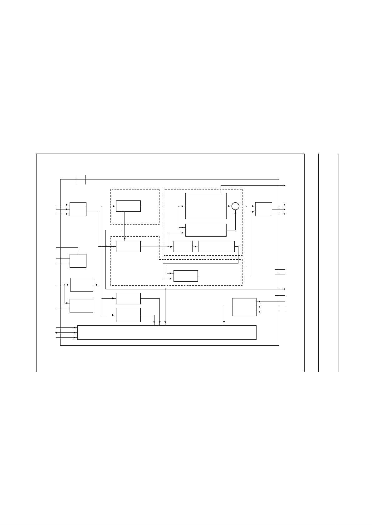
BLOCK DIAGRAM
handbook, full pagewidth
MGR897
VIDEO DEPENDENT
CORING
LUMINANCE TRANSIENT
IMPROVEMENT
SMART PEAKING
COLOUR DEPENDENT
SHARPNESS
COLOUR
PROCESSING
SATURATION
CORRECTION
LUMINANCE
PROCESSING
OUTPUT
STAGE
COLOUR TRANSIENT
IMPROVEMENT
DELAY
CONTROL
YOUT
UOUT
VOUT
19
SOUT
21
CF
22
17
16
NOISE
MEASURING
FEATURE
MODE
DETECTION
INPUT
STA GE
YIN
UIN
VIN
6
n.c.12n.c.
13
8
9
WINDOW
GENERATION
SC
1
SUPPL Y
V
CC
V
EE
20
15
18
SDA
14
ADR
7
SCL
11
ANALOG
TO
DIGITAL
CONVERTER
ADEXT1
ADEXT2
ADEXT3
3
n.c.
2
n.c.
23
n.c.
24
4
5
spectral processingluminance vector processing
colour vector
processing
black stretch
histogram processing
gamma control
skin tone correction
green enhancement
blue stretch
Y
U, V
cue flash
I2C-BUS CONTROL
DEC
DIG
CALIBRATE
TP
10
+
Fig.1 Block diagram.
1999 Sep 24 5
Philips Semiconductors Preliminary specification
YUV one chip picture improvement based on luminance
vector-, colour vector- and spectral processor
TDA9178
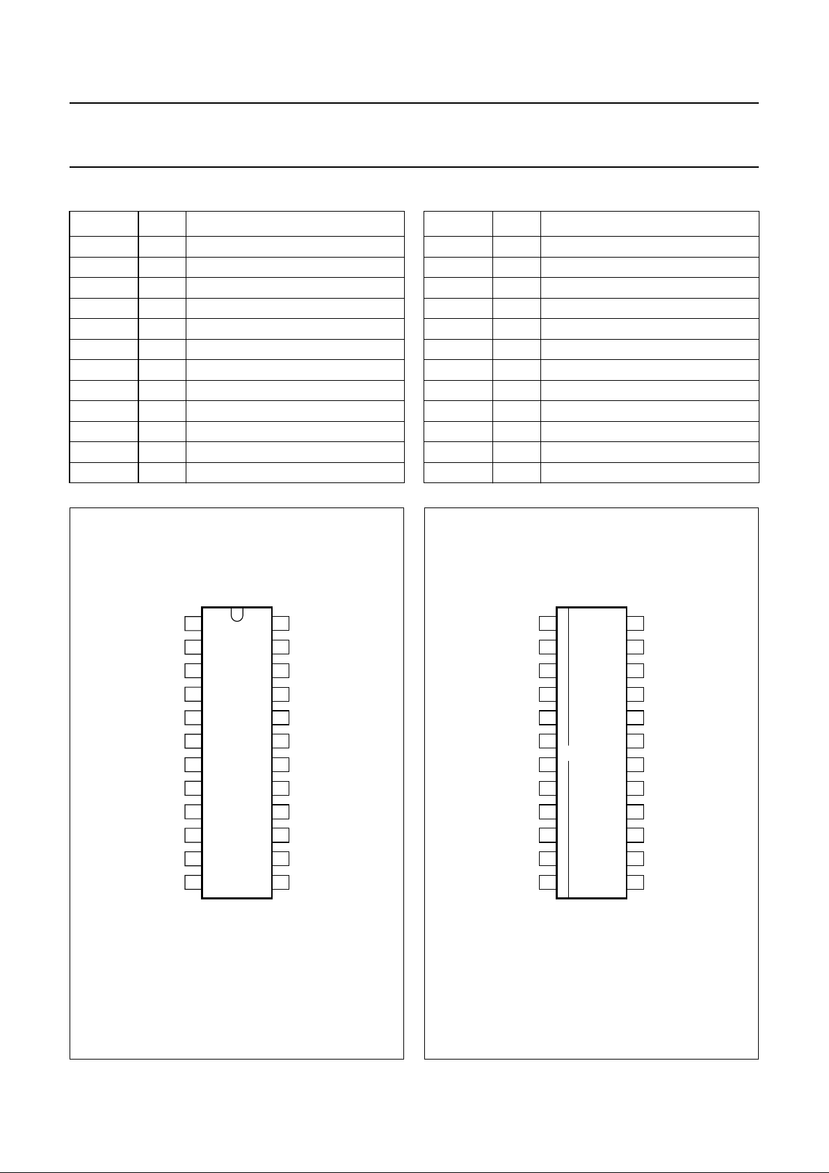
PINNING
SYMBOL PIN DESCRIPTION
SC 1 sandcastle input
n.c. 2 not connected
ADEXT1 3 ADC input 1
ADEXT2 4 ADC input 2
ADEXT3 5 ADC input 3
YIN 6 luminance input
ADR 7 address selection input
UIN 8 U signal input
VIN 9 V signal input
TP 10 test pin
SCL 11 serial clock input (I
2
C-bus)
n.c. 12 not connected
n.c. 13 not connected
SDA 14 serial data input/output (I
2
C-bus)
DEC
DIG
15 decoupling digital supply
VOUT 16 V signal output
UOUT 17 U signal output
V
EE
18 ground
YOUT 19 luminance output
V
CC
20 supply voltage
SOUT 21 SCAVEM output
CF 22 cue flash output
n.c. 23 not connected
n.c. 24 not connected
SYMBOL PIN DESCRIPTION
Fig.2 Pin configuration (SOT234-1).
handbook, halfpage
SC
n.c.
ADEXT1
ADEXT2
ADEXT3
YIN
ADR
UIN
VIN
TP
SCL
n.c.
n.c.
n.c.
CF
SOUT
YOUT
V
EE
V
CC
UOUT
VOUT
DEC
DIG
SDA
n.c.
1
2
3
4
5
6
7
8
9
10
11
12
24
23
22
21
20
19
18
17
16
15
14
13
TDA9178
MGR898
Fig.3 Pin configuration (SOT137-1).
handbook, halfpage
SC
n.c.
ADEXT1
ADEXT2
ADEXT3
YIN
ADR
UIN
VIN
TP
SCL
n.c.
n.c.
n.c.
CF
SOUT
YOUT
V
EE
V
CC
UOUT
VOUT
DEC
DIG
SDA
n.c.
1
2
3
4
5
6
7
8
9
10
11
12
24
23
22
21
20
19
18
17
16
15
14
13
TDA9178T
MGR899

1999 Sep 24 6
Philips Semiconductors Preliminary specification
YUV one chip picture improvement based on luminance
vector-, colour vector- and spectral processor
TDA9178
FUNCTIONAL DESCRIPTION
Y input selection and amplification
The gain of the luminance input amplifier and output
amplifier can be adjusted to signal amplitudes of
0.315 and 1.0 V typically (excluding sync) by I2C-bus
bit AMS. The sync part is processed transparently to the
output, independently of the feature settings.
The Y, U and V input signals are clamped during the
burstkey period, defined by the sandcastle reference and
should be DC-coupled (the circuit uses internal clamp
capacitors). During the clamp pulse (see Figs 7, 8, 9
and 10) an artificial black level is inserted in the Y input
signal to correctly preset the internal circuitry.
Luminance vector processor
Intheluminancevectorprocessorthetransfer is controlled
bya black stretch, the histogramprocessing and a gamma
control circuit. The luminance vector processor also
creates the cue flash signal.
BLACK STRETCH
Ablack detector measures and stores thelevelof the most
black part of the scene within an internal defined fixed
window in each field into a time constant. The time
constant and the response time of the loop are internally
fixed. Any difference between this value and the value
measured during the clamp is regarded as black offset.
In a closed loop offsets until a predefined value of the fullscale value are fed back to the input stage for
compensation.The loop gain is afunction of the histogram
and variable gamma settings. The black offset correction
can be switched on and off by the I2C-bus bit BON.
Related to the corrected black offset the nominal signal
amplitude is set again to 100% full scale through an
amplitude stretch function. Luminance values beyond full
scale are unaffected. Additionally, the measured black
offset is also used to set the adaptive black stretch gain
(see also Section “Adaptive black stretch”).
HISTOGRAM PROCESSING
For the luminance signal the histogram distribution is
measured in real-time over five segments within an
internally defined fixed window in each field. During the
period that the luminance is in one segment, a
corresponding internal capacitor is loaded by a current
source. At the end of the field five segment voltages are
stored into on-board memories. The voltages stored in the
memories determine the non-linear processing of the
luminance signal to achieve a picture with a maximum of
information (visible details).
Each field the capacitors are discharged and the
measurement starts all over again.
Parts in the scene that do not contribute to the information
inthatscene,likesub or side titles,should be omitted from
the histogram measurement. No measurements are
performed outside the internal fixed window period.
Very rapid picture changes, also related to the field
interlace,canresultinflickereffects.The histogram values
are averaged at the field rate thus cancelling the flicker
effects.
Adaptive black stretch
The so-called adaptive black stretch gain is one of the
factors that control the gamma of the picture. This gain is
controlled by the measured black offset value in the black
stretch circuit and theI2C-bus adaptive black stretchDAC:
bits BT5 to BT0. For pictures with no black offset the black
stretchgainequalsunitysothegammaisnotchanged and
the DAC setting has no influence. In case of a black offset,
the black stretch gain is increased so the gamma of the
pictureis reduced. This procedure results in amaximumof
visible details over the whole range of luminances.
However, depending on personal taste, sometimes higher
values of gamma are preferred. Therefore the amount of
gamma reduction can be adjusted by the DAC.
Adaptive white-point stretching
Forpictureswithmany details in white parts, the histogram
conversion procedure makes a transfer with large gain in
the white parts. The amount of light coming out of the
scene is reduced accordingly. The white stretcher
introduces additional overall gain for increased light
production, and so violating the principle of having a
full-scale reference. The white-point stretching can be
switched on or off by means of the I2C-bus bit WPO.
Standard deviation
Forscenesin which segments of the histogram distribution
areverydominant with respect to the others, the non-linear
amplification should be reduced in comparison to scenes
with a flat histogram distribution. The standard deviation
detectormeasuresthe spread of the histogram distribution
and modulates the user setting of the non-linear amplifier.
Non-linear amplifier
Thestoredsegmentvoltagesdeterminetheindividualgain
of each segment in such a way that continuity is granted
for the complete luminance range.

1999 Sep 24 7
Philips Semiconductors Preliminary specification
YUV one chip picture improvement based on luminance
vector-, colour vector- and spectral processor
TDA9178
The maximum and minimum gain of each segment is
limited. Apart from the adaptive white-point stretching the
black and white references are not affected by the
non-linear processing. The amount of non-linearity can be
controlled by the I2C-bus non-linearity DAC:
bits NL5 to NL0.
VARIABLE GAMMA
On top of the histogram conversion a variable gamma
function is applied for an alternative brightness control, or
for factory adjustment. It is intended as an alternative for
the DC-offset of the classic brightness user control.
It maintains the black and white references. The gamma
ranges from 0.5 to 1.5. The gamma can be set by the
I2C-bus variable gamma DAC: bits VG5 to VG0.
CUE FLASH
In the present TV environment there is a lot of measured
information like ambient light and noise. This information
can be used to make an update of settings of the several
algorithms after a picture has changed. The cue flash
signal detects when a picture changes significantly. When
the picture content has changed, the I2C-bus bit CF is set
to logic 1 in the status register. After reading the status
register, bit CF is reset to logic 0. On the output pin CF the
cue flash information is present (active LOW) for only one
line in the vertical retrace part. This pin is configured as an
open drain output and therefore should be pulled up to the
5 V supply.
Spectral processor
In the spectral processor the luminance transfer is
controlled by smart peaking, colour dependent sharpness
and luminance transient improvement, defined by the
sharpness improvement processor. The colour transfer is
controlled by a colour transient improvement circuit; an
additional output is available to provide a SCAVEM circuit.
ADJUSTABLE CHROMINANCE DELAY
The colour vector processor drives a delay line for
correctingdelayerrors between the luminance input signal
and the chrominance input signals (U and V).
The chrominance delay can be adjusted in 6 steps of
12 ns (1fH) or 6 ns (2fH) by the I2C-bus bits CD2 to CD0.
SHARPNESS IMPROVEMENT PROCESSOR
The sharpness improvement processor increases the
slope of large luminance transients of vertical objects and
enhancestransientsof details in natural scenes by contour
correction.
It comprises three main processing units: the step
improvement processor, the contour processor and the
smart sharpness controller.
Transient improvement processor
The step improvement processor (see Fig.11) comprises
two main functions:
• MINMAX generator
• MINMAX fader.
The MINMAX generator utilizes all taps of an embedded
luminance delay line to calculate the minimum and
maximumenvelopeofallsignalsmomentarilystored in the
delay line. The MINMAX fader chooses between the
minimum and maximum envelopes, depending on the
polarity of a decision signal derived from the contour
processor. Figures 12, 13 and 14 show some waveforms
of the step improvement processor and illustrate that fast
transients result with this algorithm. The MINMAX
generator also outputs a signal that represents the
momentary envelope of the luminance input signal.
This envelope information is used by the smart sharpness
controller.
Line width control (also called aperture control) can be
performed by I2C-bus line width DAC: bits LW5 to LW0.
This control can be used to compensate for horizontal
geometryerrorscausedby the gamma, for blooming of the
spot of the CRT, or for compensating SCAVEM.
Contour processor
The contour processor comprises two contour generators
with different frequency characteristics. The contour
generator generates a second-order derivative of the
incoming luminance signal which is supplied to the smart
sharpness controller. In the smart sharpness controller,
this signal is added to the properly delayed original
luminance input signal, making up the peaking signal for
detail enhancement. The peaking path features a low
peaking frequency of 2 MHz (at 1fH), or a high peaking
frequency of 3 MHz (at 1fH), selectable by I2C-bus
bit CFS.
The contour generators utilize three taps of the embedded
luminance delay line. Figure 15 illustrates the normalized
frequency transfer of the filter.

1999 Sep 24 8
Philips Semiconductors Preliminary specification
YUV one chip picture improvement based on luminance
vector-, colour vector- and spectral processor
TDA9178
Smart sharpness controller
The smart sharpness controller (see Fig.16) is a fader
circuit that fades between peaked luminance and
step-improved luminance, controlled by the output of a
step discriminating device known as the step detector.
It also contains a variable coring level stage.
The step detector is basically a differentiator, so both
amplitude of the step and its slope add to the detection
criterion. The smart sharpness controller has four user
controls:
• Steepness control, performed by the I2C-bus DAC:
bits SP5 to SP0
• Peaking control, performed by the I2C-bus DAC:
bits PK5 to PK0
• Video dependent coring, switched on or switched off by
the I2C-bus bit VDC
• Coring level control, performed by the I2C-bus DAC:
bits CR5 to CR0.
Thesteepness setting controls the amountof steepness in
the edge-correction processing path.
The peaking setting controls the amount of contour
correction for proper detail enhancement. The envelope
signal generated by the step improvement processor
modulates the peaking setting in order to reduce the
amount of peaking for large sine wave excursions.
With video dependent coring, it is possible to have more
reduction of the peaking in the black parts of a scene than
inthewhiteparts,andthereforeautomaticallyreducing the
visibility of the background noise.
The coring setting controls the coring level in the peaking
path for rejection of high-frequency noise.
All four settings facilitate reduction of the impact of the
sharpness features, e.g. for noisy luminance signals.
COLOUR DEPENDENT SHARPNESS
The colour dependent sharpness circuit increases the
luminance sharpness in saturated red and magenta parts
of the screen. Because of the limited bandwidth of the
colour signals, there is no need to increase the high
frequenciesofthecolour signals. Instead, the details in the
luminance signal will be enhanced. In this circuit a limited
number of colours are enhanced (red and magenta).
Contrarytonormal peaking algorithm, extra gain is applied
for low frequencies (2 MHz at 1fH). This is needed,
because the information that is lacking below 2 MHz (at
1fH) is most important. In large coloured parts the normal
peaking is still active to enhance the fine details.
The smart peaking algorithm has been designed such that
the luminance output amplitude will never exceed 110% of
the luminance input signal amplitude. Therefore the
normal peaking range (12 dB) will be reduced at large
transients, and in case of colour dependent sharpness
there is even more reduction.
However, by setting bit OSP (Overrule Smart Peaking)
onecan undo the extra peaking reduction in case ofcolour
dependant sharpness. It must be emphasized that setting
OSP may lead to unwanted large luminance output
signals, for instance in details in red coloured objects.
COLOUR TRANSIENT IMPROVEMENT
The colour transient improvement circuit (see Fig.17)
increases the slope of the colour transients of vertical
objects. Each channel of the CTI circuit basically consists
oftwodelaycells:anelectronicpotentiometerandanedge
detector circuit that controls the wiper position of the
potentiometer.Normally the wiper of the potentiometerwill
be in position B (mid position), so passing the input
signal B to the output with a single delay. The control
signal is obtained by the signals A and C.
When an edge occurs the value of the control signal will
fade between +1 and −1 and finally will become zero
again. A control signal value of +1 fades the wiper in
position C, passing the two times delayed input signal to
the output. A control signal of −1 fades the wiper in
position A, so an undelayed input signal is passed to the
output. The result is an output signal which has steeper
edges than the input signal. Contrary to other existing
CTI algorithms, the transients remain time correct with
respect to the luminance signal, as the algorithm steepens
edges proportionally, without discontinuity.
SCAVEM
A luminance output is available for SCAVEM processing.
This luminance signal is not affected by the spectral
processing functions.
Colour vector processor
The colour processing part contains skin tone correction,
green enhancement and blue stretch. The colour vector
processing is dependent on the amplitude and sign of the
colour difference signals. Therefore, both the polarity and
the nominal amplitude of the colour difference signals are
relevant when using the colour vector processor facility.

1999 Sep 24 9
Philips Semiconductors Preliminary specification
YUV one chip picture improvement based on luminance
vector-, colour vector- and spectral processor
TDA9178
SKIN TONE CORRECTION
Skintones are very sensitive fortransmission (hue) errors,
because we have an absolute feeling for skin tones.
To make a picture look free of hue error, the goal is to
make sure that skin tones are put at a correct colour.
The dynamic skin tone correction circuit achieves this goal
by instantaneously and locally changing the hue of those
colours which are located in the area in the UV plane that
matches skin tones (see Fig.4).
The correction is dependent on luminance, saturation and
distance to the preferred axis and can be done towards
twodifferentangles. The preferred angle can be chosen by
bit ASK in the I2C-bus settings. The settings are
123° (ASK = 0) and 117° (ASK = 1). The enclosed
correction area can be increasedto 140% with the I2C-bus
bit SSK(so-called:Size). The enclosed detection ‘angle’ of
the correcting area can be increased to 160% with the
I2C-bus bit WSK (so-called: Width). The skin tone
correction can be switched on or off with the I2C-bus
bit DSK.
GREEN ENHANCEMENT
The green enhancement circuit (see Fig.5) is intended to
shift low saturated green colours towards more saturated
green colours. This shift is achieved by instantaneously
andlocallychangingthosecolourswhicharelocatedinthe
area in the UV plane that matches low saturated green.
The saturation shift is dependent on the luminance,
saturation and distance to the detection axis of 208°.
The direction of shift in the colour is fixed by hardware.
The amount of green enhancement can be increased to
160% by the I2C-bus bit GGR. The enclosed detection
‘angle’ of the correcting area can be increased to 160%
withthe I2C-busbit WGR (so-called: Width). The enclosed
correction area can be increasedto 140% with the I2C-bus
bit SGR (so-called: Size). The green enhancement can be
switched on or switched off with the I2C-bus bit DGR.
BLUE STRETCH
The blue stretch circuit (see Fig.6) is intended to shift
colours near white towards more blueish coloured white to
give a brighter impression. This shift is achieved by
instantaneously and locally changing those colours which
are located in the area in the UV plane that matches
colours near white. The shift is dependent on the
luminance and saturation. The direction of shift (towards
an angle of 330°) in the colour is fixed by hardware.
The amount of blue stretch can be increased to 160% by
the I2C-bus bit GBL.
Theenclosed correction area can be increased to 140% by
the I2C-bus bit SBL (so-called: Size). The blue stretch can
be switched on or off by the I2C-bus bit DBL.
SATURATION CORRECTION
The non-linear luminance processing done by the
histogram modification and variable gamma, influences
the colour reproduction; mainly the colour saturation.
Therefore, the U and V signals are linear processed for
saturation compensation.
Noise measuring
A video line which is supposed to be free from video
information(‘emptyline’)is used to measure the amount of
noise. The measured RMS value of the noise can be used
for reducing several features, by the I
2
C-bus interface,
such as luminance vector processing and spectral
processing. For the TDA9178 the empty line is chosen
three lines after recognition of the vertical blanking from
the sandcastle pulse input. Figures 7, 8, 9 and 10 show
the measurement locations for different broadcast norms.
The noise detector is capable of measuring the
signal-to-noise ratio between −45 and −20 dB. The output
scale runs linearly with dB. The noise samples are
averagedforover20 fields to reduce the fluctuations in the
measurement process. It is obvious, that for signal
sources (like VCR in still picture mode) that re-insert the
levels of the retrace part, the measurement is not reliable
(see Section “Feature mode detector”). The result of the
averaging process will update the contents of the I
2
C-bus
register: bits ND5 to ND0 at a rate of
1
⁄32 of the field
frequency. If a register access conflict occurs, the data of
the noise register is made invalid by setting the flag bit DV
(Data Valid) to zero.
Feature mode detector
A detector is available for detecting signal sources (like
VCR in still picture mode) that re-inserted the levels of the
retrace part. For this kind of signals the noise
measurement of the TDA9178 is not reliable, but this
detector sets bit FM in the ND-register to logic 1.
For normal video signals bit FM is set to logic 0.
This circuit measures transients (like synchronization
pulses) on the luminance input during the internal V-pulse.
Thefeaturemodedetector is setting bit FM to logic 1 when
no transients are present during 2 lines in the vertical
retrace part over 3 fields (like the synchronization pulses).

1999 Sep 24 10
Philips Semiconductors Preliminary specification
YUV one chip picture improvement based on luminance
vector-, colour vector- and spectral processor
TDA9178
Successive approximation ADC
Pins ADEXT1, ADEXT2 and ADEXT3 are connected to a
6-bit successive approximation ADC via a multiplexer.
The multiplexertogglesbetweentheinputswitheachfield.
At each field flyback, a conversion is started for two of the
three inputs and the result is stored in the corresponding
bus register ADEXT1, ADEXT2 or ADEXT3. The input pin
ADEXT1 is updated every field, while input fields
ADEXT2 and ADEXT3 are updated once in two
consecutive fields (see Figs 7, 8, 9 and 10). Once in
32 fields the ADEXT2 input is not updated, because then
the noise measurement is updated.
In this way, any slow varying analog signal can be given
access to the I2C-bus. If a register access conflict occurs,
the data of that register is made invalid by setting the flag
bit DV (Data Valid) to zero.
Smart noise control
With the help of the internal noise detector and a
user-preferred noise algorithm, the user can make a fully
automatic I2C-bus feature reduction, briefly called ‘Smart
Noise Control’.
Demonstration mode
By the I2C-bus bit DEM all the picture improvement
features can be demonstrated in one picture. By setting
bit DEM to logic 1, all the features selected bythe user are
active for 5 s in 1fH mode (in 2fH mode: 2.5 s), and for
another 5 s in 1fH mode (in 2fH mode: 2.5 s) all features
selected are turned off (then the TDA9178 is ‘transparent’
to the incoming signal).
Internal window
To determine the histogram levels and the black offset the
TDA9178 performs several measurements. An internally
defined window serves to exclude parts in the scene like
‘subtitling’ or ‘logos’. The internal window can be regarded
as a weighting function which has a value of one within a
square near the centre of the screen and which gradually
decreases to zero towards the edges.
When bit WLB (Window Letter Box) is made logic 1, the
height of the window is reduced by a factor of
2
⁄3.
This prevents the contribution of the black bars above and
below a 16 : 9 scene to the measurements.
I2C-bus
The I2C-bus is always instandby mode and responds on a
properly addressed command. Bit PDD (Power-Down
Detected) in the status register is set each time an
interruptionofthe power supply occurs and is reset only by
reading the status register. A 3-bit identification code can
also be read from the status register, which code can be
used to automatically configure the application by
software.
The input control registers can be written sequentially by
the I2C-bus by the embedded automatic subaddress
increment feature or by addressing them directly.
The output control functions cannot be addressed
separately. Reading out the output control functions
always starts at subaddress 00H and all subsequent
words are read out by the automatic subaddress
increment procedure.
The bits in the I2C-bus are preset to logic 0 at power-on
except for bits AMS and VG5: therefore the TDA9178 is in
1.0 V luminance signal range and the variable gamma is
set to 20H (gamma correction 0%).
I
2
C-BUS SPECIFICATION
The slave address of the IC is given in Table “Slave
address”. If pin ADR of the TDA9178 is connected to
ground, the I2C-bus address is 40H; if pin ADR is
connected to pin DEC
DIG
, the I2C-bus address is E0H.
The circuit operates on clock frequencies up to 400 kHz.
Slave address
Auto-increment mode is available for subaddresses.
A6 A5 A4 A3 A2 A1 A0 R/W
ADR 1 ADR 0 0 0 0 X

1999 Sep 24 11
Philips Semiconductors Preliminary specification
YUV one chip picture improvement based on luminance
vector-, colour vector- and spectral processor
TDA9178
Control functions
FUNCTIONS TYPE SUBADDRESS
DATA BYTE
D7 D6 D5 D4 D3 D2 D1 D0
Inputs
Control 1 REG 00 DEM VDC WLB FHS CFS LDH 0 AMS
Control 2 01 0 0 OSP WPO 0 CD2 CD1 CD0
Control 3 02 SGR WGR GGR DGR SSK WSK ASK DSK
Control 4 03 0 0 BON CTI CDS SBL GBL DBL
Adaptive black stretch DAC 04 0 0 BT5 BT4 BT3 BT2 BT1 BT0
Non-linearity amplifier 05 0 0 NL5 NL4 NL3 NL2 NL1 NL0
Variable gamma 06 0 0 VG5 VG4 VG3 VG2 VG1 VG0
Peaking 07 0 0 PK5 PK4 PK3 PK2 PK1 PK0
Steepness 08 0 0 SP5 SP4 SP3 SP2 SP1 SP0
Coring 09 0 0 CR5 CR4 CR3 CR2 CR1 CR0
Line width 0A 0 0 LW5 LW4 LW3 LW2 LW1 LW0
Outputs
Status REG 00 X X X CF ID2 ID1 ID0 PDD
Noise detection 01 FM DV ND5 ND4 ND3 ND2 ND1 ND0
ADEXT1 (output) 02 X DV AD5 AD4 AD3 AD2 AD1 AD0
ADEXT2 (output) 03 X DV AD5 AD4 AD3 AD2 AD1 AD0
ADEXT3 (output) 04 X DV AD5 AD4 AD3 AD2 AD1 AD0
 Loading...