


INTEGRATED CIRCUITS
DATA SH EET
TDA9176
Luminance Transient Improvement
(LTI) IC
Preliminary specification
Supersedes data of 1995 Jun 13
File under Integrated Circuits, IC02
1996 Jan 30
Philips Semiconductors Preliminary specification
Luminance Transient Improvement (LTI) IC TDA9176
FEATURES
• Luminance transient improvement
• Line width control
• Can be used in 50 and 100 Hz environments
(1FH and 2FH)
• Compensating chrominance delay
• YUV interface
• Black insertion or clamping are selectable
• Amplitude selection for optimum operation with
450 mV (p-p) and 1 V
luminance signals.
bl-wh
GENERAL DESCRIPTION
The TDA9176 is a Luminance Transient Improvement
(LTI) IC which is suitable for operation in both
50 and 100 Hz environments. The device can be used in
conjunction with both LCD and CRT displays.
The TDA9176 also contains chrominance delay lines to
compensate for the luminance delay. The device can be
used as a low-power, cost effective alternative to (but also
in combination with) Scan Velocity Modulation (SVM).
The device operates at a supply voltage of 8 V. The device
is contained in a 16 pin dual in-line package.
QUICK REFERENCE DATA
SYMBOL PARAMETER CONDITIONS MIN. TYP. MAX. UNIT
V
CC
I
CC
supply voltage 7.2 8.0 8.8 V
supply current at 1FH − 24 − mA
at 2FH − 30 − mA
V
iY( p-p)
V
iY(bl-wh)
G
Y
V
iU(p-p)
V
iV(p-p)
G
U. V
Y input voltage (peak-to-peak value) low amplitude mode − 0.45 0.63 V
Y input voltage (black-to-white) high amplitude mode − 1.0 1.4 V
Y path gain − 1
U input voltage (peak-to-peak value) − 1.33 1.90 V
V input voltage (peak-to-peak value) − 1.05 1.50 V
U and V path gain − 1 −
ORDERING INFORMATION
PACKAGE
TYPE NUMBER
NAME DESCRIPTION VERSION
TDA9176 DIP16 plastic dual in-line package; 16 leads (300 mil); long body SOT38-1
1996 Jan 30 2
Philips Semiconductors Preliminary specification
Luminance Transient Improvement (LTI) IC TDA9176
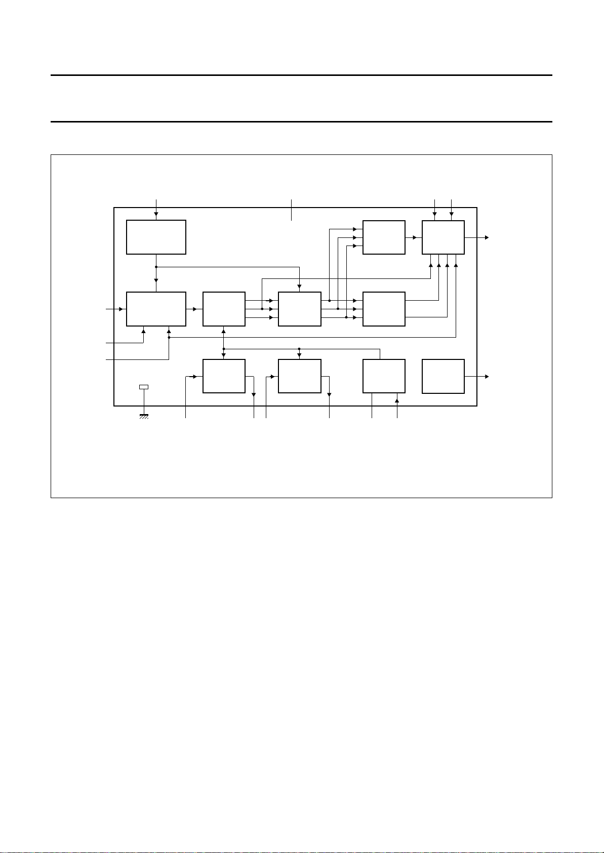
BLOCK DIAGRAM
handbook, full pagewidth
YIN
BLI/CL
AMPSEL
SC RT LW
8
SANDCASTLE
DETECTOR
BLACK
4
INSERTION
CLAMP
7
9
14 6 11 5 12 16
TDA9176
DELAY
DELAY DELAY
V
CC
CLAMPS
Fig.1 Block diagram.
2315
LTI
CONTROL
MINMAX
PTAT
CURRENT
SOURCE
R
UOUTVOUT UINVINGND
ext
f
SEL
SHAPER
BAND GAP
1
LTI
13
10
MBE775
YOUT
V
ref
1996 Jan 30 3
Philips Semiconductors Preliminary specification
Luminance Transient Improvement (LTI) IC TDA9176
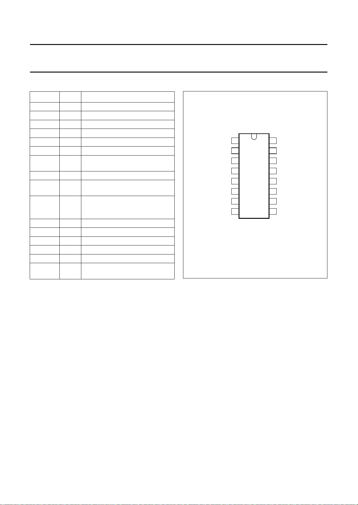
PINNING
SYMBOL PIN DESCRIPTION
f
SEL
LW 2 vertical line width control input
RT 3 rise time control input
YIN 4 luminance signal input
UIN 5 U input (colour difference signal)
VIN 6 V input (colour difference signal)
BLI/CL 7 black level insertion/clamp mode
SC 8 synchronization input signal
AMPSEL 9 high/low amplitude luminance
V
ref
VOUT 11 V output (colour difference signal)
UOUT 12 U output (colour difference signal)
YOUT 13 luminance signal output
GND 14 ground (0 V)
V
CC
R
ext
1 1FH or 2FH mode selection
selection
signal mode selection
10 internally generated reference
voltage for line width control and
rise time control
15 supply voltage (+8 V)
16 external resistor for PTAT current
source
handbook, halfpage
f
1
SEL
2
LW
3
RT
YIN
4
TDA9176
5
UIN UOUT
VIN
6
7
BLI/CL
8
SC AMPSEL
16
15
14
13
12
11
10
9
MBE776
Fig.2 Pin configuration.
R
ext
V
CC
GND
YOUT
VOUT
V
ref
1996 Jan 30 4
Philips Semiconductors Preliminary specification
Luminance Transient Improvement (LTI) IC TDA9176
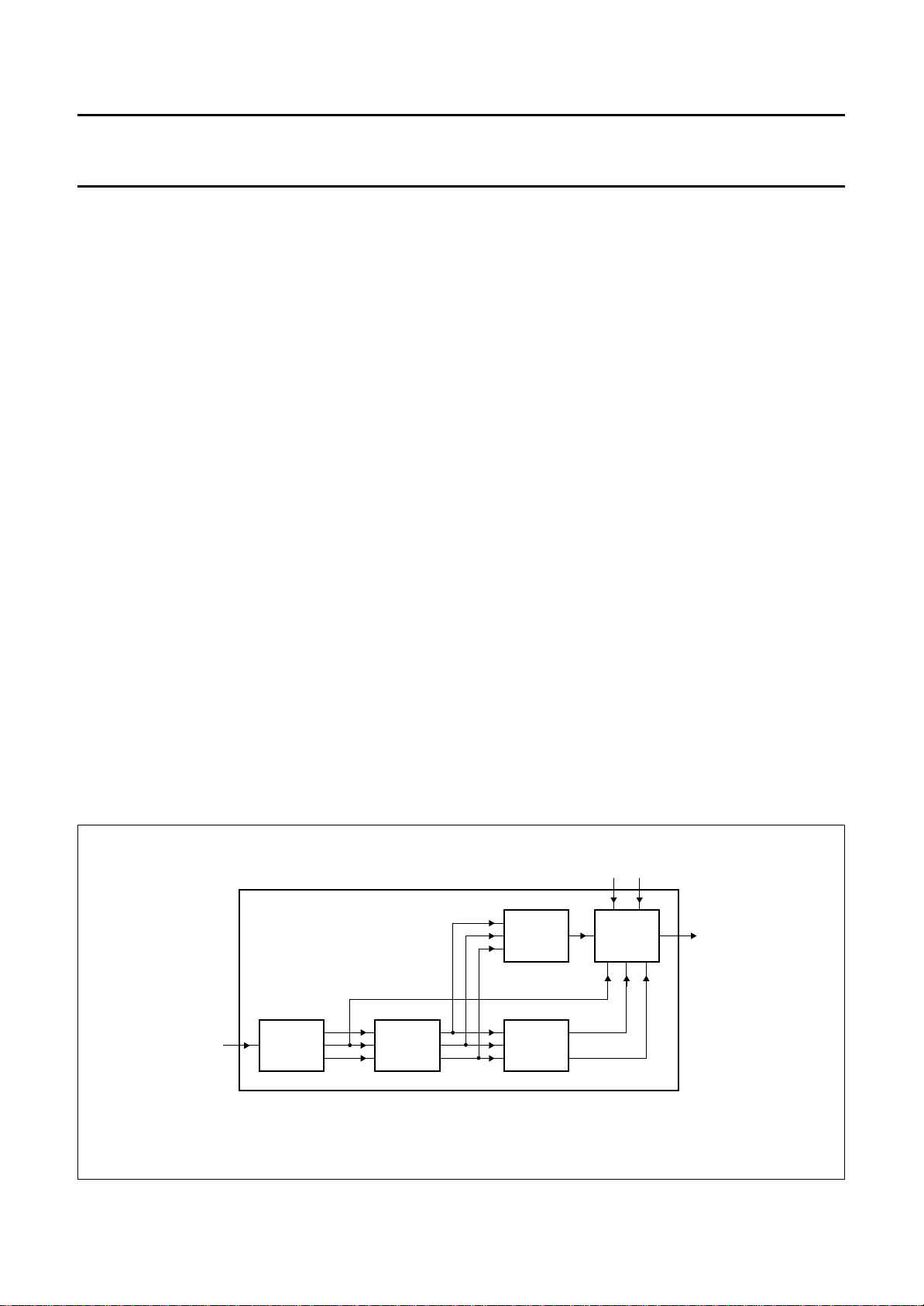
FUNCTIONAL DESCRIPTION
The TDA9176 is a Luminance Transient Improvement
(LTI) IC which is suitable for operation in both
50 and 100 Hz environments. The IC also contains
chrominance delay lines to compensate for the luminance
delay. A diagram of the LTI processor is illustrated in Fig.3.
The LTI processor contains a delay line which drives a
minimum/maximum (MINMAX) detector and a control
circuit. When the control circuit discovers a transient, the
LTI shaper switches from the minimum to the maximum
signal (or vice-versa, depending on the sign of the
transient). By mixing the original signal with the switched
signal, a variable transient improvement is obtained.
The 50% crossing point of the transient is not affected by
the LTI circuit.
If the rise time improvement is active, the duty cycle of the
output signal can be varied with the line width control input.
This function delays the rising edge and advances the
falling edge (or vice-versa). This can be used for example
aperture correction. Figures 4 and 5 illustrate some
waveforms of the LTI processor.
For correct operation the LTI circuit requires a number of
fast clamps. To overcome problems where noise is
superimposed on the input signal the device contains an
input clamp that can either clamp to the black level of the
input signal, or, insert a black level. When a black level is
inserted, the internal clamps do not respond to the noise
on the input signal (see Fig.1). When the input signal
already has an inserted black level (e.g. when it is driven
from the TDA9170 picture booster) it is recommended to
set the device to the clamping mode. If no inserted black
level is available on the input signal it is recommended to
select the black insert mode of the input clamp.
The chrominance delay lines compensate for the delay of
the luminance signal in the LTI circuit. This is to safeguard
a correct colour fit.
Two and three level sandcastles can be used as a timing
signal, only the clamp pulse of the sandcastle input is used
in the device.
There are three selection inputs to select the modes of
operation. These selections are as follows:
1. 1FH or 2FH, for the 50 or 100 Hz applications.
2. Amplitude selection, for optimum operation of the
circuit with 450 mV (p-p) or 1 V
luminance signals.
bl-wh
3. Black insertion or clamping of the luminance signal.
The selection inputs must be directly connected to either
ground or the supply rail. The modes are selected as
follows:
Frequency selection: GND = 1FH mode,
VCC= 2FH mode
Amplitude selection: GND = 450 mV (p-p),
VCC=1V
bl-wh
mode
Black insertion/clamp: GND = clamp mode,
VCC= black insert mode.
If the selection pins are left floating, internal 1 MΩ resistors
connected to the pins set the device to, 1FH mode, black
insert mode and 1 V
bl-wh
mode.
handbook, full pagewidth
YIN
1996 Jan 30 5
RT LW
23
LTI
TDA9176
4
DELAY
CLAMPS MINMAX
CONTROL
SHAPER
LTI
13
MBE777
YOUT
Fig.3 Block diagram of the LTI circuit.
 Loading...