

Philips TDA9160A-N3 Datasheet

DATA SH EET
Preliminary specification
File under Integrated Circuits, IC02
December 1991
INTEGRATED CIRCUITS
TDA9160
PAL/NTSC/SECAM decoder/sync
processor

December 1991 2
Philips Semiconductors Preliminary specification
PAL/NTSC/SECAM decoder/sync processor TDA9160
FEATURES
• Multistandard PAL, NTSC and
SECAM
• I2C-bus controlled
• I2C-bus addresses can be selected
by hardware
• Alignment free
• Few external components
• Designed for use with baseband
delay lines
• Integrated video filters
• Horizontal and vertical drive output
• East-West correction drive output
• Two CVBS inputs
• S-VHS input
• Vertical divider system
• HA synchronization pulse
• Two level sandcastle pulse
GENERAL DESCRIPTION
The TDA9160 is an I2C-bus
controlled, alignment-free
PAL/NTSC/SECAM
decoder/processor. The device
contains horizontal and vertical drive
outputs and an east-west correction
drive circuit. The TDA9160 has been
designed for use with baseband
chrominance delay lines and
DC-coupled vertical and east-west
output circuits.
The device has three inputs, two for
CVBS and one for S-VHS. The main
signal is available at the luminance
and colour difference outputs and,
also, at the TXT output
(unprocessed). The signal at the PIP
output can be selected independently
from the main signal.
The circuit provides a drive pulse for
the horizontal output stage, a
differential sawtooth current for the
vertical output stage and an east-west
drive current for the EW output stage.
These signals can be used to provide
geometry correction of the picture. A
two level sandcastle pulse and an H
A
pulse are made available for
synchronization purposes
.The I2C-bus address of the TDA9160
can be programmed by hardware.
Fig.1 Block diagram.
December 1991 3
Philips Semiconductors Preliminary specification
PAL/NTSC/SECAM decoder/sync processor TDA9160
QUICK REFERENCE DATA
ORDERING INFORMATION
Note
1. SOT232-1; 1996 December 2.
SYMBOL PARAMETER CONDITIONS MIN. TYP. MAX. UNIT
V
CC
positive supply voltage 7.2 8.0 8.8 V
I
CC
supply current − 50 − mA
V
24,26(p-p)
CVBS input voltage (peak-to-peak value) − 1.0 − V
V
23(p-p)
S-VHS luminance input voltage (peak-to-peak value) − 1.0 − V
V
22(p-p)
S-VHS chrominance burst input voltage (peak-to-peak
value)
− 0.3 − V
V
1(p-p)
luminance output voltage (peak-to-peak value) − 0.45 − V
V
25(p-p)
teletext output voltage (peak-to-peak value) − 1.0 − V
V
2(p-p)
chrominance output voltage −(R-Y) (peak-to-peak value) PAL/NTSC − 525 − mV
V
2(p-p)
chrominance output voltage −(R-Y) (peak-to-peak value) SECAM − 1.05 − V
V
3(p-p)
chrominance output voltage −(B-Y) (peak-to-peak value) PAL/NTSC − 665 − mV
V
3(p-p)
chrominance output voltage −(B-Y) (peak-to-peak value) SECAM − 1.33 − V
V
10
HA output voltage − 5.0 − V
I
15,16(p-p)
vertical drive output current (peak-to-peak value) − 1 − mA
I
18
horizontal drive output current −−10 mA
I
17
EW drive output current −−0.9 mA
V
6
sandcastle clamping voltage level − 4.5 − V
V
6
sandcastle blanking voltage level − 2.5 − V
EXTENDED TYPE
NUMBER
PACKAGE
PINS PIN POSITION MATERIAL CODE
TDA9160 32 SDIL plastic SOT232
(1)
December 1991 4
Philips Semiconductors Preliminary specification
PAL/NTSC/SECAM decoder/sync processor TDA9160
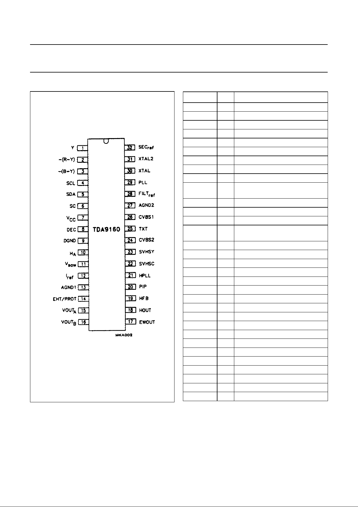
Fig.2 Pin configuration.
PINNING
SYMBOL PIN DESCRIPTION
Y 1 luminance output
−(R-Y) 2 chrominance output
−(B-Y) 3 chrominance output
SCL 4 serial clock input
SDA 5 serial data input/output
SC 6 sandcastle output
V
CC
7 positive supply input
DEC 8 positive supply decoupling
DGND 9 digital ground
H
A
10 horizontal acquisition
synchronization pulse
V
saw
11 vertical sawtooth
I
ref
12 input current reference
AGND1 13 analog ground
EHT/PROT 14 EHT tracking and over-voltage
protection
VOUT
A
15 vertical drive output A
VOUT
B
16 vertical drive output B
EWOUT 17 east-west drive output
HOUT 18 horizontal drive output
HFB 19 horizontal flyback input
PIP 20 picture-in-picture output
HPLL 21 horizontal PLL filter
SVHSC 22 S-VHS chrominance input
SVHSY 23 S-VHS luminance input
CVBS2 24 CVBS2 input
TXT 25 teletext output
CVBS1 26 CVBS1 input
AGND2 27 analog ground
FILT
ref
28 filter reference decoupling
PLL 29 colour PLL filter
XTAL 30 reference crystal input
XTAL2 31 second crystal input
SEC
ref
32 SECAM reference decoupling

December 1991 5
Philips Semiconductors Preliminary specification
PAL/NTSC/SECAM decoder/sync processor TDA9160
FUNCTIONAL DESCRIPTION
The TDA9160 is an I2C-bus
controlled, alignment free
PAL/NTSC/SECAM colour
decoder/sync processor/deflection
controller which has been designed
for use with baseband chrominance
delay lines.
In the standard operating mode the
I2C-bus address is 8A . If the TXT
output is connected to the positive rail
the address will change to 8E
The standards which the TDA9160
can decode are dependent on the
choice of external crystals. If a
4.4 MHz and a 3.6 MHz crystal are
used then SECAM, PAL 4.4/3.6 and
NTSC 4.4/3.6 can be decoded. If two
3.6 MHz crystals are used then only
PAL 3.6 and NTSC 3.6 can be
decoded. Which 3.6 MHz standards
can be decoded is dependent on the
exact frequencies of the crystal. In an
application where not all standards
are required only one crystal is
sufficient (in this instance the crystal
must be connected to the reference
crystal input (pin 30)). If a 4.4 MHz
crystal is used it must always be
connected to pin 30. Both crystals are
used to provide a reference for the
filters and the horizontal PLL,
however, only the reference crystal is
used to provide a reference for the
SECAM demodulator.
To enable the calibrating circuits to be
adjusted exactly two bits from the
I2C-bus address are used to indicate
which crystals are connected to the
IC.
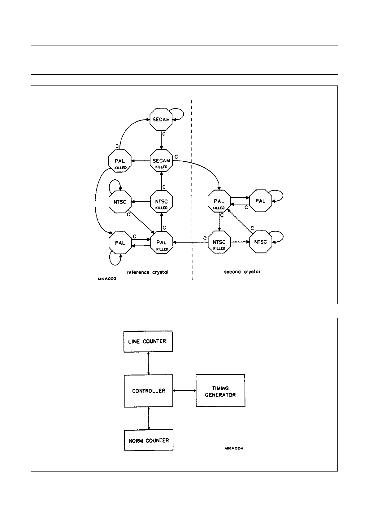
The standard identification circuit is a
digital circuit without external
components; the search loop is
illustrated in Fig.3.
The decoder (via the I2C-bus) can be
forced to decode either SECAM or
PAL/NTSC (but not PAL or NTSC).
Crystal selection can also be forced.
Information, concerning which
standard and which crystal have been
selected and whether the colour killer
is ON or OFF is provided by the read
out. Using the forced-mode does not
affect the search loop, it does,
however, prevent the decoder from
reaching or staying in an unwanted
state. The identification circuit skips
impossible standards (e.g. SECAM
when no 4.4 MHz crystal is fitted) and
illegal standards (e.g. forced mode).
To reduce the risk of wrong
identification PAL has priority over
SECAM (only line identification is
used for SECAM).
The TDA9160 has two CVBS inputs
and one S-VHS input which can be
selected via the I
2
C-bus. The input
selector can also be switched to
enable CVBS2 to be processed,
providing that there is no S-VHS
signal present at the input. If the input
selector is set to CVBS2 it will switch
to S-VHS if an S-VHS sync pulse is
detected at the luminance input. The
S-VHS detector output can be read
via the I2C-bus.
If the voltage at either the S-VHS
luminance or the chrominance input
(pins 22 and 23) exceeds +5.5 V the
IC will revert to test mode.
The TDA9160 also provides outputs
for picture-in-picture and teletext (PIP
pin 20 and TXT pin 25). The decoder
input signal can be switched directly
to the TXT output. The PIP output
signal can be selected independently
from the TXT output. If S-VHS is
selected at the TXT output only the
luminance signal will be present; if
S-VHS is selected at the PIP output
then the luminance and chrominance
signals will be added.
All filters, including the luminance
delay line, are an integral part of the
IC. The filters are gyrator-capacitor
type filters. The resonant frequency of
the filters is controlled by a circuit that
uses the active crystal to tune the
SECAM Cloche filter during the
vertical flyback time. The remaining
filters and the delay line are matched
to this filter. The filters can be
switched to either 4.43 MHz,
4.28 MHz or 3.58 MHz irrespective of
the frequency of the active crystal.
The switching is controlled by the
identification circuit.
The S-VHS luminance signal does
not pass through the notch filter to
preserve bandwidth. The luminance
delay line delivers the Y signal to the
output 40 ns after the −(R-Y) and
−(B-Y) signals. This compensates for
the delay of the external chrominance
delay lines.
The PAL/NTSC demodulator
employs an oscillator that can operate
with either crystal (3.6 or 4.4 MHz). If
the I2C-bus indicates that only one
crystal is connected it will always
connect to the crystal at the reference
input (pin 30).
The Hue signal, which is adjustable
via the I2C-bus, is gated during the
burst for NTSC signals.
The SECAM demodulator is an
auto-calibrating PLL demodulator
which has two references. The
reference crystal, to force the PLL to
the desired free-running frequency
and the bandgap reference, to obtain
the correct absolute value of the
output signal. The VCO of the PLL is
calibrated during each vertical flyback
period, when the reference crystal is
active. When the second crystal is
active the VCO is not calibrated.
During this time the frequency of the
VCO is kept constant by applying a
constant voltage to its control input. If
the reference crystal is not 4.4 MHz
the decoder will not produce the
correct SECAM signals.
The main part of the sync circuit is a
432 × fH (6.75 MHz) oscillator the
frequency of which is divided by 432

December 1991 6
Philips Semiconductors Preliminary specification
PAL/NTSC/SECAM decoder/sync processor TDA9160
to lock the phase 1 loop to the
incoming signal. The time constant of
the loop can be forced by the I2C-bus
(fast or slow). If required the IC can
select the time constant, depending
on the noise content of the input
signal and whether the loop is phase
locked or not (medium or slow). The
free-running frequency of the
oscillator is determined by a digital
control circuit that is locked to the
active crystal.
When a power-on-reset pulse is
detected the frequency of the
oscillator is switched to a frequency
greater than 6.75 MHz to protect the
horizontal output transistor. The
oscillator frequency is reset to
6.75 MHz when the crystal indication
bits have been loaded into the IC. To
ensure that this procedure does not
fail it is absolutely necessary to send
subaddress 00 before subaddress
01. Subaddress 00 contains the
crystal indication bits, when
subaddress 01 is received the line
oscillator calibration will be initiated.
The calibration is terminated when
the oscillator frequency reaches
6.75 MHz. The oscillator is again
calibrated when an out-of-lock
condition with the input signal is
realised by the coincidence detector.
Again the calibration will be
terminated when the oscillator
frequency reaches 6.75 MHz.
The phase 1 loop can be opened
using the I2C-bus. This is to facilitate
On Screen Display (OSD)
information. If there is no input signal
or a very noisy input signal the phase
1 loop can be opened to provide a
stable line frequency and thus a
stable picture.
The sync part provides an HA pulse
that is coupled to the processed
CVBS signal.
The horizontal drive signal can be
switched off via the I2C-bus (standby
mode). The horizontal drive is also
switched off when the over-voltage
protection circuit trips or when a POR
is detected. Should either of these
two conditions occur the IC will return
to the normal operating mode when
the appropriate command is received
via the I2C-bus. The duty cycle of the
horizontal drive signal is increased
from 2%, at start-up, to a constant
value of 55% in approximately 300
lines. The two-level sandcastle pulse
provides a combined horizontal and
vertical blanking signal and a
clamping pulse coupled to the display
section of the TV.
The vertical sawtooth generator
drives the geometry processing
circuits which provide control for the
horizontal shift, EW width, EW
parabola/width ratio, EW
corner/parabola ratio, trapezium
correction, vertical slope, vertical
shift, vertical amplitude and the
S-correction. All of these control
functions can be set via the I2C-bus.
The geometry processor has a
differential current output for the
vertical drive signal and a
single-ended output for the EW drive.
Both the vertical drive and the EW
drive outputs can be modulated for
EHT compensation. The EHT
compensation pin (pin 14) can also be
used for over-voltage protection.
De-interlace of the vertical output can
be set via the I2C-bus.
The vertical divider system has a fully
integrated vertical sync separator.
The divider can accommodate both
50 and 60 Hz systems; it can either
locate the field frequency
automatically or it can be forced to the
desired system via the I2C-bus. A
block diagram of the vertical divider
system is illustrated in Fig.4. The
divider system operates at 432 times
the horizontal line frequency. The line
counter receives enable pulses at
twice the line frequency, thereby
counting two lines per pulse.
A state diagram of the controller is
illustrated in Fig.5. Because it is
symmetrical only the right hand part
will be described.
Depending on the previously found
field frequency, the controller will be
in one of the 'count' states. When the
line counter has counted 488 pulses
(i.e. 244 lines of the video input
signal) the controller will move to the
next state depending on the output of
the norm counter. This can be either
NORM, NEAR-NORM or NO-NORM
depending on the position of the
vertical sync pulse in the previous
fields. When the counter is in the
NORM state it generates the vertical
sync pulse (VSP) automatically and
then, when the line counter is at
LC = 626, moves to the WAIT state.
In this condition it waits for the next
pulse of the double line frequency
signal and then moves to the COUNT
state of the current field frequency.
When the controller returns to the
COUNT state the line counter will be
reset half a line after the start of the
vertical sync pulse of the video input
signal.
When the controller is in the
NEAR-NORM state it will move to the
COUNT state if it detects the vertical
sync pulse within the NEAR-NORM
window (i.e. 622 < LC < 628). If no
vertical sync pulse is detected, the
controller will move back to the
COUNT state when the line counter
reaches LC = 628. The line counter
will then be reset.
When the controller is in the
NO-NORM state it will move to the
COUNT state when it detects a
vertical sync pulse and reset the line
counter. If a sync pulse is not
detected before LC = 722 (if the
phase loop is locked in forced mode)
it will move to the COUNT state and
reset the line counter. If the phase
loop is not locked the controller will
move back to the COUNT state when
LC = 628. The forced mode option
keeps the controller in either the
left-hand side (60 Hz) or the
December 1991 7
Philips Semiconductors Preliminary specification
PAL/NTSC/SECAM decoder/sync
processor
TDA9160
right-hand side (50 Hz) of the state
diagram.
Figure 6 illustrates the state diagram
of the 'norm' counter which is an
up/down counter that counts up if it
finds a vertical sync pulse within the
selected window. In the
NEAR-NORM and NORM states the
first correct vertical sync pulse after
one or more incorrect vertical sync
pulses is processed as an incorrect
pulse. This procedure prevents the
system from staying in the
NEAR-NORM or NORM state if the
vertical sync pulse is correct in the
first field and incorrect in the second
field. If no vertical sync pulse is found
in the selected window this will always
result in a down pulse for the 'norm'
counter.
Figure 7 illustrates the timing of the
display sandcastle (DSC) and the
reset pulse of the vertical sawtooth
with respect to the input signal
I
2
C-bus protocol
If the TXT output is connected to the
positive supply the address will
change from 8A to 8E.
Valid subaddresses = 00 to 0F
Auto-increment mode available for
subaddresses.
Subaddress 00 must always be sent
before subaddress 01 in order to
protect the horizontal output
transistor.
Table 1 Slave address (8A)
Table 2 Inputs
Table 3 Outputs
A6 A5 A4 A3 A2 A1 A0 R/
W
10001X1X
SUBADDRESS MSB LSB
00 INA INB INC IND FOA FOB XA XB
01 FORF FORS DL STB POC FM SAF FRQF
02 −−HU5 HU4 HU3 HU2 HU1 HU0
03 −−HS5 HS4 HS3 HS2 HS1 HS0
04 −−EW5 EW4 EW3 EW2 EW1 EW0
05 −−PW5 PW4 PW3 PW2 PW1 PW0
06 −−CP5 CP4 CP3 CP2 CP1 CP0
07 −−TC5 TC4 TC3 TC2 TC1 TC0
08 −−VS5 CS4 VS3 VS2 VS1 VS0
09 −−VA5VA4VA3VA2VA1VA0
0A −−SC5 SC4 SC3 SC2 SC1 SC0
0B SBL − VSH5 VSH4 VSH3 VSH2 VSH1 VSH0
ADDRESS POR FSI STS SL PROT SAK SBK FRQ
December 1991 8
Philips Semiconductors Preliminary specification
PAL/NTSC/SECAM decoder/sync processor TDA9160
Fig.3 Search loop of the identification circuit.
Fig.4 Block diagram of the vertical divider system.

December 1991 9
Philips Semiconductors Preliminary specification
PAL/NTSC/SECAM decoder/sync processor TDA9160
Fig.5 State diagram of the vertical divider system.
Fig.6 State diagram of the ‘norm’ counter.
 Loading...