

Philips tda9151b DATASHEETS

INTEGRATED CIRCUITS
DATA SH EET
TDA9151B
Programmable deflection controller
Preliminary specification
Supersedes data of June 1993
File under Integrated Circuits, IC02
Philips Semiconductors
July 1994

Philips Semiconductors Preliminary specification
Programmable deflection controller TDA9151B
FEATURES
General
• 6.75, 13.5 and 27 MHz clock frequency
• Few external components
• Synchronous logic
2
• I
C-bus controlled
• Easy interfacing
• Low power
• ESD protection
• Flash detection with restart
• Two-level sandcastle pulse.
Vertical deflection
• 16-bit precision vertical scan
• Self adaptive or programmable fixed slope mode
• DC coupled deflection to prevent picture bounce
• Programmable fixed compression to 75%
• Programmable vertical expansion in the fixed slope
mode
• S-correction can be preset
• S-correction setting independent of the field frequency
• Differential output for high DC stability
• Current source outputs for high EMC immunity
• Programmable de-interlace phase.
East-West correction
• DC coupled EW correction to prevent picture bounce
• 2nd and 4th order geometry correction can be preset
• Trapezium correction
• Geometry correction settings are independent of field
frequency
• Self adaptive Bult generator prevents ringing of the
horizontal deflection
• Current source output for high EMC immunity.
Horizontal deflection
• Phase 2 loop with low jitter
• Internal loop filter
• Dual slicer horizontal flyback input
2
• Soft start by I
C-bus
• Over voltage protection/detection with selection and
status bit.
EHT correction
• Input selection between aquadag or EHT bleeder
• Internal filter.
GENERAL DESCRIPTION
The TDA9151B is a programmable deflection controller
contained in a 20-pin DIP package and constructed using
BIMOS technology. This high performance
synchronization and DC deflection processor has been
especially designed for use in both digital and analog
based TV receivers and monitors, and serves horizontal
and vertical deflection functions for all TV standards. The
TDA9151B uses a line-locked clock at 6.75, 13.5 or
27 MHz, depending on the line frequency and application,
and requires only a few external components. The device
can be programmed in a self-adaptive mode or in a
programmable fixed slope mode. Selection of these
modes and a large number of other functions is fully
2
programmable via the I
C-bus.
ORDERING INFORMATION
TYPE NUMBER
TDA9151B 20 DIP plastic SOT146-1
July 1994 2
PACKAGE
PINS PIN POSITION MATERIAL CODE

Philips Semiconductors Preliminary specification
Programmable deflection controller TDA9151B
QUICK REFERENCE DATA
SYMBOL PARAMETER CONDITIONS MIN. TYP. MAX. UNIT
V
CC
I
CC
P
tot
T
amb
Inputs
V
14
V
13
V
12
V
5
V
18
V
17
V
1
V
1
V
3
V
9
Outputs
V
20
I
11−I10(M)
V
10,11
I
6(M)
V
6
SANDCASTLE OUTPUT LEVELS (DSC)
V
2
V
2
V
2
HORIZONTAL OFF-CENTRE SHIFT (OFCS)
V
19
supply voltage 7.2 8.0 8.8 V
supply current f
= 6.75 MHz − 27 − mA
clk
total power dissipation − 220 − mW
operating ambient temperature −25 − +70 °C
line-locked clock (LLC) logic level − TTL −
horizontal sync (HA) logic level − TTL −
vertical sync (VA) logic level − TTL −
line-locked clock select (LLCS)
note 1 − CMOS 5 V −
logic level
serial clock (SCL) logic level − CMOS 5 V −
serial data input (SDA) logic level − CMOS 5 V −
horizontal flyback (HFB) phase
slicing level
horizontal flyback (HFB) blanking
FBL = logic 0 − 3.9 − V
FBL = logic 1 − 1.3 − V
− 100 − mV
slicing level
over voltage protection (PROT)
− 3.9 − V
level
EHT flash detection level − 1.5 − V
horizontal output (HOUT) voltage
I20 = 10 mA −− 0.5 V
(open drain)
vertical differential (VOUT
output current (peak value)
A, B
)
vertical amplitude = 100%;
I8 = −120 µA; note 2
440 475 510 µA
vertical output voltage 0 − 3.9 V
EW (EWOUT) total output current
I8 = −120 µA −− 930 µA
(peak value)
EW (EWOUT) output voltage 1.0 − 5.5 V
base voltage level − 0.5 − V
horizontal and vertical blanking
− 2.5 − V
voltage level
video clamping voltage level − 4.5 − V
output voltage I19 = 2 mA 0 − V
CC
V
Notes
1. Hard wired to ground or V
2. DAC values: vertical amplitude = 31; EHT = 0; SHIFT = 3; SCOR = 0.
July 1994 3
is highly recommended.
CC
Philips Semiconductors Preliminary specification
Programmable deflection controller TDA9151B
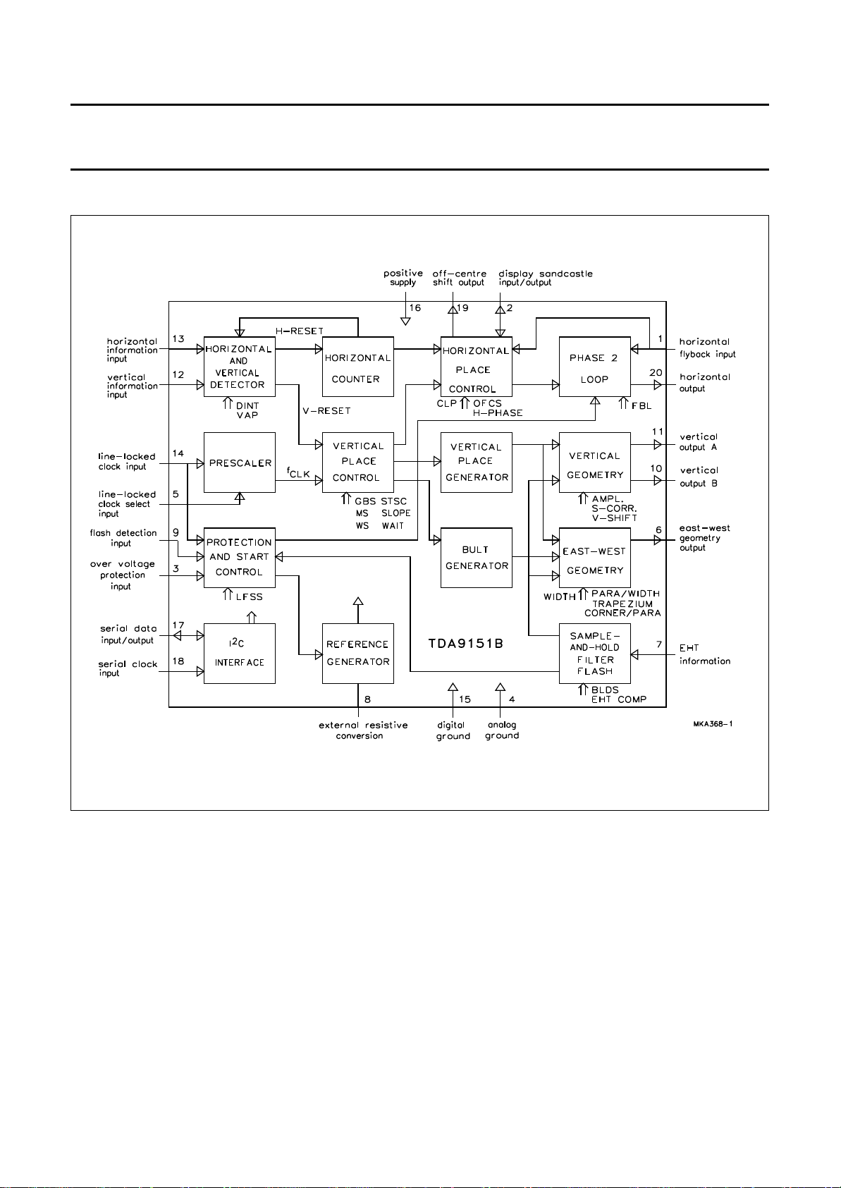
BLOCK DIAGRAM
July 1994 4
Fig.1 Block diagram.
Philips Semiconductors Preliminary specification
Programmable deflection controller TDA9151B
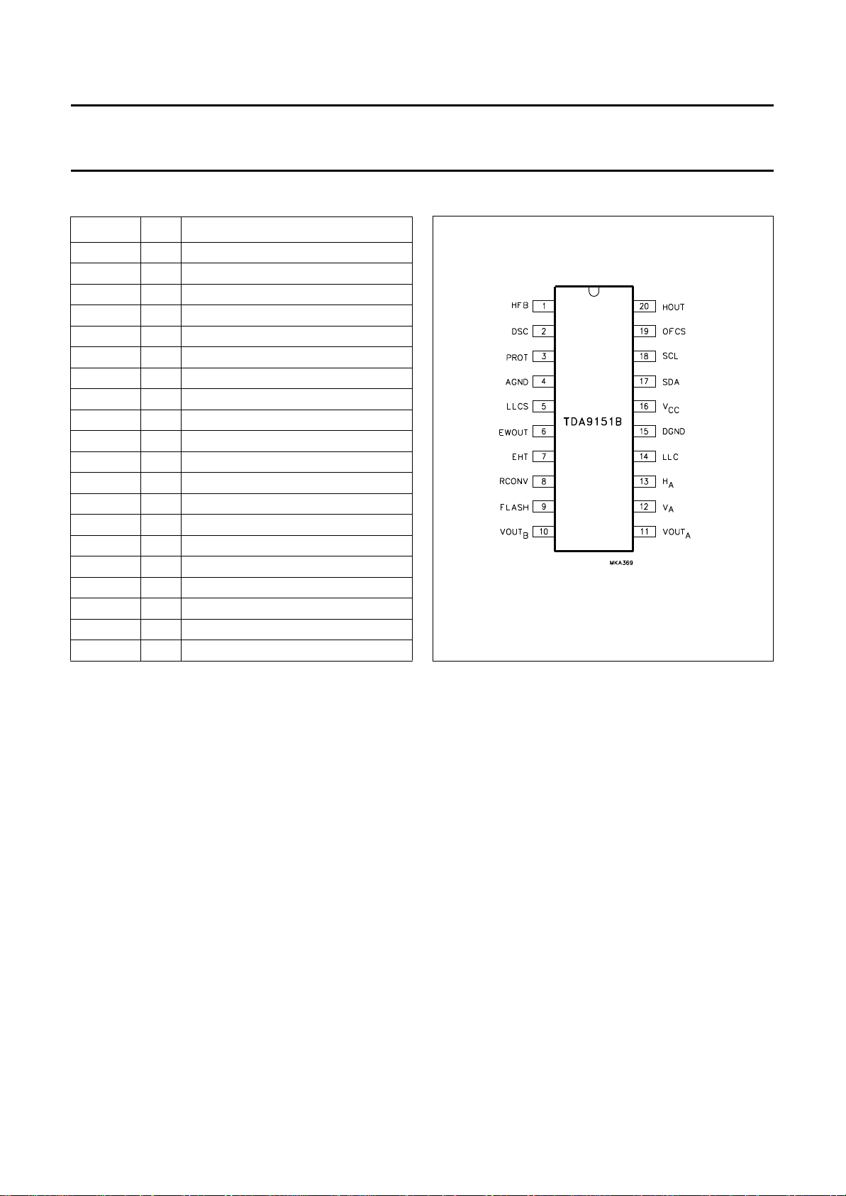
PINNING
SYMBOL PIN DESCRIPTION
HFB 1 horizontal flyback input
DSC 2 display sandcastle input/output
PROT 3 over voltage protection input
AGND 4 analog ground
LLCS 5 line-locked clock selection input
EWOUT 6 east-west geometry output
EHT 7 EHT compensation
R
CONV
FLASH 9 flash detection input
VOUT
B
VOUT
A
V
A
H
A
LLC 14 line-locked clock input
DGND 15 digital ground
V
CC
SDA 17 serial data input/output
SCL 18 serial clock input
OFCS 19 off-centre shift output
HOUT 20 horizontal output
8 external resistive conversion
10 vertical output B
11 vertical output A
12 vertical information input
13 horizontal information input
16 supply input (+8 V)
Fig.2 Pin configuration.
FUNCTIONAL DESCRIPTION
Input signals (pins 12, 13, 14, 17 and 18)
The TDA9151B requires three signals for minimum
operation (apart from the supply). These signals are the
line-locked clock (LLC) and the two I
2
C-bus signals (SDA
and SCL). Without the LLC the device will not operate
because the internal synchronous logic uses the LLC as
the system clock.
I2C-bus transmissions are required to enable the device to
perform its required tasks. Once started the IC will use the
HA and/or VA inputs for synchronization. If the LLC is not
July 1994 5
present the outputs will be switched off and all operations
discarded (if the LLC is not present the line drive will be
inhibited within 2 µs, the EW output current will drop to
zero and the vertical output current will drop to 20% of the
adjusted value within 100 µs). The SDA and SCL inputs
meet the I2C-bus specification, the other three inputs are
TTL compatible.
The LLC frequency can be divided-by-two internally by
connecting LLCS (pin 5) to ground thereby enabling the
prescaler.
The LLC timing is given in the Chapter “Characteristics”.

Philips Semiconductors Preliminary specification
Programmable deflection controller TDA9151B
I2C-bus commands
Slave address: 8C HEX = 1000110X BIN
READ MODE
The format of the status byte is: PON PROT 000000
Where:
PON is the status bit for power-on reset (POR) and after
power failure:
• Logic 1:
– after the first POR and after power failure; also set to
1 after a severe voltage dip that may have disturbed
the various settings
– POR 1 to 0 transition, VCC = 6.25 V (typ.)
– POR 0 to 1 transition, VCC = 5.75 V (typ.)
Table 1 Write mode with auto increment; subaddress and data byte format.
FUNCTION SUBADDRESS
Vertical amplitude 00 X
Vertical S-correction 01 X X A5 A4 A3 A2 A1 A0
Vertical start scan 02 X X A5 A4 A3 A2 A1 A0
Vertical off-centre shift 03 X note 2 note 2 note 2 X A2 A1 A0
EW trapezium correction 03 X A6 A5 A4 X note 2 note 2 note 2
EW width/width ratio 04 X X A5 A4 A3 A2 A1 A0
EW parabola/width ratio 05 X X A5 A4 A3 A2 A1 A0
EW corner/parabola ratio 06 X X A5 A4 A3 A2 A1 A0
EHT compensation 07 X X A5 A4 A3 A2 A1 A0
Horizontal phase 08 X X A5 A4 A3 A2 A1 A0
Horizontal off-centre shift 09 X X A5 A4 A3 A2 A1 A0
Clamp shift 0A X XXXXA2A1A0
Control 1 0B MS WS FBL VAP BLDS LFSS DINT GBS
Vertical slope MSB 0C A7 A6 A5 A4 A3 A2 A1 A0
Vertical slope LSB 0D A7 A6 A5 A4 A3 A2 A1 A0
Vertical wait 0E A7 A6 A5 A4 A3 A2 A1 A0
Control 2 0F X X X VPR CPR DIP PRD CSU
D7 D6 D5 D4 D3 D2 D1 D0
(1)
• Logic 0:
– after a successful read of the status byte.
PROT is the over voltage detection for the scaled EHT
input:
• Logic 1:
– if the scaled EHT rises above the reference value of
3.9 V
• Logic 0:
– after a successful read of the status byte and EHT
<3.9 V.
Remark: a read action is considered successful when an
End Of Data signal has been detected (i.e. no master
acknowledge).
DATA BYTE
X A5A4A3A2A1A0
Notes
1. X = don’t care.
2. Data bit used in another function.
July 1994 6

Philips Semiconductors Preliminary specification
Programmable deflection controller TDA9151B
Table 2 Control bits.
CONTROL BIT LOGIC FUNCTION
LFSS 0 Line stop: EW output current becomes zero and the vertical output current is reduced
to 20% of the adjusted value. LFSS becomes logic 0 after a HIGH on PON.
1 Line start enabled: the soft start mechanism is now activated.
DINT 0 De-interlace on: the V
1 De-interlace off: the V
edge is used as vertical reset.
BLDS 0 Aquadag selected.
1 Bleeder selected.
GBS 0 Becomes logic 0 after power-on.
1 Guard band 48/12 lines.
VAP 0 Positive V
1 Negative V
edge detection.
A
edge detection.
A
FBL 0 Horizontal flyback slicing level = 3.9 V.
1 Horizontal flyback slicing level = 1.3 V.
WS 0 No wait state.
1 Programmable wait state (only in constant slope mode; MS = logic 1).
MS 0 Adaptive mode with guardband amplitude control.
1 Constant slope mode (programmable).
CSU 0 No clamping suppression, standard mode of operation.
1 Clamping suppression in wait, stop and protection modes
(used in systems with e.g. TDA4680/81).
PRD 0 No defeat of HOUT, the over voltage information is only written in the PROT status bit.
1 HOUT is defeated and status bit PROT is set when over voltage is detected.
DIP 0 V
1V
is sampled 42 clock pulses after the leading edge of HA.
A
is sampled 258 clock pulses after the leading edge of HA.
A
CPR 0 Nominal amplitude.
1 Compression to 75% of adjusted amplitude, used for display of 16 : 9 standard pictures
on 4 : 3 displays.
VPR 0 Nominal amplitude (100%) during wait, stop and clipping.
1 Amplitude reduced to 20% during wait, stop and clipping.
pulse is sampled at a position selected with control bit DIP.
A
pulse is sampled with the system clock and the detected rising
A
July 1994 7
Philips Semiconductors Preliminary specification
Programmable deflection controller TDA9151B
Table 3 Explanation of control bits shown in Table 2.
CONTROL BITS DESCRIPTION
LFSS line frame start/stop
DINT de-interlace
BLDS bleeder mode selection
GBS guard band selection
VAP polarity of V
FBL flyback slicing level
WS wait state on/off
MS mode select
CSU clamping suppression mode
PRD protection/detection mode
DIP de-interlace phase
CPR compression on/off
VPR vertical power reduction mode
edge detection
A
Table 4 Clock frequency control bit (pin 5; note 1).
CONTROL BIT LOGIC FUNCTION
LLCS 0 prescaler on: the internal clock frequency f
1 prescaler off (default by internal pull-up resistor): the internal clock frequency f
clk
=1⁄2f
LLC
clk=fLLC
Note
1. Switching of the prescaler is only allowed when LFSS is LOW. It is highly recommended to hard wire LLCS to ground
. Active switching may damage the output power transistor due to the changing HOUT pulse. This may cause
or V
CC
very high currents and large flyback pulses. The permitted combinations of LLC and the prescaler are shown in
Table 5.
Table 5 Line duration with prescaler.
LLC (MHz) ON (µs) OFF (µs)
6.75 note 1 64
13.5 64 32
27 32 note 1
Note
1. Combination not allowed.
July 1994 8
Philips Semiconductors Preliminary specification
Programmable deflection controller TDA9151B
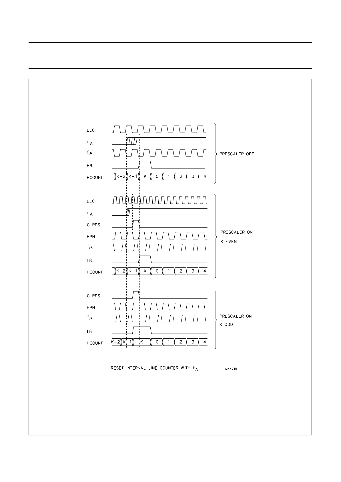
July 1994 9
Fig.3 Timing relations between LLC, HA and line counter.

Philips Semiconductors Preliminary specification
Programmable deflection controller TDA9151B
Horizontal part (pins 1, 2, 13, 19 and 20
S
YNCHRONIZATION PULSE
The HA input (pin 13) is a TTL-compatible CMOS input.
Pulses on this input have to fulfil the timing requirements
as illustrated in Fig.6. For correct detection the minimum
pulse width for both the HIGH and LOW periods is 2
internal clock periods.
F
LYBACK INPUT PULSE
The HFB input (pin 1) is a CMOS input. The delay of the
centre of the flyback pulse to the leading edge of the H
A
pulse can be set via the I2C-bus with the horizontal phase
byte (subaddress 08), as illustrated in Fig.7.
The resolution is 6-bit.
UTPUT PULSE
O
The HOUT pulse (pin 20) is an open-drain NMOS output.
The duty factor for this output is typically52⁄
48
(conducting/non-conducting) during normal operation. A
soft start causes the duty factor to increase linearly from 5
to 52% over a minimum period of 2000 lines in 2000 steps.
FF-CENTRE SHIFT
O
The OFCS output (pin 19) is a push-pull CMOS output
which is driven by a pulse-width modulated DAC.
By using a suitable interface, the output signal can be used
for off-centre shift correction in the horizontal output stage.
This correction is required for HDTV tubes with a 16 × 9
aspect ratio and is useful for high performance flat square
tubes to obtain the required horizontal linearity. For
applications where off-centre correction is not required,
the output can be used as an auxiliary DAC. The OFCS
signal is phase-locked with the line frequency. The
off-centre shift can be set via the I2C-bus, subaddress 09,
with a 6-bit resolution as illustrated in Fig.8.
S
ANDCASTLE
The DSC input/output (pin 2) acts as a sandcastle
generating output and a guard sensing input. As an output
it provides 2 levels (apart from the base level), one for the
horizontal and vertical blanking and the other for the video
clamping. As an input it acts as a current sensor during the
vertical blanking interval for guard detection.
LAMPING PULSE
C
The clamping pulse width is 21 internal clock periods. The
shift, with respect to HA can be varied from 35 to 49 clock
periods in 7 steps via the I2C-bus, clamp shift byte
subaddress 0A, as illustrated in Fig.9. It is possible to
suppress the clamping pulse during wait, stop and
protection modes with control bit CSU. This will avoid
unwanted reset of the TDA4680/81 (only used in those
circuits).
H
ORIZONTAL BLANKING
The start of the horizontal blanking pulse is minimum 38
and maximum 41 clock periods before the centre of the
flyback pulse, depending on the f
clk/fH
ratio K in
accordance with 41 − (432 − K).
Stop of the horizontal blanking pulse is determined by the
trailing edge of the HFB pulse at the horizontal blanking
slicing level crossing as illustrated in Fig.10.
ERTICAL BLANKING
V
The vertical blanking pulse starts two internal clock pulses
after the rising edge of the VA pulse. During this interval a
small guard pulse, generated during flyback by the vertical
power output stage, must be inserted. Stop vertical
blanking is effected at the end of the blanking interval only
when the guard pulse is present (see Section “Vertical
guard”).
The start scan setting determines the end of vertical
blanking with a 6-bit resolution in steps of one line via the
I2C-bus subaddress 02 (see Figs 11, 12 and 13).
ERTICAL GUARD
V
In the vertical blanking interval a small unblanking pulse is
inserted. This pulse must be filled-in by a blanking pulse or
guard pulse from the vertical power output stage which
was generated during the flyback period. In this condition
the sandcastle output acts as guard detection input and
requires a minimum 800 µA input current. This current is
sensed during the unblanking period. Vertical blanking is
only stopped at the end of the blanking interval when the
inserted pulse is present. In this way the picture tube is
protected against damage in the event of missing or
malfunctioning vertical deflection (see Figs 11, 12 and 13).
July 1994 10
 Loading...