

Philips tda9143 DATASHEETS

INTEGRATED CIRCUITS
DATA SH EET
TDA9143
2
I
C-bus controlled, alignment-free
PAL/NTSC/SECAM decoder/sync
processor
Preliminary specification
File under Integrated Circuits, IC02
1996 Jan 17

Philips Semiconductors Preliminary specification
I2C-bus controlled, alignment-free
PAL/NTSC/SECAM decoder/sync processor
FEATURES
• Multi-standard colour decoder and sync processor for
PAL, NTSC and SECAM
• PALplus helper blanking and EDTV-2 blanking
• I2C-bus controlled
• I2C-bus addresses hardware selectable
• Pin compatible with TDA9141
• Alignment free
• Few external components
• Designed for use with baseband delay lines
• Integrated video filters
• Adjustable luminance delay
2
• Noise detector with I
• Norm/no_norm detector with I2C-bus read-out
• CVBS or Y/C input, with automatic detection possibility
• CVBS output, provided I2C-bus address 8A is used
• Vertical divider system
• Two-level sandcastle signal
• VA synchronization pulse (3-state)
• HA synchronization pulse or clamping pulse CLP
input/output
• Line-locked clock output (6.75 MHz or 6.875 MHz) or
stand-alone I2C-bus output port
• Stand-alone I2C-bus input/output port
• Colour matrix and fast YUV switch
• Comb filter enable input/output with subcarrier
frequency
• Internal bypass mode of external delay line for NTSC
applications
• Low power standby mode with 3-state YUV outputs
• Fast blanking detector with I2C-bus read-out
• Blanked or unblanked sync on Y
• Internal MACROVISION gating for the horizontal PLL
enabled by bus bit EMG.
C-bus read-out
out
by I2C-bus bit BSY
GENERAL DESCRIPTION
The TDA9143 is an I
PAL/NTSC/SECAM decoder/sync processor with blanking
facilities for PALplus and EDTV-2 signals. The TDA9143
has been designed for use with baseband chrominance
delay lines, and has a combined subcarrier
frequency/comb filter enable signal for communication
with a PAL/NTSC comb filter.
The IC can process both CVBS input signals and Y/C input
signals. The input signal is available on an output pin, in
the event of a Y/C signal, it is added into a CVBS signal.
The sync processor provides a two-level sandcastle, a
horizontal pulse (CLP or HA pulse, bus selectable) and a
vertical (VA) pulse. When the HA pulse is selected, a
line-locked clock (LLC) signal is available at the output port
pin (6.75 MHz or 6.875 MHz).
A fast switch can select either the internal Y signal with the
UV input signals, or YUV signals made of the RGB input
signals. The RGB input signals can be clamped with either
the internal or an external clamping signal.
Two pins with an input/output port and an output port of the
2
C-bus are available.
I
The I2C-bus address of the TDA9143 is hardware
programmable.
TDA9143
2
C-bus controlled, alignment-free
ORDERING INFORMATION
TYPE
NUMBER
TDA9143 SDIP32 plastic shrink dual in-line package; 32 leads (400 mil) SOT232-1
1996 Jan 17 2
NAME DESCRIPTION VERSION
PACKAGE
Philips Semiconductors Preliminary specification
I2C-bus controlled, alignment-free
TDA9143
PAL/NTSC/SECAM decoder/sync processor
QUICK REFERENCE DATA
SYMBOL PARAMETER CONDITIONS MIN. TYP. MAX. UNIT
V
CC
I
CC
V
CVBS(p-p)
V
Y(p-p)
V
C(p-p)
V
Y(out)
V
U(out)(p-p)
V
V(out)(p-p)
V
SC(bl)
V
SC(clamp)
V
VA
V
HA
V
LLC(p-p)
V
R,G,B(p-p)
V
clamp(I/O)
V
sub(p-p)
V
OPORT
positive supply voltage 7.2 8.0 8.8 V
supply current 50 60 70 mA
CVBS input voltage (peak-to-peak value) top sync-white − 1.0 1.43 V
luminance input voltage
top sync-white − 1.0 1.43 V
(peak-to-peak value)
chrominance burst input voltage
− 0.3 0.6 V
(peak-to-peak value)
luminance black-white output voltage − 1.0 − V
U output voltage (peak-to-peak value) standard colour bar − 1.33 − V
V output voltage (peak-to-peak value) standard colour bar − 1.05 − V
sandcastle blanking voltage level 2.2 2.5 2.8 V
sandcastle clamping voltage level 4.2 4.5 4.8 V
VA output voltage 4.0 5.0 5.5 V
HA output voltage 4.0 5.0 5.5 V
LLC output voltage amplitude
250 500 − mV
(peak-to-peak value)
RGB input voltage (peak-to-peak value) 0 to 100% saturation − 0.7 1.0 V
clamping pulse input/output voltage − 5.0 − V
subcarrier output voltage amplitude
150 200 300 mV
(peak-to-peak value)
port output voltage 4.0 5.0 5.5 V
1996 Jan 17 3
Philips Semiconductors Preliminary specification
I2C-bus controlled, alignment-free
PAL/NTSC/SECAM decoder/sync processor
BLOCK DIAGRAM
in
UinV
4
3
BPS
out
Y
out
V
out
U
18 14 13 12
21 20 19
YD3−YD0
TB
MATRIX SWITCH
DELAY
DELAY
ref
SEC
−(R−Y)
1322
2
2
SWITCH
SECAM
−(B−Y)
DEMOD
DEMOD
PAL/NTSC
HUE
IDENT
SYSTEM
FSC
BUFFER
MGE039
Fscomb
TDA9143
handbook, full pagewidth
VA
CC
V
SDA SCL HPLL SC CLP/HA R G B F
17
11
VA
HA
10
TIMING
VERTICAL
57 24
6
2
ECL
ECL
CLP
GENERATOR
SYNC
SEPARATOR
C-BUS
I
TRAP
PLL
HORIZONTAL
SYNC
SEPARATOR
LCA
FILTER
TUNING
SECAM
CLOCHE
Y CLAMP
PLL
CHROMA
CHROMA
BANDPASS
ACC
SWITCH
CHROMA
INA-INB
ECMB
Fig.1 Block diagram.
TDA9143
AGND CPLL XTAL XTAL2
ref
FILT
BIAS
92728 29 30 31 23
DGND
1996 Jan 17 4
22
15
ADDR (CVBS)
I/O PORT
16
O PORT/LLC
26
Y/CVBS
25
C
8
DEC
Philips Semiconductors Preliminary specification
I2C-bus controlled, alignment-free
PAL/NTSC/SECAM decoder/sync processor
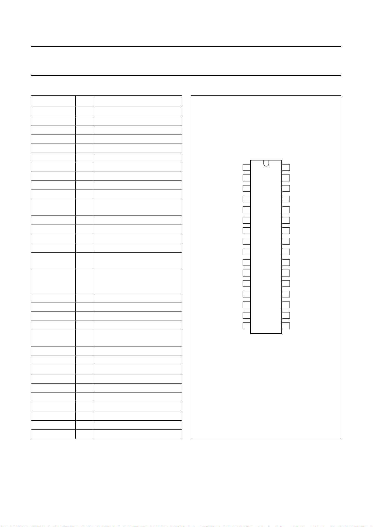
PINNING
SYMBOL PIN DESCRIPTION
−(R−Y) 1 output signal for −(R−Y)
−(B−Y) 2 output signal for −(B−Y)
U
in
V
in
SCL 5 serial clock input
SDA 6 serial data input/output
V
CC
DEC 8 digital supply decoupling
DGND 9 digital ground
SC 10 sandcastle output
VA 11 vertical acquisition
Y
out
V
out
U
out
I/O PORT 15 input/output port
O PORT/LLC 16 output port/line-locked clock
CLP/HA 17 clamping pulse/HA
F 18 fast switch select input
B 19 BLUE input
G 20 GREEN input
R 21 RED input
ADDR (CVBS) 22 I
Fscomb 23 comb filter status input/output
HPLL 24 horizontal PLL filter
C 25 chrominance input
Y/CVBS 26 luminance/CVBS input
AGND 27 analog ground
FILT
ref
CPLL 29 colour PLL filter
XTAL 30 reference crystal input
XTAL2 31 second crystal input
SEC
ref
3 chrominance U input
4 chrominance V input
7 positive supply voltage
synchronization pulse
12 luminance output
13 chrominance V output
14 chrominance U output
output
synchronization pulse
input/output
2
C-bus address input (CVBS
output)
28 filter reference decoupling
32 SECAM reference decoupling
handbook, halfpage
−(R−Y)
−(B−Y)
U
V
SCL
SDA
V
CC
DEC
DGND
SC
VA
Y
out
V
out
U
out
I/O PORT
O PORT/LLC
Fig.2 Pin configuration.
TDA9143
1
2
3
in
4
in
5
6
7
8
TDA9143
9
10
11
12
13
14
15
16
MGE038
SEC
32
XTAL2
31
XTAL
30
CPLL
29
FILT
28
AGND
27
Y/CVBS
26
C
25
HPLL
24
Fscomb
23
ADDR (CVBS)
22
R
21
G
20
B
19
F
18
CLP/HA
17
ref
ref
1996 Jan 17 5

Philips Semiconductors Preliminary specification
I2C-bus controlled, alignment-free
PAL/NTSC/SECAM decoder/sync processor
FUNCTIONAL DESCRIPTION
The TDA9143 is an I2C-bus controlled, alignment-free
PAL/NTSC/SECAM colour decoder/sync processor which
has been designed for use with baseband chrominance
delay lines. For PALplus and EDTV-2 (60 Hz) signals
blanking facilities are included.
In the standard operating mode the I2C-bus address is 8A.
If the address input is connected to the positive supply rail
the address will change to 8E.
Input switch
CAUTION
The voltage on the chrominance pin must never exceed
5.5 V. If it does, the IC enters a test mode.
The TDA9143 has a two pin input for CVBS or Y/C signals
which can be selected via the I
also has a position in which it automatically detects
whether a CVBS or Y/C signal is on the input. In this input
selector position, standard identification first takes place
on an added Y/CVBS and C input signal.
After that, both chrominance signal input amplitudes are
checked once and the input with the strongest
chrominance burst signal is selected. The input switch
status is read out by the I2C-bus via output bit YC. The
auto input detector indicates YC = 1 for a VBS input signal
(no chrominance component).
CVBS output
In the standard operating mode with I
a CVBS output signal is available on the address pin,
which represents either the CVBS input signal or the Y/C
input signal, added into a CVBS signal.
RGB colour matrix
The voltage on the Uin pin must never exceed 5.5 V.
If it does, the IC enters a test mode.
The TDA9143 has a colour matrix to convert RGB input
signals into YUV signals. A fast switch, controlled by the
signal on pin F and enabled by I
fast switch), can select between these YUV signals and
the YUV signals of the decoder. Mode FRGB = 1 (forced
RGB) overrules EFS and switches the matrixed RGB
inputs to the YUV outputs.
2
C-bus. The input selector
CAUTION
2
2
C-bus address 8A,
C-bus via EFS (enable
The Y signal is internally connected to the switch. The
−(R−Y) and−(B−Y) output signals of the decoder first have
to be delayed in external baseband chrominance delay
lines. The outputs of the delay lines must be connected to
the UV input pins. If the RGB signals are not synchronous
with the selected decoder input signal, clamping of the
RGB input signals is possible by I2C-bus selection of ECL
(external RGB clamp mode) and by feeding an external
clamping signal to the CLP pin.
Also in external RGB clamp mode the VA output will be in
a high impedance OFF-state. The YUV outputs can be put
in 3-state mode by bus bit LPS (low power standby mode).
Standard identification
The standards which the TDA9143 can decode depend
upon the choice of external crystals. If a 4.4 MHz and a
3.6 MHz crystal are used then SECAM, PAL 4.4/3.6 and
NTSC 4.4/3.6 can be decoded. If two 3.6 MHz crystals are
used then only PAL 3.6 and NTSC 3.6 can be decoded.
Which 3.6 MHz standards can be decoded depends upon
the exact frequencies of the 3.6 MHz crystals. In an
application where not all standards are required only one
crystal is sufficient; in this instance the crystal must be
connected to the reference crystal input (pin 30). If a
4.4 MHz crystal is used it must always be connected to the
reference crystal input. Both crystals are used to provide a
reference for the filters and the horizontal PLL, however,
only the reference crystal is used to provide a reference for
the SECAM demodulator. To enable the calibrating circuits
to be adjusted exactly, two bits from I
00 are used to indicate which crystals are connected to the
IC.
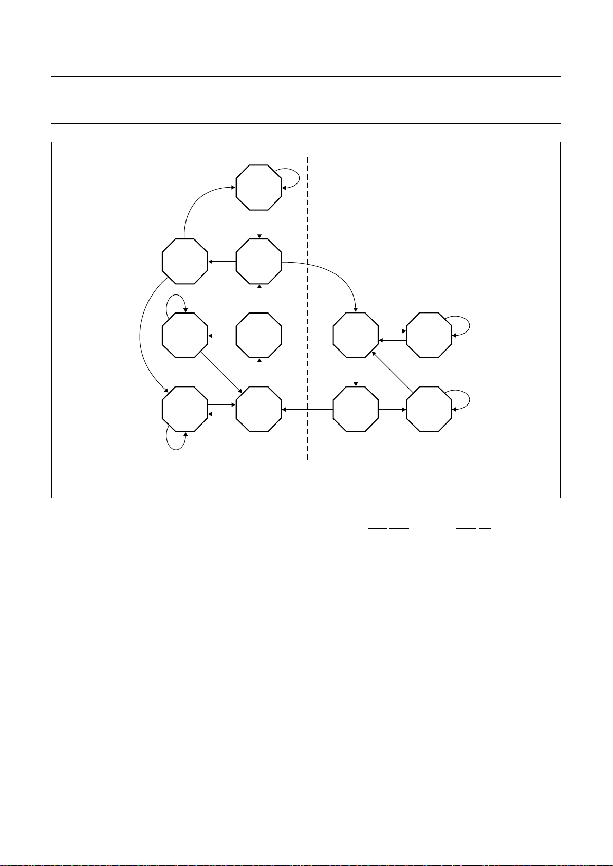
The standard identification circuit is a digital circuit without
external components. The search loop is illustrated
in Fig.3. The decoder (via the I2C-bus) can be forced to
decode either SECAM or PAL/NTSC (but not PAL or
NTSC). Crystal selection can also be forced. Information
concerning standard and which crystal is selected and
whether the colour killer is ON or OFF is provided by the
read out.
Using the forced-mode does not affect the search loop, it
does however prevent the decoder from reaching or
staying in an unwanted state. The identification circuit
skips impossible standards (e.g. SECAM when no
4.4 MHz crystal is fitted) and illegal standards (e.g. in
forced mode). To reduce the risk of wrong identification,
PAL has priority over SECAM. Only line identification is
used for SECAM. For a vertical frequency of 60 Hz,
SECAM can be blocked to prevent wrong identification by
means of bus bit SAF.
TDA9143
2
C-bus subaddress
1996 Jan 17 6
Philips Semiconductors Preliminary specification
I2C-bus controlled, alignment-free
PAL/NTSC/SECAM decoder/sync processor
handbook, full pagewidth
SECAM
c
c
PAL
KILLED
NTSC
SECAM
KILLED
NTSC
c
c
KILLED
PAL
KILLED
c
c
c
TDA9143
PAL
KILLED
c
c
NTSC
KILLED
PAL
c
c
NTSCPAL
Reference crystal Second crystal
Fig.3 Search loop of the identification circuit.
Integrated filters
All chrominance bandpass and notch filters, including the
luminance delay line, are an integral part of the IC. The
filters are gyrator-capacitor type filters. The resonant
frequency of the filters is controlled by a circuit that uses
the active crystal to tune the SECAM Cloche filter during
the vertical flyback time. The remaining filters and the
luminance delay line are matched to this filter. The filters
can be switched to either 4.43 MHz, 4.29 MHz or
3.58 MHz. The switching is controlled by the standard
identification circuit. The luminance notch used for
SECAM has a lower Q-factor than the notch used for
PAL/NTSC. The notches are provided with a little preshoot
to obtain a symmetrical step response. In Y/C mode the
chrominance notch filters are bypassed, to preserve full
signal bandwidth. For a CVBS signal the chrominance
notch filters can be bypassed by bus selection of bit TB
(trap bypass). The delay of the colour difference signals
−(R−Y) and−(B−Y) in the chrominance signal path and the
external chrominance delay lines when used, can be fitted
2
to the luminance signal by I
C-bus in 40 ns steps.
MGE040
The typical luminance delay can be calculated:
delay ≈ 90 +
SAK⋅SBK {170 + 40(FRQ⋅TB)} + 160(YD3) +
160(YD2) + 80(YD1) + 40(YD0) [ns].
Colour decoder
The PAL/NTSC demodulator employs an oscillator that
can operate with either crystal (3.6 MHz or 4.4 MHz). If the
2
C-bus indicates that only one crystal is connected, it will
I
always connect to the crystal on the reference crystal input
(pin 30).
The Hue signal which is adjustable by I2C-bus, is gated
during the burst for NTSC signals.
The SECAM demodulator is an auto-calibrating PLL
demodulator which has two references. The reference
crystal, to force the PLL to the desired free-running
frequency and the bandgap reference, to obtain the
correct absolute value of the output signal. The VCO of the
PLL is calibrated during each vertical blanking period,
when the IC is in search mode or in SECAM mode.
1996 Jan 17 7
Philips Semiconductors Preliminary specification
I2C-bus controlled, alignment-free
PAL/NTSC/SECAM decoder/sync processor
If the reference crystal is not 4.4 MHz the decoder will not
produce the correct SECAM signals. Especially for NTSC
applications an internal bypass mode of the external
baseband delay line (for instance TDA4665) is added,
controlled by bus bit BPS (bypass mode) and with a gain
of 2. The bypass mode is not available for SECAM.
Comb filter interfacing
The frequency of the active crystal is fed to the Fscomb
output, which can be connected to an external comb filter
IC (e.g. SAA4961). When bus bit ECMB is LOW, the
subcarrier frequency is suppressed and its DC value is
LOW. With ECMB HIGH, the DC value is HIGH with the
2
subcarrier frequency present, and I
C-bus output bit YC
and the input switch are always forced in the Y/C mode,
unless an external current sink (e.g. from the comb filter)
prevents this, as pin Fscomb also acts as input pin. In this
event the subcarrier frequency is still present on the same
DC HIGH level.
PALplus and EDTV-2 helper blanking
For blanking of PALplus or EDTV-2 helper lines, the helper
blanking can extend the vertical blanking of the Y, R−Y and
B−Y outputs. Additional helper blanking bits (HOB, HBC)
and norm/not norm (NRM) indication determine whether
the helper signal has to be blanked or conditionally
blanked depending on the signal-to-noise ratio bit SNR.
Table 1 is valid in a 50 Hz or 60 Hz mode.
Provided a NORM sync condition is present, with bus bit
HBO = 1 and HBC = 0 blanking is activated. Conditional
blanking is possible with HBO = 1 and HBC = 1 and
SNR = 1.
The black level of the luminance signal is internally
clamped with a large time constant to an internal reference
black level. This black level is used as fill-in value for the Y
signal during blanking.
Fast blanking detector
To detect the presence of a fast blanking signal, a circuit is
added which indicates this event if in more than one line
per field a blanking pulse is present at the fast blanking
input (F). More than one line per field is chosen to prevent
switching-off at every spike detected on the fast blanking
input. The detector output FBA (fast blanking active) can
be read-out by the I
Blanked/unblanked sync
By means of the I
signal Y
sync part. At BSY = 0 the composite sync is present on
Y
during helper lines scan. At BSY = 1 the black level is filled
in during the line blanking interval and vertical blanking
interval. When activated, the helper blanking extends the
vertical blanking.
TDA9143
2
C-bus.
2
C-bus bit BSY (blanked sync) output
will be presented with or without its composite
out
. When activated, helper blanking takes place only
out
Table 1 Helper blanking modes
HOB HBC SNR
HELPER
BLANKING
0 X X OFF
10XON
110OFF
111 ON
For PALplus (50 Hz, 625 lines) outside the letter box area
blanking is possible and takes place on lines 275 to 371
and 587 to 59.
For EDTV-2 (system M, 60 Hz, 525 lines) outside the letter
box area blanking is possible and takes place on lines 230
(1)
to 312 and 493 to 49
(1) For system M, line numbers start with the first equalizing
pulse in field 1, but the internal line counter starts counting at
the first vertical sync pulse in field 1. This line number
notation is used here and in Fig.7.
.
1996 Jan 17 8
Sync processor (ϕ
loop)
1
The main part of the sync circuit is an oscillator running at
440 × f
(6.875 MHz), provided that I2C-bus address 8A is
H
used or 432 × fH (6.75 MHz) for 8E. Its frequency is divided
by 440 or 432 to lock the ϕ1 loop to the incoming signal.
The time-constant of the loop can be selected by the
2
C-bus (fast, auto or slow). In the fast mode the fast
I
time-constant is chosen independent of signal conditions.
In the auto mode the medium time-constant is present with
a fast time constant during the vertical retrace period (‘field
boost’). If the noise detector indicates a noisy video signal
the time-constant switches to slow with a smaller field
boost, which is also the time-constant for the slow mode.
In case of a slow time constant sync gating takes place in
a 6 µs window around the separated sync pulse. In case of
no sync lock, both the auto and the slow mode have a
medium time constant, to ensure reliable catching.
The noise content of the video signal is determined by a
noise detector circuit. This circuit measures the noise at
top sync during a 15 line period every field (65 lines after
start VA pulse). When the noise level supersedes the
Philips Semiconductors Preliminary specification
I2C-bus controlled, alignment-free
PAL/NTSC/SECAM decoder/sync processor
detector threshold in two consecutive fields, noise is
indicated and bus bit SNR is set.
The free-running frequency of the oscillator is determined
by a digital control circuit that is locked to the active crystal.
When a power-on-reset pulse is detected the frequency of
the oscillator is switched to a frequency of about 10 MHz
(23 kHz horizontal frequency) to protect the horizontal
output transistor. The oscillator frequency is calibrated to
6.875 MHz or 6.75 MHz after receiving data on
subaddress 01 for the first time after power-on-reset
detection.
To ensure that this procedure does not fail it is absolutely
necessary to send subaddress 00 before subaddress 01.
Subaddress 00 contains the crystal indication bits and
when subaddress 01 is received the line oscillator
calibration will be initiated (for the start-up procedure after
power-on-reset detection, see the I2C-bus protocol). The
calibration is terminated when the oscillator frequency
reaches 6.875 MHz or 6.75 MHz.
The ϕ1 loop can be opened using the I2C-bus. This is to
facilitate On Screen Display (OSD) information. If there is
no input signal or a very noisy input signal, the ϕ1 loop can
be opened to provide a stable line frequency, and thus a
stable picture.
The sync part also delivers a two-level sandcastle signal,
which provides a combined horizontal and vertical
blanking signal and a clamping pulse for the display
section of the TV.
MACROVISION sync gating
A dedicated gating signal for the separated sync pulses,
starting 11 lines after the detection of a vertical sync pulse
until picture scan starts, can be used to improve the
behaviour of the horizontal PLL with respect to the
unwanted disturbances caused by the pseudo-sync pulses
in video signals with MACROVISION anti-copy guard
signals. This sync gating excludes the pseudo-sync pulses
and can only take place in the auto and fast ϕ
constant mode, provided I2C-bus bit SNR = 0 and I2C-bus
bit EMG = 1. I2C-bus bit EMG = 1 enables and EMG = 0
disables this sync gating in the horizontal PLL.
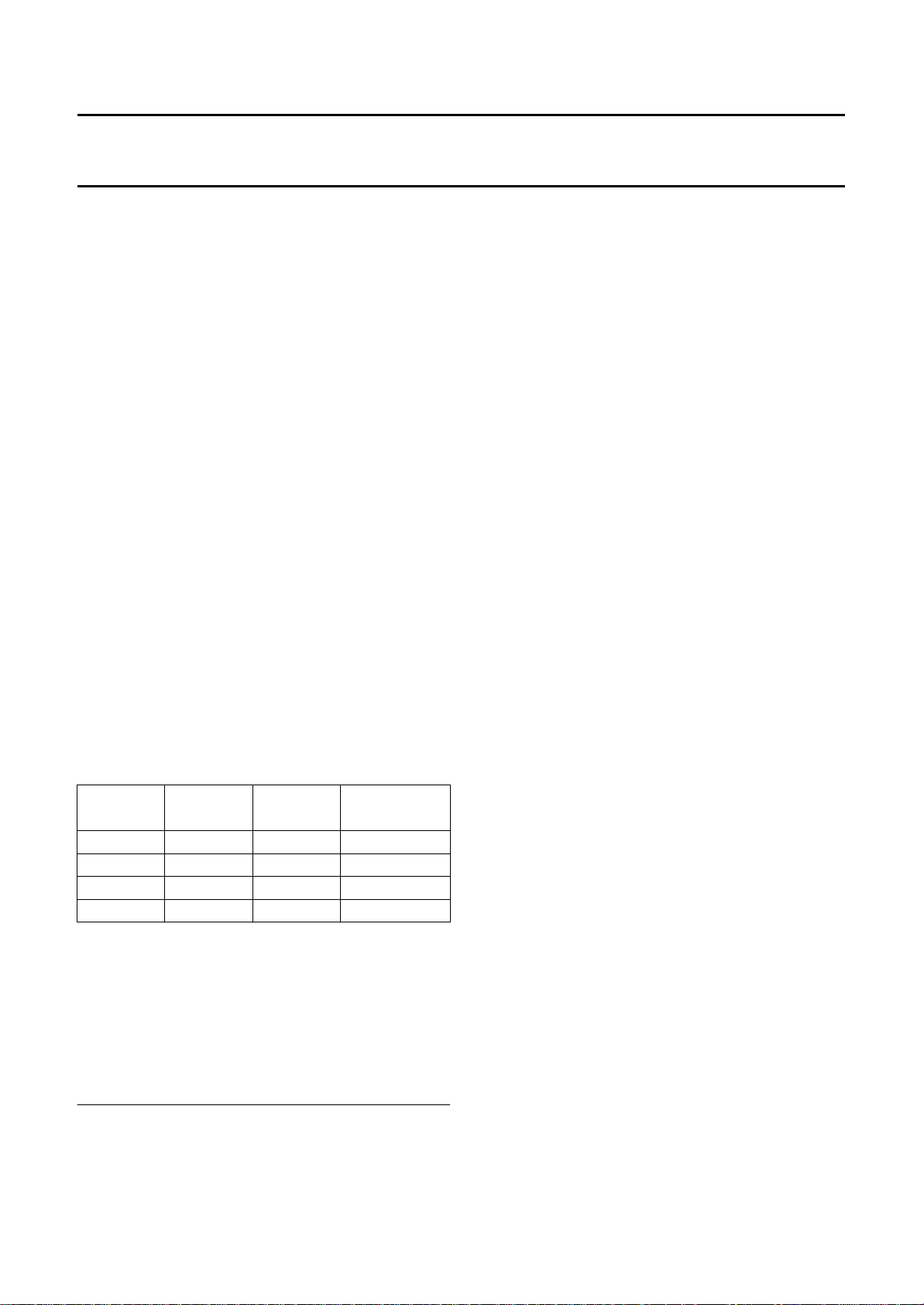
Vertical divider system
The vertical divider system has a fully integrated vertical
sync separator.
The divider can accommodate both 50 Hz and 60 Hz
systems; it can either determine the field frequency
automatically or it can be forced to the desired system via
the I
is illustrated in Fig.4.
TDA9143
time
1
2
C-bus. A block diagram of the vertical divider system
handbook, halfpage
LINE COUNTER
CONTROLLER
NORM COUNTER
Fig.4 Block diagram of the vertical divider system.
1996 Jan 17 9
TIMING
GENERATOR
MGE043
Philips Semiconductors Preliminary specification
I2C-bus controlled, alignment-free
PAL/NTSC/SECAM decoder/sync processor
The divider system operates at twice the horizontal
frequency. The line counter receives enable pulses at this
frequency, thereby counting two pulses per line. A state
diagram of the controller is shown in Fig.5. Because it is
symmetrical only the right-hand part will be described.
Depending on the previously found vertical frequency, the
controller will be in one of the COUNT states. When the
line counter has counted 488 pulses (i.e. 244 lines of the
video input signal), the controller will move to the next state
depending on the output of the norm counter. This can be
either NORM, NEAR_NORM or NO_NORM, depending
handbook, full pagewidth
no_norm
on the position of the vertical sync pulse in the previous
fields. When the controller is in the NORM state it
generates the vertical sync pulse (VSP) automatically and
then, when the line counter is at LC = 626, moves to the
WAIT state. In this condition it waits for the next pulse of
the double line frequency signal, and then moves to the
COUNT state of the current field frequency. When the
controller returns to the COUNT state, the line counter will
be reset half a line after the start of the vertical sync pulse
of the video input signal. The NORM window normally
looks within one line width and a sudden half line delay of
the vertical sync pulse change can therefore be neglected.
else
NO
NORM
TDA9143
no_norm
LC = 528 or LC = 576 or on VSP LC = 628 or LC = 722 or on VSP
LC < 488
norm norm
near_norm near_norm
on VSP if
522 < LC < 528
or on LC = 528
vertical frequency 60 Hz vertical frequency 50 Hz
on SYNC
if LC < 576
LC = 526 LC = 626
NORM
LC ≤ 525 LC ≤ 625
NEAR
NORM
LC < 522 LC < 622
WAIT
FOR
RESET
PULSE
on SYNC
if LC ≥ 576
NORM
NEAR
NORM
COUNTCOUNT
LC < 488
on VSP if
622 < LC < 628
or on LC = 628
MGE042
1996 Jan 17 10
Fig.5 State diagram of the vertical divider system.
Philips Semiconductors Preliminary specification
I2C-bus controlled, alignment-free
PAL/NTSC/SECAM decoder/sync processor
When the controller is in the NEAR_NORM state it will
move to the COUNT state if it detects the vertical sync
pulse within the NEAR_NORM window (i.e.
622 < LC < 628). If no vertical sync pulse is detected the
controller will move back to the COUNT state when the line
counter reaches LC = 628. The line counter will then be
reset.
When the controller is in the NO_NORM state, it will move
to the COUNT state when it detects a vertical sync pulse
and reset the line counter. If a vertical sync pulse is not
detected before LC = 722 (if the ϕ1 loop is locked in forced
mode) it will move to the COUNT state and reset the line
counter. If theϕ1 loop is not locked the controller will return
to the COUNT state when LC = 628.
The forced mode option keeps the controller in either the
left-hand side (60 Hz) or the right-hand side (50 Hz) of the
state diagram.
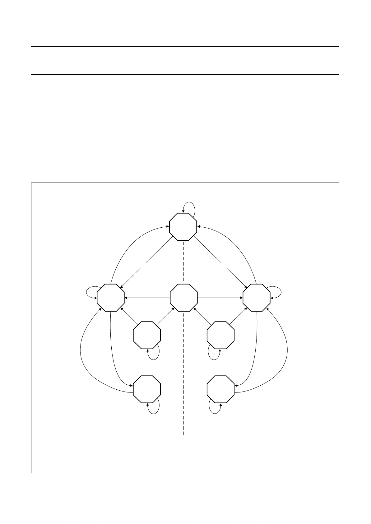
Figure 6 illustrates the state diagram of the norm counter
which is an up/down counter that increases its counter
value by 1 if it finds a vertical sync pulse within the selected
window. If not, it decreases the counter value by 1 (or 2,
see Fig.6). In the NEAR_NORM and NORM states the first
correct vertical sync pulse after one or more incorrect
vertical sync pulses is processed as an incorrect pulse.
This procedure prevents the system from staying in the
NEAR_NORM or NORM state if the vertical sync pulse is
correct in the first field and incorrect in the second field.
In case of no sync lock (SLN = 1) the norm counter is reset
to NO_NORM (wide search window), for fast vertical
catching when switching between video sources. Fast
switching between different channels however can still
result in a continuous horizontal sync lock situation, when
the channel is changed before the norm counter has
reached the NORM state. To provide faster vertical
catching in this case, measures have been taken to
prevent the norm counter to count down to zero before
reaching the NO_NORM state (see left-hand of Fig.6). Bus
bit FWW (forced wide window) enables the norm counter
to stay in the NO_NORM state if desired. The
norm/no_norm status is read out by bus bit NRM.
TDA9143
handbook, full pagewidth
10 < NC < 26
(1) VSP found: count 1 up; no VSP found: count 2 down.
22 < NC ≤ 27 0 ≤ NC < 12
NC = 26
(1)
NC = 17
10 < NC < 17
NORM
NEAR
NORM
NEAR
NORM
norm test area near_norm test area
NC = 22
(RESET NC)
NC = 10
(RESET NC)
NC = 10
(RESET NC)
NC = 14
NC = 0
NO
NORM
NC = 12
NEAR
NORM
0 < NC < 14
MGE041
1996 Jan 17 11
Fig.6 State diagram of the norm counter.
 Loading...