


DATA SH EET
Product specification
File under Integrated Circuits, IC02
December 1992
INTEGRATED CIRCUITS
TDA9141
PAL/NTSC/SECAM decoder/sync
processor

December 1992 2
Philips Semiconductors Product specification
PAL/NTSC/SECAM decoder/sync processor TDA9141
FEATURES
• Multistandard PAL, NTSC and SECAM
• I2C-bus controlled
• I2C-bus addresses can be selected by hardware
• Alignment free
• Few external components
• Designed for use with baseband delay lines
• Integrated video filters
• CVBS or YC input with automatic detection
• CVBS output
• Vertical divider system
• Two-level sandcastle signal
• VA synchronization pulse (3-state)
• HA synchronization pulse or clamping pulse CLP
input/output
• Line-locked clock output or stand-alone I2C-bus output
port
• Stand-alone I2C-bus input/output port
• Colour matrix and fast YUV switch
• Comb filter enable input/output with subcarrier
frequency.
GENERAL DESCRIPTION
The TDA9141 is an I2C-bus controlled, alignment-free
PAL/NTSC/SECAM decoder/sync processor. The
TDA9141 has been designed for use with baseband
chrominance delay lines, and has a combined subcarrier
frequency/comb filter enable signal for communication
with a PAL comb filter.
The IC can process CVBS signals and Y/C input signals.
The input signal is available on an output pin, in the event
of a Y/C signal, it is added into a CVBS signal.
The sync processor provides a two-level sandcastle, a
horizontal pulse (CLP or HA pulse, bus selectable) and a
vertical (VA) pulse. When the HA pulse is selected a
line-locked clock (LLC) signal is available at the output port
pin.
A fast switch can select either the internal Y signal with the
UV input signals, or YUV signals made of the RGB input
signals. The RGB input signals can be clamped with either
the internal or an external clamping signal (search tuning
mode).
Two pins with an input/output port and an output port of the
I2C-bus are available.
The I2C-bus address of the TDA9141 is hardware
programmable.
ORDERING INFORMATION
Note
1. SOT232-1; 1996 December 4.
EXTENDED TYPE
NUMBER
PACKAGE
PINS PIN POSITION MATERIAL CODE
TDA9141 32 SDIL plastic SOT232
(1)
December 1992 3
Philips Semiconductors Product specification
PAL/NTSC/SECAM decoder/sync
processor
TDA9141
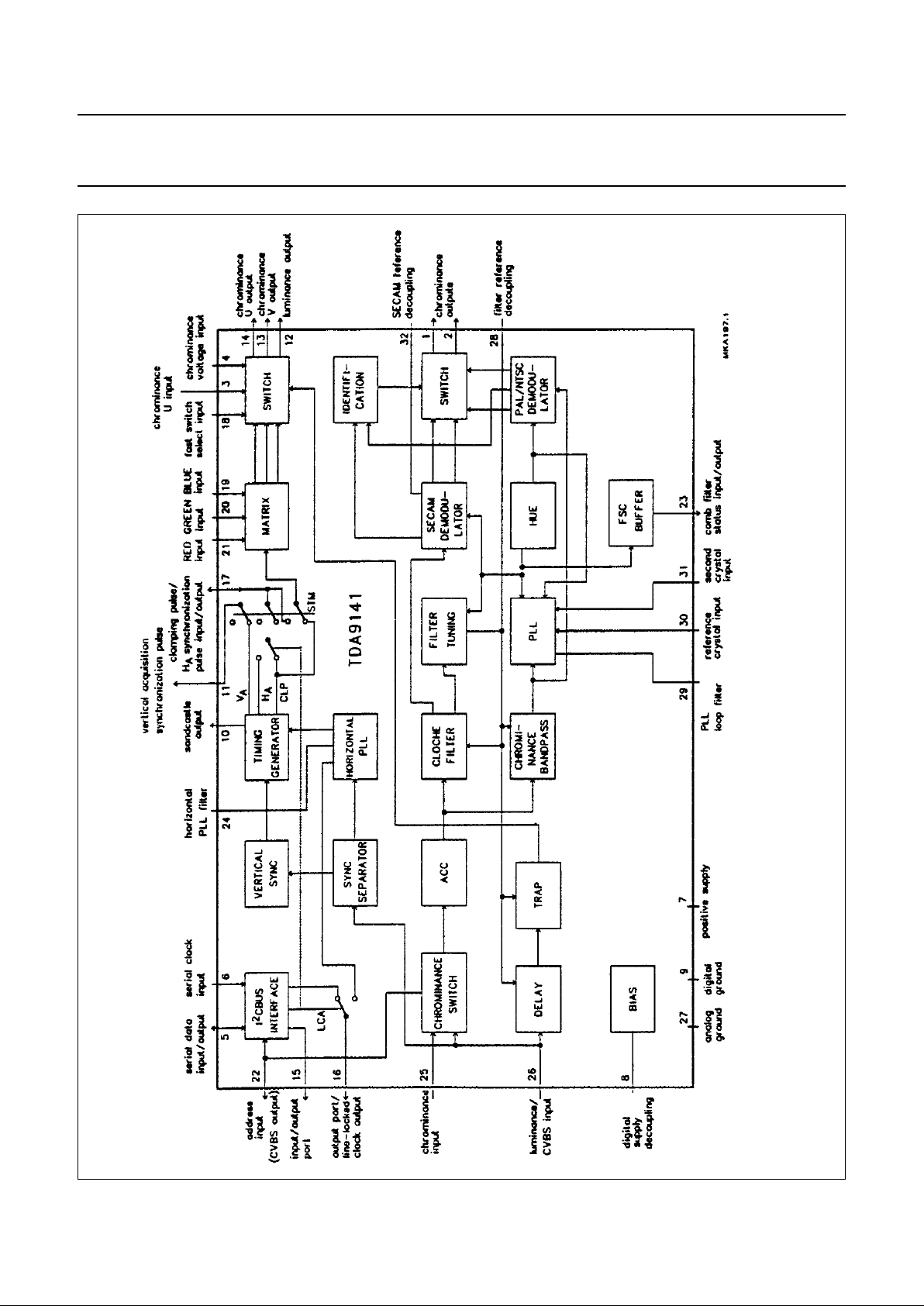
Fig.1 Block diagram.
December 1992 4
Philips Semiconductors Product specification
PAL/NTSC/SECAM decoder/sync processor TDA9141
QUICK REFERENCE DATA
SYMBOL PARAMETER CONDITIONS MIN. TYP. MAX. UNIT
V
CC
positive supply voltage 7.2 8.0 8.8 V
I
CC
supply current − 45 − mA
V
26(p-p)
CVBS input voltage (peak-to-peak value) top sync - white − 1.0 − V
V
26(p-p)
luminance input voltage (peak-to-peak value) top sync - white − 1.0 − V
V
22(p-p)
chrominance burst input voltage (peak-to-peak
value)
− 0.3 − V
V
12
luminance black-white output voltage − 1.0 − V
V
14(p-p)
U output voltage (peak-to-peak value) standard colour bar − 1.33 − V
V
13(p-p)
V output voltage (peak-to-peak value) standard colour bar − 1.05 − V
V
10
sandcastle blanking voltage level − 2.5 − V
V
10
sandcastle clamping voltage level − 4.5 − V
V
11
VA output voltage − 5.0 − V
V
17
HA output voltage − 5.0 − V
V
16(p-p)
LLC output voltage amplitude (peak-to-peak value) − 500 − mV
V
21,20 19(p-p)
RGB input voltage (peak-to-peak value) 0 to 100%
saturation
− 0.7 − V
V
clamp I/O
clamping pulse input/output voltage − 5.0 − V
V
sub
subcarrier output voltage amplitude
(peak-to-peak value)
− 200 − mV
V
15,16
O port output voltage − 5.0 − V
December 1992 5
Philips Semiconductors Product specification
PAL/NTSC/SECAM decoder/sync processor TDA9141
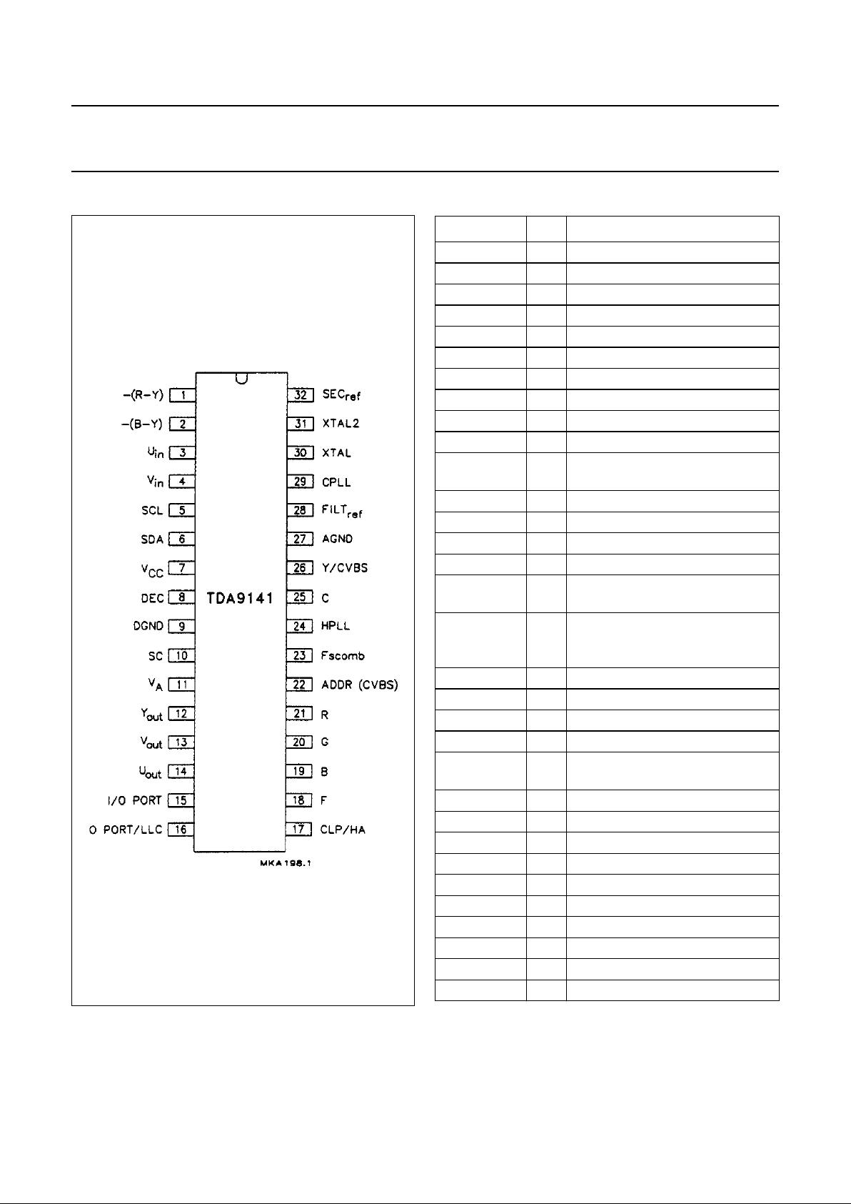
Fig.2 Pin configuration.
PINNING
SYMBOL PIN DESCRIPTION
−(R−Y) 1 chrominance output
−(B−Y) 2 chrominance output
U
in
3 chrominance U input
V
in
4 chrominance voltage input
SCL 5 serial clock input
SDA 6 serial data input/output
V
CC
7 positive supply input
DEC 8 digital supply decoupling
DGND 9 digital ground
SC 10 sandcastle output
V
A
11 vertical acquisition
synchronization pulse
Y
out
12 luminance output
V
out
13 chrominance V output
U
out
14 chrominance U output
I/O PORT 15 input/output port
O PORT/LLC 16 output port/line-locked clock
output
CLP/HA 17 clamping pulse/H
A
synchronization pulse
input/output
F 18 fast switch select input
B 19 BLUE input
G 20 GREEN input
R 21 RED input
ADDR
(CVBS)
22 I
2
C-bus address input (CVBS
output)
Fscomb 23 comb filter status input/output
HPLL 24 horizontal PLL filter
C 25 chrominance input
Y/CVBS 26 luminance/CVBS input
AGND 27 analog ground
FILT
ref
28 filter reference decoupling
CPLL 29 colour PLL filter
XTAL 30 reference crystal input
XTAL2 31 second crystal input
SEC
ref
32 SECAM reference decoupling

December 1992 6
Philips Semiconductors Product specification
PAL/NTSC/SECAM decoder/sync
processor
TDA9141
FUNCTIONAL DESCRIPTION
General
The TDA9141 is an I
2
C-bus
controlled, alignment-free
PAL/NTSC/SECAM colour
decoder/sync processor which has
been designed for use with baseband
chrominance delay lines.
In the standard operating mode the
I2C-bus address is 8A. If the address
input is connected to the positive rail
the address will change to 8E.
Input switch
WARNING: T
HE VOLTAGE ON THE
CHROMINANCE PIN MUST NEVER
EXCEED
5.5 V. IF IT DOES THE IC
ENTERS A TEST MODE.
The TDA9141 has a two pin input for
CVBS or YC signals which can be
selected via the I2C-bus. The input
selector also has a position in which it
automatically detects whether a
CVBS or YC signal is on the input. In
this input selector position, standard
identification first takes place on an
added Y/CVBS and C input signal.
After that, both chrominance signal
input amplitudes are checked once
and the input with the strongest
chrominance burst signal is selected.
The input switch status is read out by
the I2C-bus via output bit YC.
CVBS output
In the standard operating mode with
the I
2
C-bus address 8A, a CVBS
output signal is available on the
address pin, which represents either
the CVBS input signal or the Y/C input
signal, added into a CVBS signal
RGB colour matrix
WARNING: THE VOLTAGE ON THE UIN
PIN MUST NEVER EXCEED
5.5 V. IFIT
DOES THE
IC ENTERS A TEST MODE.
The TDA9141 has a colour matrix to
convert RGB input signals into YUV
signals. A fast switch, controlled by
the signal on pin F and enabled by the
I
2
C-bus via EFS (enable fast switch),
can select between these YUV
signals and the YUV signals of the
decoder. The Y signal is internally
connected to the switch. The −(R−Y)
and −(B−Y) output signals of the
decoder have to first be delayed in
external baseband chrominance
delay lines. The outputs of the delay
lines must be connected to the UV
input pins. If the RGB signals are not
synchronous with the selected
decoder input signal, clamping of the
RGB input signals is possible by
I
2
C-bus selection of STM (search
tuning mode), EFS and by feeding an
external clamping signal to the CLP
pin.
Also in search tuning mode the VA
output will be in a high impedance
OFF-state.
Standard identification
The standards which the TDA9141
can decode are dependent on the
choice of external crystals. If a
4.4 MHz and a 3.6 MHz crystal are
used then SECAM, PAL 4.4/3.6 and
NTSC 4.4/3.6 can be decoded. If two
3.6 MHz crystals are used then only
PAL 3.6 and NTSC 3.6 can be
decoded. Which 3.6 MHz standards
can be decoded is dependent on the
exact frequencies of the 3.6 MHz
crystals. In an application where not
all standards are required only one
crystal is sufficient (in this instance
the crystal must be connected to the
reference crystal input (pin 30)). If a
4.4 MHz crystal is used it must always
be connected to pin 30. Both crystals
are used to provide a reference for
the filters and the horizontal PLL,
however, only the reference crystal is
used to provide a reference for the
SECAM demodulator.
To enable the calibrating circuits to be
adjusted exactly two bits from I
2
C-bus
subaddress 00 are used to indicate
which crystals are connected to the
IC.
The standard identification circuit is a
digital circuit without external
components; the search loop is
illustrated in Fig.3.
The decoder (via the I
2
C-bus) can be
forced to decode either SECAM or
PAL/NTSC (but not PAL or NTSC).
Crystal selection can also be forced.
Information concerning which
standard and which crystal have been
selected and whether the colour killer
is ON or OFF is provided by the read
out. Using the forced-mode does not
affect the search loop, it does,
however, prevent the decoder from
reaching or staying in an unwanted
state. The identification circuit skips
impossible standards (e.g. SECAM
when no 4.4 MHz crystal is fitted) and
illegal standards (e.g. is forced
mode). To reduce the risk of wrong
identification PAL has priority over
SECAM (only line identification is
used for SECAM).
Integrated filters
All filters, including the luminance
delay line, are an integral part of the
IC. The filters are gyrator-capacitor
type filters. The resonant frequency of
the filters is controlled by a circuit that
uses the active crystal to tune the
SECAM Cloche filter during the
vertical flyback time. The remaining
filters and the luminance delay line
are matched to this filter. The filters
can be switched to either 4.43 MHz,
4.28 MHz or 3.58 MHz irrespective of
the frequency of the active crystal.
The switching is controlled by the
identification circuit.
In YC mode the chrominance notch
filter is bypassed, to preserve full
signal bandwidth.
For a CVBS signal the chrominance
notch filter can be bypassed by
I
2
C-bus selection of TB (trap bypass).
The luminance delay line delivers the
Y signal to the output 60 ns after the
−(R−Y) and −(B−Y) signals have
arrived at their outputs.

December 1992 7
Philips Semiconductors Product specification
PAL/NTSC/SECAM decoder/sync
processor
TDA9141
This compensates for the delay of the
external chrominance delay lines.
Colour decoder
The PAL/NTSC demodulator
employs an oscillator that can operate
with either crystal (3.6 or 4.4 MHz). If
the I
2
C-bus indicates that only one
crystal is connected it will always
connect to the crystal on the
reference crystal input (pin 30).
The Hue signal, which is adjustable
via the I2C-bus, is gated during the
burst for NTSC signals.
The SECAM demodulator is an
auto-calibrating PLL demodulator
which has two references. The
reference crystal, to force the PLL to
the desired free-running frequency
and the bandgap reference, to obtain
the correct absolute value of the
output signal. The VCO of the PLL is
calibrated during each vertical
blanking period, when the IC is in
search mode or SECAM mode. If the
reference crystal is not 4.4 MHz the
decoder will not produce the correct
SECAM signals.
The frequency of the active crystal is
fed to the Fscomb output, which can
be connected to an external comb
filter IC. The DC value on this pin
contains the comb enable
information. Comb enable is true
when bus bit ECMB is HIGH. If ECMB
is LOW, the subcarrier frequency is
suppressed. The external comb filter
can force the DC value of Fscomb
LOW, as pin Fscomb also acts as
input pin. In this event the subcarrier
frequency is still present. If the DC
value of Fscomb is HIGH, the input
switch is always forced in Y/C mode,
indicated by bus bit YC.
Sync processor (ϕ1 loop)
The main part of the sync circuit is a
432 × fH (6.75 MHz) oscillator the
frequency of which is divided by 432
to lock the Phase 1 loop to the
incoming signal. The time constant of
the loop can be forced by the I2C-bus
(fast or slow). If required the IC can
select the time constant, depending
on the noise content of the input
signal and whether the loop is
phase-locked or not (medium or
slow). The free-running frequency of
the oscillator is determined by a
digital control circuit that is locked to
the active crystal.
When a power-on-reset pulse is
detected the frequency of the
oscillator is switched to a frequency
greater than 6.75 MHz to protect the
horizontal output transistor. The
oscillator frequency is reset to
6.75 MHz when the crystal indication
bits have been loaded into the IC. To
ensure that this procedure does not
fail it is absolutely necessary to send
subaddress 00 before subaddress
01. Subaddress 00 contains the
crystal indication bits and when
subaddress 01 is received the line
oscillator calibration will be initiated
(for the start-up procedure after
power-on reset detection see the
I2C-bus protocol. The calibration is
terminated when the oscillator
frequency reaches 6.75 MHz. The
oscillator is again calibrated when an
out-of-lock condition with the input
signal is detected by the coincidence
detector. Again the calibration will be
terminated when the oscillator
frequency reaches 6.75 MHz.
The Phase 1 loop can be opened
using the I2C-bus. This is to facilitate
On Screen Display (OSD)
information. If there is no input signal
or a very noisy input signal the phase
1 loop can be opened to provide a
stable line frequency and thus a
stable picture.
The sync part also delivers a
two-level sandcastle signal, which
provides a combined horizontal and
vertical blanking signal and a
clamping pulse for the display section
of the TV.
Vertical divider system
The vertical divider system has a fully
integrated vertical sync separator.
The divider can accommodate both
50 and 60 Hz systems; it can either
locate the field frequency
automatically or it can be forced to the
desired system via the I2C-bus. A
block diagram of the vertical divider
system is illustrated in Fig.4. The
divider system operates at twice the
horizontal line frequency. The line
counter receives enable pulses at this
line frequency, thereby counting two
pulses per line.
A state diagram of the controller is
illustrated in Fig.5. Because it is
symmetrical only the right hand part
will be described.
Depending on the previously found
field frequency, the controller will be
in one of the COUNT states. When
the line counter has counted 488
pulses (i.e. 244 lines of the video
input signal) the controller will move
to the next state depending on the
output of the norm counter. This can
be either NORM, NEAR_NORM or
NO_NORM depending on the
position of the vertical sync pulse in
the previous fields. When the
controller is in the NORM state it
generates the vertical sync pulse
(VSP) automatically and then, when
the line counter is at LC = 626,
moves to the WAIT state. In this
condition it waits for the next pulse of
the double line frequency signal and
then moves to the COUNT state of
the current field frequency. When the
controller returns to the COUNT state
the line counter will be reset half a line
after the start of the vertical sync
pulse of the video input signal.

December 1992 8
Philips Semiconductors Product specification
PAL/NTSC/SECAM decoder/sync
processor
TDA9141
When the controller is in the
NEAR_NORM state it will move to the
COUNT state if it detects the vertical
sync pulse within the NEAR_NORM
window (i.e. 622 < LC < 628). If no
vertical sync pulse is detected, the
controller will move back to the
COUNT state when the line counter
reaches LC = 628. The line counter
will then be reset.
When the controller is in the
NO_NORM state it will move to the
COUNT state when it detects a
vertical sync pulse and reset the line
counter. If a vertical sync pulse is not
detected before LC = 722 (if the
Phase 1 loop is locked in forced
mode) it will move to the COUNT
state and reset the line counter. If the
Phase 1 loop is not locked the
controller will move back to the
COUNT state when LC = 628.
The forced mode option keeps the
controller in either the left-hand side
(60 Hz) or the right-hand side (50 Hz)
of the state diagram.
Figure 6 illustrates the state diagram
of the norm counter which is an
up/down counter that counts up if it
finds a vertical sync pulse within the
selected window. In the
NEAR_NORM and NORM states the
first correct vertical sync pulse after
one or more incorrect vertical sync
pulses is processed as an incorrect
pulse. This procedure prevents the
system from staying in the
NEAR_NORM or NORM state if the
vertical sync pulse is correct in the
first field and incorrect in the second
field. If no vertical sync pulse is found
in the selected window this will always
result in a down pulse for the norm
counter.
Output port and input/output port
Two stand-alone ports are available
for external use. These ports are
I
2
C-bus controlled, the output port by
bus bit OPB and the input/output port
by bus bit OPA. Bus bit OPA is an
open-drain output, to enable input
port functioning. The pin status is
read out by bus via output bit IP.
Sandcastle
Figure 7 illustrates the timing of the
acquisition sandcastle (ASC) and the
V
A
pulse with respect to the input
signal. The sandcastle signal is in
accordance with the 2-level 5 V
sandcastle format. An external
vertical guard current can overrule the
sink current to enable blanking
purposes.
 Loading...