

Philips TDA9112 Service Manual
TDA9112
LOW-COST I2C CONTROLLED DEFLECTION PROCESSOR
FOR MULTISYNC MONITOR
FEATURES
General
■ ADVANCED I
2
C BUS CONTROLLED
DEFLECTION PROCESSOR DEDICATED
FOR HIGH-END CRT MONITORS
■ SINGLE SUPPLY VOLTAGE 12V
■ VERY LOW JITTER
■ DC/DC CONVERTER CONTROLLER
■ ADVANCED EW DRIVE
■ ADVANCED ASYMMETRY CORRECTIONS
■ AUTOMATIC MULTISTANDARD
SYNCHRONIZATION
■ 2 DYNAMIC CORRECTION WAVEFORM
OUTPUTS
■ X-RAY PROTECTION AND SOFT-START &
STOP ON HORIZONTAL AND DC/DC DRIVE
OUTPUTS
2
■ I
C BUS STATUS REGISTER
Horizontal section
■ 150 kHz maximum frequency
■ Corrections of geometric asymmetry: Pin
cushion asymmetry, Parallelogram, separate
Top/Bottom corner asymmetry
■ Tracking of asymmetrycorrections with vertical
size and position
■ Fully integrated horizontal moiré cancellation
Vertical section
■ 200 Hz maximum frequency
■ Vertical ramp for DC-coupled output stage with
adjustments of: C-correction, S-correction for
super-flat CRT, Vertical size, Vertical position
■ Vertical moiré cancellation through vertical
ramp waveform
■ Compensation of vertical breathing with EHT
variation
EW section
■ Symmetricalgeometrycorrections:Pin cushion,
Keystone, Top/Bottom corners separately
■ Horizontal size adjustment
■ Tracking of EW waveform with Vertical sizeand
position and adaptation to frequency
■ Compensation of horizontal breathing through
EW waveform
Dynamic correction section
■ Generates waveforms for dynamic corrections
like focus, brightness uniformity, ...
■ 1 output with vertical dynamic correction
waveform
■ 1 output with composite HV dynamiccorrection
waveform
■ Fixed on screen by means of tracking system
DC/DC controller section
■ Step-up and step-down conversion modes
■ Internal and external sawtooth configurations
■ Bus-controlled output voltage
■ Synchronization on hor. frequency with phase
selection
■ Selectable polarity of drive signal
DESCRIPTION
The TDA9112 is a monolithic integrated circuit assembled in a 32-pin shrink dual-in-line plastic
package. This IC controls all the functions related
to horizontal and vertical deflection in multimode
or multi-frequency computer display monitors.
The internal sync processor, combined with the
powerful geometry correction block, makes the
TDA9112 suitable for very high performance monitors, using few external components.
Combined with other ST components dedicated
for CRTmonitors (microcontroller, video preamplifier, video amplifier, OSD controller) the TDA9112
allows fully I2C bus-controlled computer display
monitors to be built with a reduced number of external components.
SHRINK 32 (Plastic Package)
ORDER CODE: TDA9112
Version 4.0
May 2001 1/49
1

TABLE OF CONTENTS
1 -PIN CONFIGURATION . . . . . . . . . . . . . . . . . . . . . . . . . . . . . . . . . . . . . . . . . . . . . . . . . . . . . . . . 4
2 -BLOCK DIAGRAM . . . . . . . . . . . . . . . . . . . . . . . . . . . . . . . . . . . . . . . . . . . . . . . . . . . . . . . . . . . 5
3 -PIN FUNCTION REFERENCE . . . . . . . . . . . . . . . . . . . . . . . . . . . . . . . . . . . . . . . . . . . . . . . . . . . 6
4 -QUICK REFERENCE DATA . . . . . . . . . . . . . . . . . . . . . . . . . . . . . . . . . . . . . . . . . . . . . . . . . . . . 7
5 -ABSOLUTE MAXIMUM RATINGS . . . . . . . ........................................ 8
6 -ELECTRICAL PARAMETERS AND OPERATING CONDITIONS . . . . . . ................. 9
6.1 -THERMAL DATA . . . . . . . . . . . . . . . . . . . . . . . . . . . . . . . . . . . . . . . . . . . . . . . . . . . . . . . . . 9
6.2 -SUPPLY AND REFERENCE VOLTAGES . . . . . . . . . . . . . . . . . . . . . . . . . . . . . . . . . . . . . . 9
6.3 -SYNCHRONIZATION INPUTS . . . . . . . . . . . . . . . . . . . . . . . . . . . . . . . . . . . . . . . . . . . . . . 9
6.4 -HORIZONTAL SECTION . . ................................................ 10
6.5 -VERTICAL SECTION . . . . . . . . . . . . . . . . . . . . . . . . . . . . . . . . . . . . . . . . . . . . . . . . . . . . . 12
6.6 -EW DRIVE SECTION . . . . . . . . . . . . . . . . . . . . . . . . . . . . . . . . . . . . . . . . . . . . . . . . . . . . 13
6.7 -DYNAMIC CORRECTIONOUTPUTS SECTION . . . . . . . . . . . . . . . . . . . . . . . . . . . . . . . 15
6.8 -DC/DC CONTROLLER SECTION . . . . . . . . . . . . . . . . . . . . . . . . . . . ................17
6.9 -MISCELLANEOUS . . . . . . . . . . . . . . . . . . . . ................................... 18
7 -TYPICAL OUTPUT WAVEFORMS . . . . . . . . . . . . . . . . . . . . . . . . . . . . . . . . . . . . . . . . . . . . . . 19
8-I2C BUS CONTROL REGISTER MAP . . . . . . . . . . . . . . . . . . . . . . . . . . . . . . . . . . . . . . . . . . . 23
9 -OPERATING DESCRIPTION . . . . . . . . . . . . . . . . . . . . . . . . . . . . . . . . . . . . . . . . . . . . . . . . . . . 27
9.1 -SUPPLY AND CONTROL . . . . . . . . . . . . . . . . . . . . . . . . . . . . . . . . . . . . . . . . . . . . . . . . . 27
9.1.1 -Power supply and voltage references .. . . . . . . . . . . . . . . . . . . . . . . . . . . . . . . . . . 27
9.1.2 -I2C Bus Control . . . . . . . . . . . . . . . . . . . . . . . . . . . . . . . . . . . . . . . . . . . . . . . . . . . . 27
9.2 -SYNC. PROCESSOR . . . . . . . . . . . . . . . . . . . . . . . . . . . . . . . . . . . . . . . . . . . . . . . . . . . . 27
9.2.1 -Synchronization signals . . . . . . . . . . . . . . . . . . . . . . . . . . . . . . . . . . . . . . . . . . . . . . 27
9.2.2 -Sync. presence detection flags . . . . . . . . . . . . . . . . . . . . . . . . . . . . . . . . . . . . . . . . 28
9.2.3 -MCU controlled sync. selection mode . . . . . . . . . . . . . . . . . . . . . . . . . . . . . . . . . . . 28
9.2.4 -Automatic sync. selection mode . . . . . . . . . . . . . . . . . . . . . . . . . . . . . . . . . . . . . . . 28
9.3 -HORIZONTAL SECTION . . ................................................ 28
9.3.1 -General . .. . . . . . . . . . . . . . . . . . . . . . . . . . . . . . . . . . . . . . . . . . . . . . . . . . . . . . . . 28
9.3.2 -PLL1 . . . . . . . . . . . . . ................................................ 28
9.3.3 -Voltage controlled oscillator . . . . . . . . . . . . . . . . . . . . . . . . . . . . . . . . . . . . . . . . . . . 30
9.3.4 -PLL2 . . . . . . . . . . . . . ................................................ 30
9.3.5 -Dynamic PLL2 phase control . . . . . . . . . . ................................ 30
9.3.6 -Output Section . . . . . . . . . . . . . . . . . . . . . . . . . . . . . . . . . . . . . ................31
9.3.7 -Soft-start and soft-stop on H-drive . . . . . . . . . . . . . . . . . . . . . . ................31
9.3.8 -Horizontal moiré cancellation . . . ....................................... 31
9.4 -VERTICAL SECTION . . . . . . . . . . . . . . . . . . . . . . . . . . . . . . . . . . . . . . . . . . . . . . . . . . . . . 32
9.4.1 -General . .. . . . . . . . . . . . . . . . . . . . . . . . . . . . . . . . . . . . . . . . . . . . . . . . . . . . . . . . 32
9.4.2 -Vertical moiré . . . . . . . . . . . . . . . . . . . . . . . . . . . . . . . . . . . . . . . . . . . . . . . . . . . . . . 33
9.5 -EW DRIVE SECTION . . . . . . . . . . . . . . . . . . . . . . . . . . . . . . . . . . . . . . . . . . . . . . . . . . . . 33
9.6 -DYNAMIC CORRECTIONOUTPUTS SECTION . . . . . . . . . . . . . . . . . . . . . . . . . . . . . . . 36
9.6.1 -Composite horizontal and vertical dynamic correction output HVDyCor . . . . . . . . . 36
9.6.2 -Vertical dynamic correction output VDyCor . . . . . . . . . . . . . . . . . . . . . . . . . . . . . . . 36
9.7 -DC/DC CONTROLLER SECTION . . . . . . . . . . . . . . . . . . . . . . . . . . . ................37
9.7.1 -External sawtooth configuration . . . . . . . . . . . . . . . . . . . . . . . . . . . . . . . . . . . . . . . . 37
9.7.2 -Internal sawtooth configuration. .. . . . . . . . . . . . . . . . . . . . . . . . . . . . . . . . . . . . . . . 38
9.8 -MISCELLANEOUS . . . . . . . . . . . . . . . . . . . . ................................... 39
9.8.1 -Safety functions . . . . ................................................ 39
9.8.2 -Soft start and soft stop functions . . . . . . . . . . . . . . . . . . . . . . . . . . . . . . . . . . . . . . . 39
3
2/49

9.8.3 -X-ray protection . . . . . . . . . . . . . . . . . . . . . . . . . . . . . . . . . . . . . . . . . . . . . . . . . . . . 39
9.8.4 -Composite output HLckVBk . . . . . . . . . . . . . . . . . . . . . . . . . . . . . . . . . . . . . . . . . . . 41
10 -INTERNAL SCHEMATICS . . . . . . . . . . . . . ....................................... 43
11 -PACKAGE MECHANICAL DATA . . . . . . . . . . . . . . . . . . . . . . . . . . . . . . . . . . . . . . . . . . . . . . 47
12 -GLOSSARY . . . . . . . . . . . . . . . . . . . . . . . . . . . . . . . . . . . . . . . . . . . . . . . . . . . . . . . . . . . . . . . 48
3/49

TDA9112
1 - PIN CONFIGURATION
H/HVSyn
VSyn
HLckVBk
HOscF
HPLL2C
CO
HGND
RO
HPLL1F
HPosF
HVDyCor
HFly
RefOut
BComp
BRegIn
BISense
1
2
3
4
5
6
7
8
9
10
11
12
13
14
15
16 17
32
31
30
29
28
27
26
25
24
23
22
21
20
19
18
VDyCor
SDA
SCL
Vcc
BOut
GND
HOut
XRay
EWOut
VOut
VCap
VGND
VAGCCap
VOscF
VEHTIn
HEHTIn
4/49
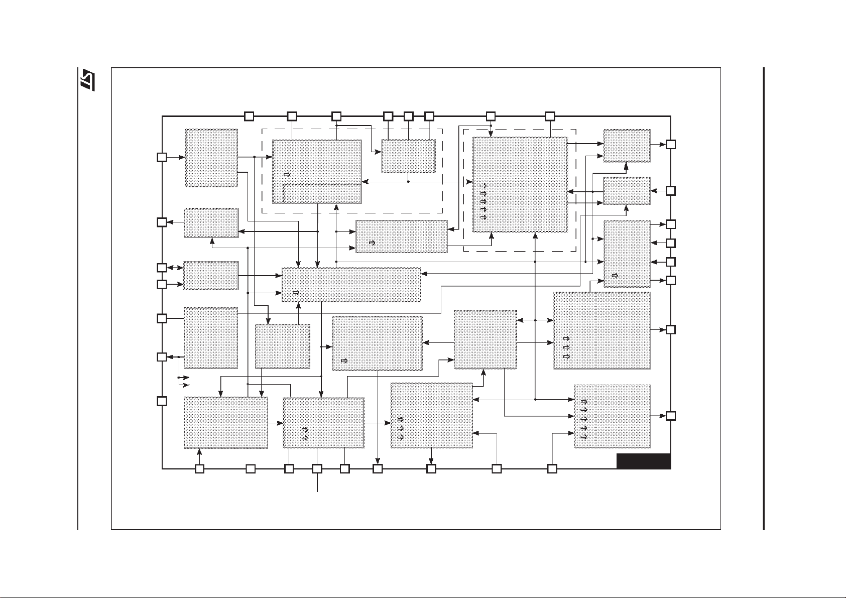
2 - BLOCK DIAGRAM
H/HVSyn
HLckVBk
SDA
SCL
Vcc
RefOut
GND
HGND
7
HPosF
10
HPLL1F
9
R0
HOscF
C0
4
6
8
HFly
12
H-sync
1
detection
Polarity
handling
Phase/frequency
comparator
Horizontal position
Lock detection
3
V-blank
H-lock
31
30
I2C Bus
interface
2
C Bus registers
I
: Functions controlled via I2C Bus
Horizontal
VCO
PLL1
H-moiré controller
H-moiré amplitude
Phase comparator
Phase shifter
H duty controller
Pin cushion asymm.
Parallelogram
Top corner asymm.
Bottom corner asymm.
Hor. duty cycle
HPLL2C
5
PLL2
H-drive
buffer
Safety
processor
B+
DC/DC
converter
controller
B+ ref.
26
25
28
16
15
14
HOut
XRay
BOut
BIsense
BRegIn
BComp
HV-dynamic
29
13
27
Supply
supervision
Reference
generation
Internal
ref.
V-sync detection
Input selection
Polarity handling
V-sync
extraction
& detection
Vertical oscillator
with AGC
S-correction
C-correction
V-dynamic
correction
(focus, bright.)
VDyCor amplitude
Geometry
tracking
V-ramp control
Tracking EHT
Vertical size
Vertical position
Vertical moiré
correction
(focus,brightness)
HVDyCor V-amplitude
HVDyCor H-amplitude
HVDyCor H-symmetry
EW generator
H size
Pin cushion
Keystone
Top corners
Bottom corners
11
HVDyCor
24
EWOut
5/49
2
VSyn
21
VGND
19
VOscF
20 22
VAGCCap
VCap
32
VDyCor
23
VOut
18
VEHTIn
17
HEHTIn
TDA9112
TDA9112
TDA9112
3 - PIN FUNCTION REFERENCE
Pin Name Function
1 H/HVSyn TTL compatible Horizontal /Horizontal and Vertical Sync. input
2 VSyn TTL compatible Vertical Sync. input
3 HLckVBk Horizontal PLL1 Lock detection and Vertical early Blanking composite output
4 HOscF High Horizontal Oscillator sawtooth threshold level Filter input
5 HPLL2C Horizontal PLL2 loop Capacitive filter input
6 CO Horizontal Oscillator Capacitor input
7 HGND Horizontal section GrouND
8 RO Horizontal Oscillator Resistor input
9 HPLL1F Horizontal PLL1 loop Filter input
10 HPosF Horizontal Position Filter and soft-start time constant capacitor input
11 HVDyCor Horizontal and Vertical Dynamic Correction output
12 HFly Horizontal Flyback input
13 RefOut Reference voltage Output
14 BComp B+ DC/DC error amplifier (Comparator) output
15 BRegIn Regulation feedback Input of the B+ DC/DC converter controller
16 BISense B+ DC/DC converter current (I) Sense input
17 HEHTIn Input for compensation of Horizontal amplitude versus EHT variation
18 VEHTIn Input for compensation of Vertical amplitude versus EHT variation
19 VOscF Vertical Oscillator sawtooth low threshold Filter (capacitor to be connected to VGND)
20 VAGCCap Input for storage Capacitor for Automatic Gain Control loop in Vertical oscillator
21 VGND Vertical section GrouND
22 VCap Vertical sawtooth generator Capacitor
23 VOut Vertical deflection drive Output for a DC-coupled output stage
24 EWOut E/WOutput
25 XRay X-Ray protection input
26 HOut Horizontal drive Output
27 GND Main GrouND
28 BOut B+ DC/DC converter controller Output
29 Vcc Supply voltage
30 SCL I
31 SDA I
32 VDyCor Vertical Dynamic Correction output
2
C bus Serial CLock Input
2
C bus Serial DAta input/output
6/49
TDA9112
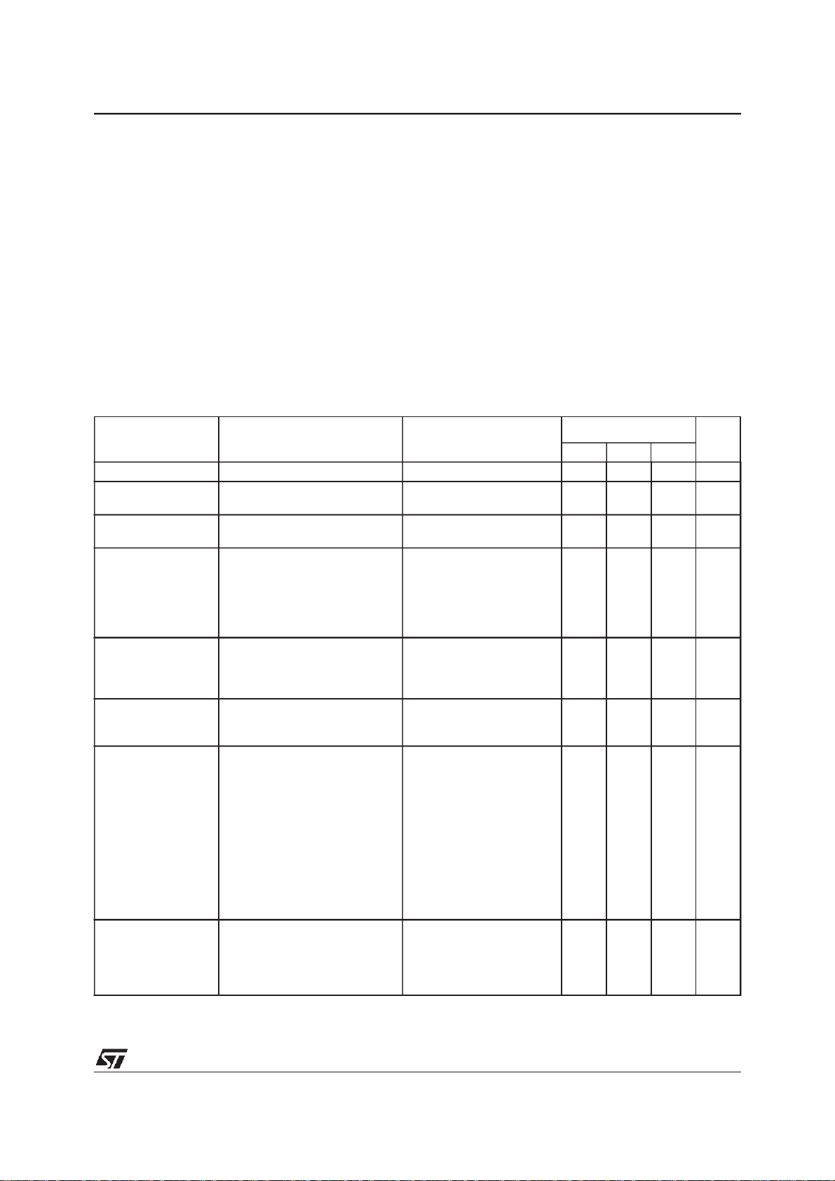
4 - QUICK REFERENCE DATA
Characteristic Value Unit
General
Package SDIP 32
Supply voltage 12 V
Supply current 65 mA
Application category High-end
Means of control/Maximum clock frequency I
EW drive Yes
DC/DC converter controller Yes
Horizontal section
Frequency range 15 to 150 kHz
Autosync frequency ratio (can be enlarged in application) 4.28
Positive/Negative polarity of horizontal sync signal/Automatic adaptation Yes/Yes/Yes
Duty cycle range of the drive signal 30 to 65 %
Position adjustment range with respect to H period ±10 %
Soft start/Soft stop feature Yes/Yes
Hardware/Software PLL lock indication Yes/Yes
Parrallelogram Yes
Pin cushion asymmetry correction (also called Side pin balance) Yes
Top/Bottom/Common corner asymmetry correction Yes/Yes/No
Tracking of asymmetry corrections with vertical size & position Yes
Horizontal moiré cancellation (int.) for Combined/Separated architecture Yes/Yes
Vertical section
Frequency range 35 to 200 Hz
Autosync frequency range (150nF at VCap and 470nF at VAGCCap) 50 to 180 Hz
Positive/Negative polarity of vertical sync signal/Automatic adaptation Yes/Yes/Yes
S-correction/C-correction/Super-flat tube characteristic Yes/Yes/Yes
Vertical size/Vertical position adjustment Yes/Yes
Vertical moiré cancellation (internal) Yes
Vertical breathing compensation Yes
EW section
Pin cushion correction Yes
Keystone correction Yes
Top/Bottom/Common corner correction Yes/Yes/No
Horizontal size adjustment Yes
Tracking of EW waveform with Frequency/Vertical size & position Yes/Yes
Breathing compensation on EW waveform Yes
Dynamic correction section (dyn. focus, dyn. brightness,...)
Vertical dynamic correction output VDyCor Yes
Horizontal dynamic correction output HDyCor No
Composite HV dynamic correction output HVDyCor Yes
Tracking of horizontal waveform component with Horizontal size/EHT Yes/Yes
Tracking of vertical waveforms (component) with V. size & position Yes
DC/DC controller section
Step-up/Step-down conversion mode Yes/Yes
Internal/External sawtooth configuration Yes/Yes
Bus-controlled output voltage Yes
Soft start/Soft stop feature Yes/Yes
Positive (N-MOS)/Negative(P-MOS) polarity of BOut signal Yes/Yes
2
C Bus/400 kHz
7/49
TDA9112
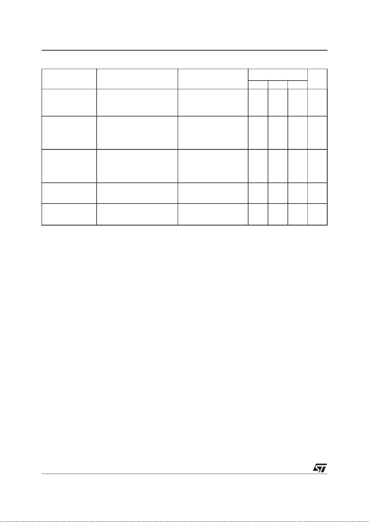
5 - ABSOLUTE MAXIMUM RATINGS
All voltages are given with respect to ground.
Currents flowing from the device (sourced)are signed negative. Currents flowing tothe device aresigned
positive.
Symbol Parameter
V
CC
Supply voltage (pin Vcc) -0.4 13.5 V
Pins HEHTIn, VEHTIn, XRay, HOut, BOut
Pins H/HVSyn, VSyn, SCL, SDA
V
(pin)
Pins HLckVBk, CO, RO, HPLL1F, HPosF, HVDyCor, BRegIn,
BISense, VAGCCap, VCap, VDyCor, HOscF, VOscF
Pin HPLL2C
Pin HFly
V
T
ESD
stg
T
j
ESD susceptibility
(human body model: discharge of 100pF through 1.5kΩ) -2000 2000 V
Storage temperature -40 150 °C
Junction temperature 150 °C
Value
Min Max
V
V
5.5
V
RefO
RefO
V
RefO
CC
-0.4
-0.4
-0.4
-0.4
-0.4
Unit
V
V
V
/2
V
V
8/49
TDA9112
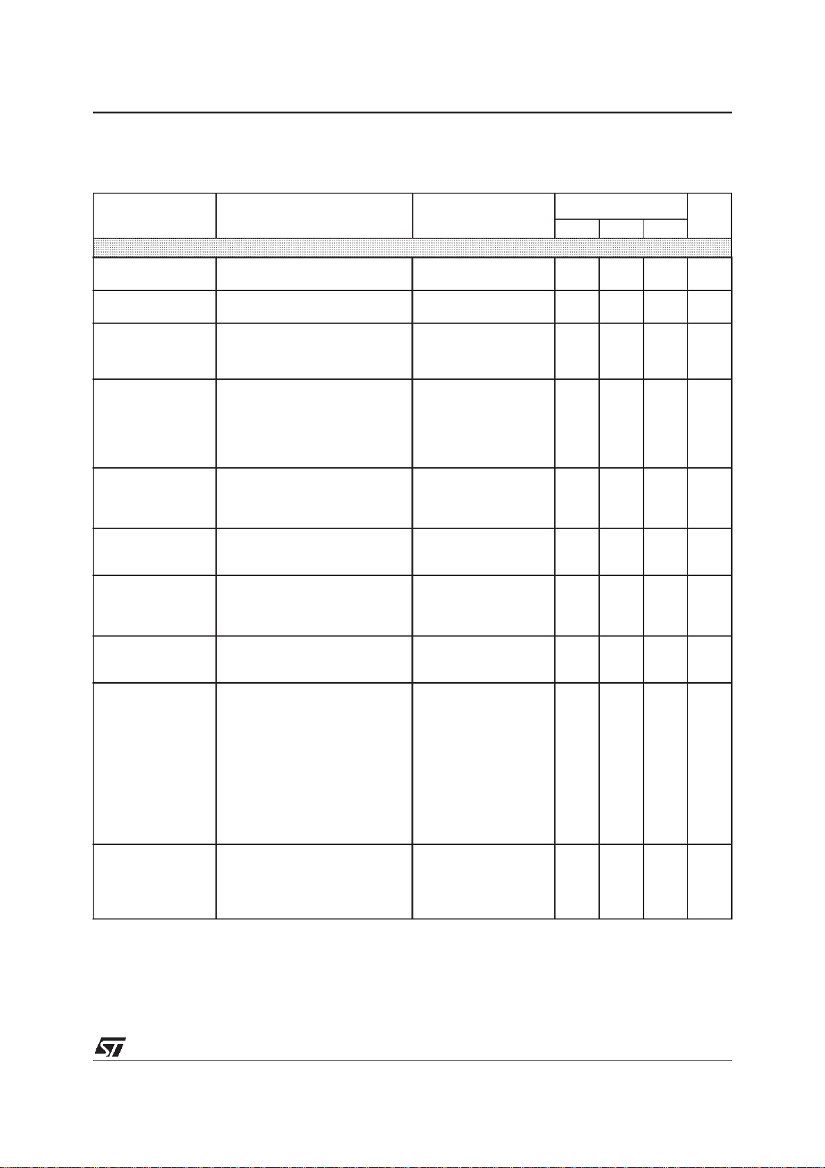
6 - ELECTRICAL PARAMETERS AND OPERATING CONDITIONS
Medium (middle) value of an I2C Bus control or adjustment register composed of bits D0, D1,...,Dn is the
one having Dn at ”1” and all other bits at ”0”. Minimum value is the one with all bits at 0, maximum value
is the one with all at ”1”.
Currents flowing from the device (sourced)are signed negative. Currents flowing tothe device aresigned
positive.
THis period of horizontal deflection.
6.1 - THERMAL DATA
Symbol Parameter
T
R
amb
th(j-a)
Operating ambient temperature 0 70 °C
Junction-ambience thermal resistance 65 °C/W
6.2 - SUPPLY AND REFERENCE VOLTAGES
T
=25°C
amb
Symbol Parameter Test Conditions
V
V
I
RefO
CC
I
CC
RefO
Supply voltage at Vcc pin 10.8 12 13.2 V
Supply current to Vcc pin VCC=12V 65 mA
Reference output voltage at RefOut pin VCC=12V,I
Current sourced by RefOutoutput -5 0 mA
6.3 - SYNCHRONIZATION INPUTS
Vcc = 12V, T
Symbol Parameter Test Conditions
V
LoH/HVSyn
V
HiH/HVSyn
V
LoVSyn
V
HiVSyn
R
PdSyn
t
PulseHSyn
t
PulseHSyn/TH
t
PulseVSyn
t
PulseVSyn/TV
t
extrV/TH
t
HPolDet
=25°C
amb
LOW level voltage on H/HVSyn 0 0.8 V
HIGH level voltage on H/HVSyn 2.2 5 V
LOW level voltage on VSyn 0 0.8 V
HIGH level voltage on VSyn 2.2 5 V
Internal pull-down on H/HVSyn, VSyn 100 175 250 kΩ
H sync. pulse duration on H/HVSyn pin 0.5 µs
Proportion of H sync pulse to H period Pin H/HVSyn 0.2
V sync. pulse duration Pins H/HVSyn, VSyn 0.5 750 µs
Proportion of V sync pulse to V period Pins H/HVSyn, VSyn 0.15
Proportion of sync pulse length to H peri-
od for extraction as V sync pulse
Pin H/HVSyn,
cap. on pin CO = 820pF
Polarity detection time (after change) Pin H/HVSyn 0.75 ms
Value
Value
Min. Typ. Max.
= -2mA 7.65 8.0 8.2 V
RefO
Value
Min. Typ. Max.
0.21 0.3
Unit
Units
Units
9/49
TDA9112
6.4 - HORIZONTAL SECTION
Vcc = 12V, T
amb
=25°C
Symbol Parameter Test Conditions
PLL1
I
RO
C
CO
f
HO
f
HO(0)
f
HOCapt
f
∆
HO 0()
-----------------------------
f
HO 0()
∆f
/∆V
HO
V
HO
V
HOThrfr
V
HPosF
Current load on RO pin 1.5 mA
Capacitance on CO pin 390 pF
Frequency of hor. oscillator 150 kHz
Free-running frequency of hor. oscill.
Hor. PLL1 capture frequency
(4)
Temperature drift of free-running freq.
(1)
RRO=5.23kΩ,CCO=820pF 27 28.5 29.9 kHz
f
= 28.5kHz 29 122 kHz
HO(0)
(3)
T∆⋅
Average horizontal oscillator sensitivity f
HO
H. oscill. control voltage on pin HPLL1F V
Threshold on H. oscill. control voltage on
HPLL1F pin for tracking of EW with freq.
Control voltage on HPosF pin
= 28.5kHz 19.6 kHz/V
HO(0)
=8V 1.4 6.0 V
RefO
V
=8V 5.0 V
RefO
HPOS
(Sad01):
11111111b
10000000b
00000000b
V
HOThrLo
V
HOThrHi
Bottom of hor. oscillator sawtooth
Top of hor. oscillator sawtooth
(6)
(6)
PLL2
R
In(HFly)
I
InHFly
V
ThrHFly
V
S(0)
V
BotHPLL2C
V
TopHPLL2C
(min)/T
t
ph
(max)/T
t
ph
Input impedance on HFly input V
(HFly)>VThrHFly
Current into HFly input At top of H flyback pulse 5 mA
Voltage threshold on HFly input 0.6 0.7 V
H flyback lock middle point
Low clamping voltage on HPLL2C pin
High clamping voltage on HPLL2C pin
Min. advance of H-drive OFF before
H
middle of H flyback
Max. advance of H-drive OFF before
H
middle of H flyback
(7)
(8)
(6)
No PLL2 phase modulation
(5)
(5)
Null asym. correction 0 %
Null asym. correction 44 %
H-drive output on pin HOut
I
HOut
t
Hoff/TH
Current into HOut output Output driven LOW 30 mA
HDUTY
Duty cycle of H-drive signal
(Sad00):
x1111111b
x0000000b
Soft-start/Soft-stopvalue
Picture geometry corrections through PLL1 & PLL2
HPOS
(Sad01):
11111111b
00000000b
t
Hph/TH
H-flyback (centre) static phase vs. sync
signal (via PLL1), see Figure 7
(2)
Value
Units
Min. Typ. Max.
-150 ppm/°C
2.6
3.2
3.8
2.8
3.4
4.0
3.0
3.6
4.2
1.6 V
6.4 V
300 500 700 Ω
4.0 V
1.6 V
3.9 4.05 4.2 V
27
65
85
+11
-11
V
V
V
%
%
%
%
%
10/49
TDA9112
Symbol Parameter Test Conditions
Value
Units
Min. Typ. Max.
PCAC
(Sad11h) full span
(9)
VPOS
VSIZE
VSIZE
VSIZE
PARAL
(9)
VPOS
VSIZE
VSIZE
VSIZE
VPOS
VSIZE
TCAC
(9)
span
VPOS
VSIZE
VSIZE
VSIZE
BCAC
(9)
span
VPOS
VSIZE
VSIZE
VSIZE
at medium
at minimum
at medium
at maximum
(Sad12h) fullspan
at medium
at minimum
at medium
at maximum
at max. or min.
at minimum
(Sad13h) full
at medium
at minimum
at medium
at maximum
(Sad14h) full
at medium
at minimum
at medium
at maximum
±1.0
±1.8
±2.8
±1.75
±2.2
±2.8
±1.75
±0.8
±2.0
±4.4
±0.8
±2.0
±4.4
%
%
%
%
%
%
%
%
%
%
%
%
%
t
PCAC/TH
t
ParalC/TH
t
TCAC/TH
t
BCAC/TH
Contribution of pin cushion asymmetry
correction to phase of H-drive vs. static
phase (via PLL2), measured in corners
Contribution of parallelogram correction
to phase of H-drive vs. static phase (via
PLL2), measured in corners
Contribution of top corner asymmetry
correction to phase of H-drive vs. static
phase (via PLL2), measured in corners
Contribution of bottom corner asymmetry
correction to phase of H-drive vs. static
phase (via PLL2), measured in corners
Note 1: Frequency at no sync signal condition. For correct operation, the frequency of the sync signal applied must
always be higher than the free-running frequency. The application must consider the spread of values of real
electrical components in R
the free-running frequency is f
and CCOpositions so as to always meet this condition. The formula to calculate
RO
=0.12125/(RROCCO)
HO(0)
Note 2: Base of NPN transistor with emitter to ground is internally connected on pin HFly through a series resistance of
about 500Ω and a resistance to ground of about 20kΩ.
Note 3: Evaluated and figured out during the device qualification phase. Informative. Not tested on every single unit.
Note 4: This capture range can be enlarged by external circuitry.
Note 5: The voltage on HPLL2C pin corresponds to immediate phase of leading edge of H-drive signal on HOut pin with
respect to internal horizontal oscillator sawtooth. It must be between the two clamping levels given. Voltage
equal to one of the clamping values indicates a marginal operation of PLL2 or non-locked state.
Note 6: Internal threshold. See Figure 6.
Note 7: Thet
(min)/THparameter is fixed by the application. For correct operation of asymmetry corrections through
ph
dynamic phase modulation, this minimum must be increased by maximum of the total dynamic phase required
in the direction leading to bending of corners to the left. Marginal situation is indicated by reach of V
TopHPLL2C
high clamping level by waveform on pin HPLL2C. Also refer to Note 5 and Figure 6.
Note 8: Thet
(max)/THparameter is fixed by the application. For correct operation of asymmetry corrections through
ph
dynamic phase modulation, this maximum must be reduced by maximum of thetotal dynamic phase required in
the direction leading to bending of corners to the right. Marginal situation is indicated by reach of V
BotHPLL2C
low clamping level by waveform on pin HPLL2C. Also refer to Note 5 and Figure 6.
Note 9: All other dynamic phase corrections of picture asymmetry set to their neutral (medium) positions.
11/49

TDA9112
6.5 - VERTICAL SECTION
VCC= 12V,T
Symbol Parameter Test Conditions
amb
=25°C
Value
Units
Min. Typ. Max.
AGC-controlled vertical oscillator sawtooth; V
R
L(VAGCCap)
V
VOB
V
VOT
t
VODis
f
VO(0)
f
VOCapt
∆
V
VOdev
---------------------------------
V
VOamp
V
∆
--------------------------------
∆
V
--------------------------------
∆
---------------------------------------- -
V
VOampfVO
VOS cor–
V
VOamp
VOC cor–
V
VOamp
V
VOamp
16()
∆⋅
Ext. load resistance on
VAGCCap pin
Sawtooth bottom voltage on
VCap pin
(10)
(11)
Sawtooth top voltage on VCap
pin
Sawtooth Discharge time C
Free-running frequency C
AGC loop capture frequency C
Sawtooth non-linearity
(12)
S-correction range
C-correction range
Frequency drift of sawtooth
amplitude
(17)(18)
Vertical output drive signal (on pin VOut);V
V
mid(VOut)
V
amp
V
offVOut
I
VOut
V
VEHT
V
∆
amp
------------------------------------------
∆⋅
V
ampVVEHT
Middle point on VOut sawtooth
Amplitude of VOut sawtooth
(peak-to-peak voltage)
Level on VOut pin at V-drive ”off” I2Cbit VOutEn at 0 3.8 V
Current delivered by VOut out-
put
Control input voltage range on
VEHTIn pin
Breathing compensation
RefO
=8V
RefO
∆V
amp/Vamp
No load on VOscF pin
AGC loop stabilized
V sync present
No V sync
VCap
VCap
VCap
AGC loop stabilized,
AGC loop stabilized,
tVR=1/4 T
tVR=3/4 T
AGC loop stabilized,
tVR=1/2 T
CCOR
x0000000b
x1000000b
x1111111b
AGC loop stabilized
f
VOCapt
=8V
VPOS
x0000000b
x1000000b
x1111111b 3.65
VSIZE
x0000000b
x1000000b
x1111111b 3.5
V
VEHT>VRefO
V
VEHT
(R=∞) ≤1% 65 MΩ
(11)
1.85 1.95 2.1 V
5
4.9
V
V
=150nF 80 µs
=150nF 100 Hz
=150nF 50 185 Hz
(15)
VR
VR
(15)
VR
(Sad0A):
(min)≤f
VO≤fVOCapt
(12)
(13)
(14)
(max) 200
0.5 %
-5
+5
-3
0
+3
ppm/Hz
%
%
%
%
%
(Sad08):
3.2
3.5
3.8
3.3 V
V
V
(Sad07):
2.25
3.0
3.75
2.5 V
V
V
-5 5 mA
(min)≤V
VEHT≤VRefO
1 V
0
2.5
RefO
V
%/V
%/V
Note 10: Value of acceptable cumulated parasitic load resistance due to humidity, AGC storage capacitor leakage, etc.,
for less than 1% of V
amp
change.
12/49
TDA9112
Note 11: The threshold for V
influence the value of V
is generated internally and routed to VOscF pin. Any DC current on this pin will
VOB
VOB
.
Note 12: Maximum of deviation from an ideally linear sawtooth ramp at null
CCOR
(Sad0A at x1000000b). The same rate applies to V-drive signal on VOut pin.
SCOR
Note 13: Maximum
Note 14: Null
Note 15: ”t
SCOR
” is time from the beginning ofvertical ramp of V-drive signal on VOut pin. ”TVR” is the duration ofthis ramp,
VR
(Sad09 at x1111111b), null
(Sad09 at x0000000b).
CCOR
(Sad0A at x1000000b).
see chapter TYPICAL OUTPUT WAVEFORMS and Figure 16.
Note 16: V
VOamp
= V
VOT-VVOB
Note 17: The same rate applies to V-drive signal on VOut pin.
Note 18: Informative, not tested on each unit.
6.6 - EW DRIVE SECTION
VCC= 12V, T
Symbol Parameter Test Conditions
V
EW
I
EWOut
V
HEHT
V
EW-DC
V
∆
EW DC–
-----------------------------
∆
V
HEH T
V
∆
EW DC–
-------------------------------------
V
EW DC–
V
EW-PCC
V
EW PCC–
--------------------------------------------------------
EW PC C–
tvrTVR=[]
=25°C
amb
Output voltage on EWOut pin 1.8 6.5 V
Current sourced by EWOut out-
put
Control voltage range on HEH-
TIn pin
DC component of the EW-drive
signal on EWOut pin
Breathing compensation on
V
Temperature drift of DC component of the EW-drive signal on
T∆⋅
EWOut pin
Pin cushion correction component of the EW-drive signal on
EWOut pin
tvr0=[]
Tracking of PCC component of
the EW-drive signalwith vertical
position adjustment
EW-DC
(19)(22)(23)(30)
tVR=1/2 T
HSIZE
VR
(Sad10h):
00000000b
10000000b
11111111b
(19)(20)(21)(22)
tVR=1/2 T
V
HEHT>VRefO
V
HEHT
(18)(19)(21)(23)(30)
tVR=1/2 T
(19)(20)(21)(23)(24)(25)
(26)(30)
VSIZE
PCC
(15)
VR
(min)≤V
VR
at maximum
(Sad0C):
x0000000b
x1000000b
x1111111b
Tracking with
PCC
at x1000000b
VSIZE
(Sad07):
x0000000b
x1000000b
(19)(20)(21)(24)(27)(29)(30)
PCC
at x1111111b
VPOS
(Sad08):
x0000000b
x1111111b
SCOR
(15)
HEHT≤VRefO
(15)
VSIZE
:
(Sad09 at x0000000b) and null
Value
Min. Typ. Max.
-1.5 0 mA
1 V
RefO
2
3.25
4.5
0
-0.125
100 ppm/°C
0
0.7
1.5
0.25
0.5
0.52
1.92
Units
V
V
V
V
V/V
V/V
V
V
V
V
V
13/49
TDA9112
Symbol Parameter Test Conditions
Value
Units
Min. Typ. Max.
Keystone correction component
V
EW-Key
of the EW-drive signal on
EWOut pin
Top corner correction compo-
V
EW-TCor
nent of the EW-drive signal on
EWOut pin
Bottom corner correction compo-
V
EW-BCor
V
∆
EW
---------------------------------
∆⋅
V
EWVHO
V
∆
EW AC–
-----------------------------------------------------
V
EW AC–
Note 19:
Note 20:
Note 21:
Note 22:
Note 23:
Note 24:
V
∆⋅
KEYST
TCC
at medium (neutral) value.
BCC
at medium (neutral) value.
PCC
at minimum value.
VPOS
HSIZE
HEH T
nent of the EW-drive signal on
EWOut pin
Tracking of EW-drive signal with
horizontal frequency
Breathing compensation on
(31)
V
EW-AC
at medium (neutral) value.
at medium (neutral) value.
at minimum value.
Note 25: Defined as difference of (voltage at t
Note 26: Defined as difference of (voltage at t
Note 27:
Note 28: Difference (voltage at t
VSIZE
at maximum value.
=0) minus (voltage at tVR=TVR).
VR
(32)
=0) minus (voltage at tVR=1/2 TVR).
VR
VR=TVR
(20)(21)(22)(23)(24)(27)(28)(30)
KEYST
(Sad0D):
x0000000b
x1111111b
(19)(21)(22)(23)(24)(25)(27)(30)
TCC
(Sad0E):
x0000000b
x1000000b
x1111111b
(19)(20)(22)(23)(24)(26)(27)(30)
BCC
(Sad0F):
x0000000b
x1000000b
x1111111b
VHO>V
HOThrfr
VHO(min)≤VHO≤V
(25)(26)
V
HEHT>VRefO
V
(min)≤V
HEHT
HOThrfr
HEHT≤VRefO
) minus (voltage at tVR=1/2 TVR).
0.4
-0.4
-1.25
0
+1.25
-1.25
0
+1.25
0
-27
0
1.75
Note 29: Ratio ”A/B”of parabola component voltage at tVR=0 versus parabola component voltage at tVR=TVR.
See Figure 2.
Note 30: V
Note 31: V
HEHT>VRefO
EW-AC
, V
VEHT>VRefO
is sum of all components other than V
(contribution of PCC, keystone correction and corner
EW-DC
corrections).
Note 32: More precisely tracking with voltage on HPLL1F pin which itself depends on frequency at a rate given by
external components on PLL1 pins.
V
V
V
V
V
V
V
V
%/V
%/V
%/V
%/V
14/49
6.7 - DYNAMIC CORRECTION OUTPUTS SECTION
TDA9112
VCC= 12V, T
amb
=25°C
Symbol Parameter Test Conditions
Composite Horizontal and Vertical Dynamic Correction output HVDyCor
I
HVDyCor
V
HVD-DC
V
∆
HVD DC–
--------------------------------------- -
V
HVD DC–
V
HVD-H
Current delivered by HVDyCor
output
DC component of the drive signal
on HVDyCor output
Temperature drift of DCcomponent
of the drive signal on HVDyCor
T∆⋅
Amplitude of H-parabola component of the drive signal on HVDyCor output
R
L(HVDyCor)
(18)
(33)(34)
=10kΩ 2.1 V
HDyCorTr Off
HVDC-HAMP
x0000000b
x1000000b
x1111111b
V
constant
V
HVD H–
------------------------------------------------------
V
HVD H–
V
HVD H–
---------------------------------------------------------- -
V
HVD H–
TrHSOn[]
TrHSOff[]
TrEHTOn[]
TrEHTOff[]
t
HVD-Hoffset/TH
Impact of horizontal size adjustment on HVDyCor H-parabola
component (tracking)
(35)
Impact of voltage on HEHTIninput
on HVDyCor H-parabola compo-
(36)
nent
Offset (phase) of H-parabola com-
ponent of the drive signal on HVDyCor output
(38)
HEHT
HSIZE
(Sad10h):
00000000b
11111111b
HSIZE
constant
V
HEHT>VRefO
V
HEHT=VRefO
HVDC-HSYM
x0000000b
x1000000b
x1111111b
-4V
(39)
Duration of the flat part at the start
t
HVD-Hflat
of H-parabola component of the
drive signal on HVDyCor output
fHO=31kHz 500 ns
(38)
(23)
VSIZE
at x1000000b
HVDC-VAMP
x0000000b
V
HVD-V
Amplitude of V-parabola component of the drive signal on HVDyCor output
x1000000b
x1111111b
HVDC-VAMP
mum
VSIZE
(Sad07):
x0000000b
x1111111b
HVDC-VAMP
V
HVD V–tvr
------------------------------------------------------
V
HVD V–tvrTVR
0=[]
=[]
Tracking of V-parabola component
of thedrive signal on HVDyCor output with vertical position
(37)
mum
VPOS
(Sad08):
x0000000b
x1111111b
(Sad04):
(Sad05):
(Sad06):
at maxi-
at maxi-
Value
Min. Typ. Max.
-2 0 mA
200 ppm/°C
3.7
1.5
0.9
2
(1.34)
1
1
2
(1.07)
+24.5
0
-24.5
0
0.5
1
0.5
1.6
0.52
1.92
Units
V
V
V
%
%
%
V
V
V
V
V
15/49
 Loading...