

TDA9109/N
LOW-COST DEFLECTIONPROCESSOR
FOR MULTISYNC MONITORS
HORIZONTAL
.
SELF-ADAPTATIVE
.
DUALPLLCONCEPT
.
150kHzMAXIMUM FREQUENCY
.
X-RAYPROTECTIONINPUT
.
I2C CONTROLS : H-POSITION, FREQUENCY
GENERATORFOR BURN-IN MODE
VERTICAL
.
VERTICALRAMP GENERATOR
.
50 TO165Hz AGC LOOP
.
GEOMETRYTRACKINGWITHVPOS& VAMP
.
I2C CONTROLS:
VAMP, VPOS, S-CORR, C-CORR
.
DC BREATHING COMPENSATION
2
C GEOMETRYCORRECTIONS
I
.
VERTICALPARABOLAGENERATOR
(Pincushion,Keystone)
.
HORIZONTALDYNAMICPHASE
(SidePin Balance& Parallelogram)
.
HORIZONTALAND VERTICALDYNAMIC FOCUS (Horizontal Focus Amplitude, Horizontal
FocusSymmetry,VerticalFocus Amplitude)
GENERAL
.
SYNCPROCESSOR
.
12V SUPPLYVOLTAGE
.
8V REFERENCEVOLTAGE
.
HOR.& VERT. LOCK/UNLOCK OUTPUTS
.
READ/WRITEI2C INTERFACE
.
VERTICALMOIRE
.
B+REGULATOR
- INTERNAL PWM GENERATOR FOR B+
CURRENT MODE STEP-UP CONVERTER
- S WITCHABL E TO STEP-DOWN CONVERTER
2
CADJUSTABLEB+REFERENCE VOLTAGE
-I
- OUTPUT PULSES SYNCHRONIZED ON
HORIZONTALFREQUENCY
- INTERNALMAX. CURRENT LIMITATION
.
COMPARED WITH THE TDA9109,
THE TDA9109/NHAS:
2
-NOI
- FIXED HORIZONTALDUTY CYCLE (48%)
- INCREASEDMAX.STORAGETIME OF THE
C FREE RUNNING FREQUENCY AD-
JUSTMENT
HORIZONTALSCANNING TRANSISTOR
DESCRIPTION
The TDA9109/N is a monolithic integrated circuit
assembledin32-pinshrinkdual in lineplasticpackage.ThisIC controlsall thefunctionsrelatedtothe
horizontal and vertical deflection in multimode or
multi-frequencycomputerdisplaymonitors.
The internal sync processor, combined with the
very powerful geometrycorrection block makethe
TDA9109/N suitable for very high performance
monitors,using very few externalcomponents.
Thehorizontaljitter levelisverylow.Itisparticularly
well suited forhigh-end 15” and 17” monitors.
Combined with the ST7275Microcontroller family,
TDA9206 (Video preamplifier) and STV942x (OnScreen Display controller) the TDA9109/N allows
2
Cbus controlled computer display monitors
fullyI
to be built with a reduced number of external
components.
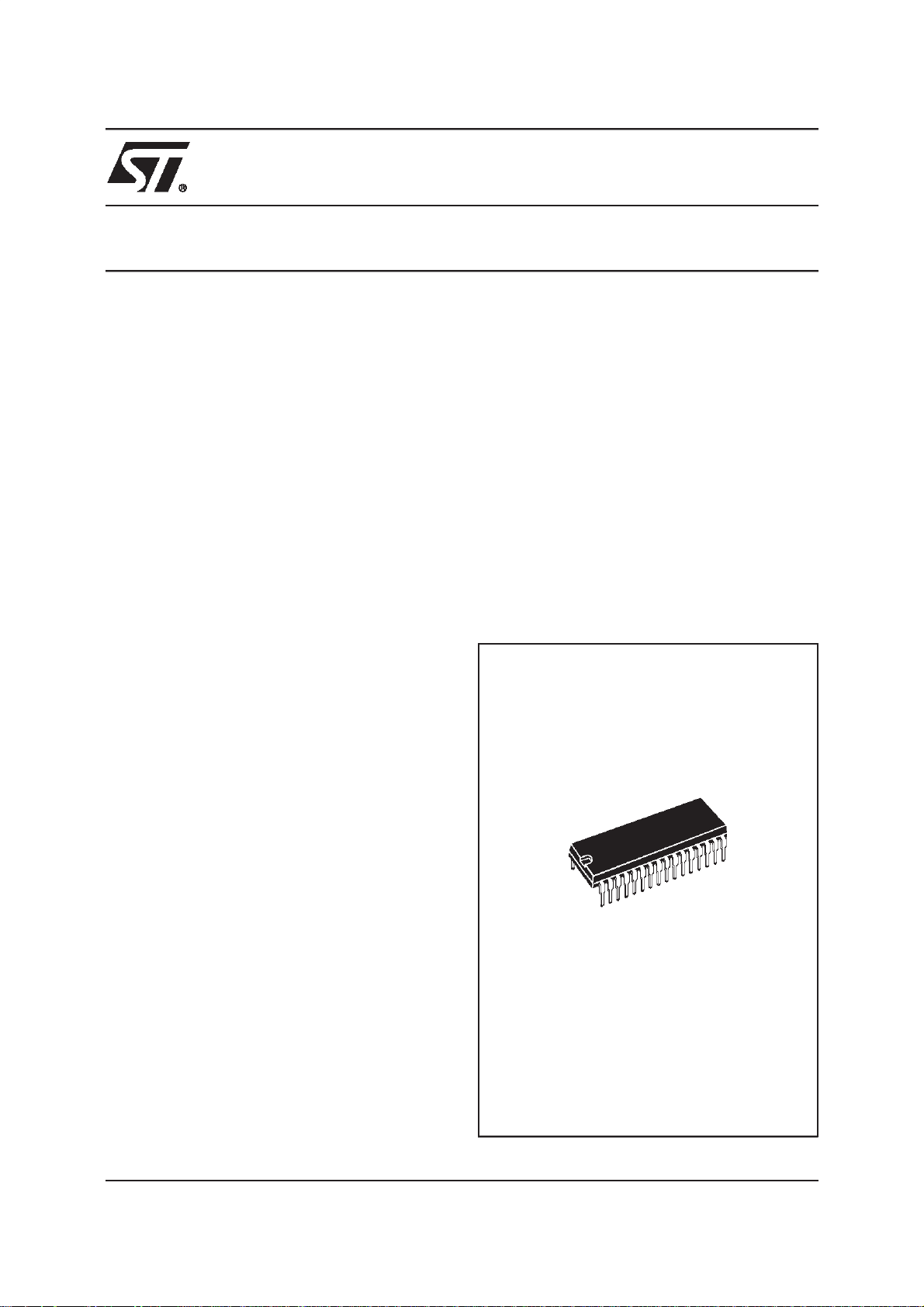
SHRINK32
(Plastic Package)
ORDER CODE : TDA9109/N
June 1998
1/32
TDA9109/N
PIN CONNECTIONS
H/HVIN
VSYNCIN
HLOCKOUT
PLL2C
C0
R0
PLL1F
HPOSITION
HFOCUSCAP
FOCUS-OUT
HGND
HFLY
HREF
COMP
REGIN
SENSE
1
2
3
4
5
6
7
8
9
10
11
12
13
14
15
16
32
31
30
29
28
27
26
25
24
23
22
21
20
19
18
17
5V
SDA
SCL
V
CC
BOUT
GND
HOUT
XRAY
EWOUT
VOUT
VCAP
V
REF
VAGCCAP
VGND
BREATH
B+GNDI
9109N-01.EPS
2/32
TDA9109/N
PIN CONNECTIONS
Pin Name Function
1 H/HVIN TTL compatible Horizontal sync Input (separate or composite)
2 VSYNCIN TTL compatible Vertical sync Input (for separated H&V)
3 HLOCKOUT First PLL Lock/Unlock Output (0V unlocked - 5V locked)
4 PLL2C Second PLL LoopFilter
5 C0 Horizontal Oscillator Capacitor
6 R0 Horizontal Oscillator Resistor
7 PLL1F First PLL Loop Filter
8 HPOSITION HorizontalPosition Filter (capacitor to be connected to HGND)
9 HFOCUSCAP Horizontal Dynamic Focus Oscillator Capacitor
10 FOCUSOUT Mixed Horizontal and Vertical Dynamic Focus Output
11 HGND Horizontal Section Ground
12 HFLY Horizontal Flyback Input (positivepolarity)
13 HREF Horizontal Section ReferenceVoltage (to be filtered)
14 COMP B+ Error Amplifier Output for frequency compensation and gain setting
15 REGIN Regulation Input of B+ control loop
16 I
SENSE
17 B+GND Ground (related toB+ reference adjustment)
18 BREATH DC Breathing Input Control (compensation of vertical amplitude against EHV variation)
19 VGND Vertical Section Ground
20 VAGCCAP Memory Capacitor for Automatic Gain Control Loop in Vertical Ramp Generator
21 V
REF
22 VCAP Vertical Sawtooth Generator Capacitor
23 VOUT Vertical Ramp Output(withfrequencyindependantamplitude and S or C Correctionsif any).
24 EWOUT Pin Cushion - E/W Correction Parabola Output
26 HOUT Horizontal Drive Output (internal transistor, open collector)
25 XRAY X-RAY protection input (with internal latch function)
27 GND General Ground (referenced to V
28 BOUT B+ PWMRegulator Output
29 V
CC
30 SCL I
31 SDA I
32 5V Supply Voltage (5V typ.)
Sensing ofexternal B+ switching transistor current, or switch for step-down converter
Vertical Section Reference Voltage (to be filtered)
It is mixed with vertical position voltage and vertical moiré.
)
CC
Supply Voltage (12V typ)
2
C Clock Input
2
C Data Input
9109N-01.TBL
3/32
TDA9109/N
QUICK REFERENCE DATA
Parameter Value Unit
Horizontal Frequency 15 to 150 kHz
Autosynch Frequency (for given R0 and C0) 1 to 4.5 f0
æ Horizontal Sync Polarity Input YES
Polarity Detection (on bothHorizontal and Vertical Sections) YES
TTL Composite Sync YES
Lock/Unlock Identification (on both Horizontal 1st PLL and Vertical Section) YES
2
C Control for H-Position
I
XRAY Protection YES
2
C Horizontal Duty Cycle 48 %
Fixed I
2
C Free Running Frequency Adjustment NO
I
Stand-by Function YES
Dual Polarity H-Drive Outputs NO
Supply Voltage Monitoring YES
PLL1 Inhibition Possibility NO
Blanking Outputs NO
Vertical Frequency 35 to 200 Hz
Vertical Autosync (for 150nF on Pin 22 and 470nF on Pin 20) 50 to 165 Hz
Vertical S-Correction YES
Vertical C-Correction YES
Vertical Amplitude Adjustment YES
DC Breathing Control on VerticalAmplitude YES
Vertical Position Adjustment YES
East/West (E/W) Parabola Output (also known as Pin Cushion Output) YES
E/W Correction Amplitude Adjustment YES
Keystone Adjustment YES
Internal Dynamic Horizontal Phase Control YES
Side Pin Balance Amplitude Adjustment YES
Parallelogram Adjustment YES
Tracking of Geometric Corrections with Vertical Amplitude and Position YES
Reference Voltage (both on Horizontal and Vertical) YES
Dynamic Focus (both Horizontal and Vertical) YES
2
C Horizontal Dynamic Focus Amplitude Adjustment YES
I
2
C Horizontal Dynamic Focus Symmetry Adjustment YES
I
2
C Vertical Dynamic Focus Amplitude Adjustment YES
I
Detection of Input Sync Type (biased from 5V alone) YES
Vertical Moiré Output YES
2
C Controlled V-Moiré Amplitude YES
I
Frequency Generator for Burn-in YES
2
C Read/Write 400 kHz
Fast I
B+ Regulation adjustable by I
2
C YES
10 %
±
9109N-02.TBL
4/32
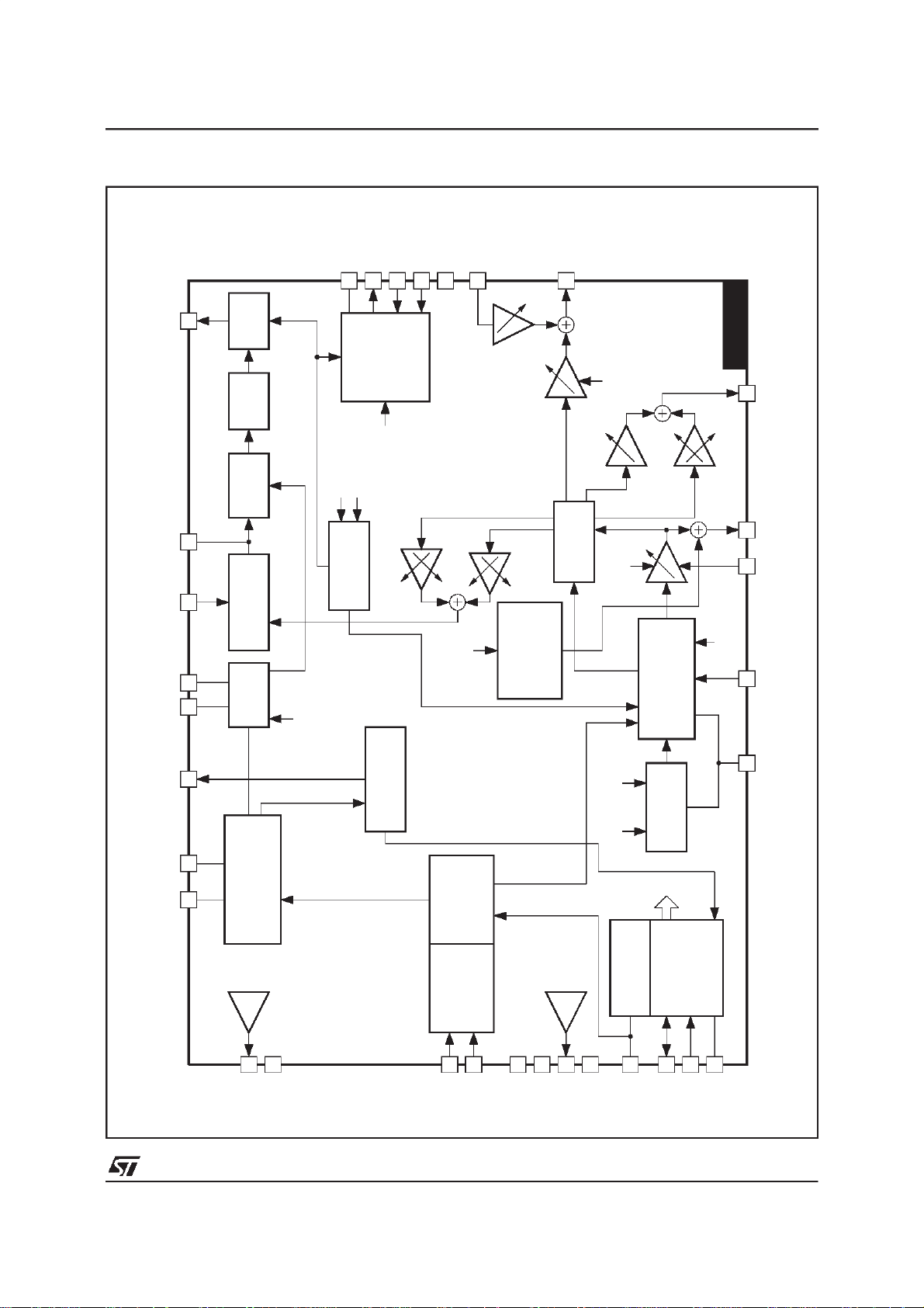
BLOCKDIAGRAM
TDA9109/N
HOUT
PLL2C
HFLY
C0
R0
HLOCKOUT
4
5
67 26
3
HOUT
BUFFER
(48%)
H-DUTY
PHASE
SHIFTER
PHASE
COMPARATOR
VCO
2 bits
Forced
Frequency
28 B+OUT
14 COMP
B+
B+ Adjust
CC
XRAY
V
SAFETY
PROCESSOR
SENSE
BGND
I
17
16
15 REGIN
CONTROLLER
7 bits
2
X
Spin Bal
HFOCUSCAP
9
2
6 bits
X
VSYNC
2
X
2 x 5 bits
Amp & Symmetry
6 bits
Parallelogram
MOIRE
CANCEL
VERTICAL
5 BITS+ON/OFF
10 FOCUS
VAMPVDF
E/W
7 bits
TRACKING
GEOMETRY
VAMP
6 bits
2
X
7 bits
X
6 bits
Keyst.
VERTICAL
OSCILLATOR
RAMP GENERATOR
TDA9109/N
EWOUT
V
OUT
BREATH
18
7 bits
VPOS
V
AGCCAP
20
V
CAP
22 23
HPOSITION
PLL1F
LOCK/UNLOCK
IDENTIFICATION
6 bits 6 bits
S AND C
CORRECTION
8
COMPARATOR
H-PHASE(7 bits)
PHASE/FREQUENCY
SYNC
PROCESSOR
RESET
REF
V
131211
HREF
HGND
SELECT
SYNC INPUT
1
H/HVIN
(1 bit)
2
VSYNCIN
29
V
REF
V
21
25
CC
XRAY
REF
V
GENERATOR
192432
5V
VGND
C INTERFACE
2
I
30
31
SCL
SDA
27
GND
9109N-02.EPS
5/32

TDA9109/N
ABSOLUTE MAXIMUMRATINGS
Symbol Parameter Value Unit
V
V
V
VESD
T
T
THERMAL DATA
Symbol Parameter Value Unit
R
th (j-a)
SYNC PROCESSOR
OperatingConditions (V
Symbol Parameter Test Conditions Min. Typ. Max. Unit
HsVR Voltage on H/HVIN Input Pin 1 0 5 V
MinD Minimum Horizontal Input Pulses Duration Pin 1 0.7 µs
Mduty Maximum Horizontal Input Signal Duty Cycle Pin 1 25 %
VsVR Voltage on VSYNCIN Pin2 0 5 V
VSW Minimum Vertical Sync Pulse Width Pin 2 5 µs
VSmD Maximum Vertical SyncInput Duty Cycle Pin 2 15 %
VextM Maximum Vertical Sync Widthon TTLH/Vcomposite Pin 1 750
I
HLOCKOUT
Supply Voltage (Pin 29) 13.5 V
CC
Supply Voltage (Pin 32) 5.7 V
DD
Max Voltage on Pin 4
IN
Pin 9
Pin 5
Pins 6, 7, 8, 14, 15, 16, 20, 22
Pin 10, 18, 23, 24, 25, 26,28
Pins 1, 2, 3, 30, 31
ESD susceptibility Human Body Model,100pF Dischargethrough 1.5kΩ
EIAJ Norm,200pF Discharge through 0Ω
Storage Temperature -40, +150
stg
T
Junction Temperature +150
j
Operating Temperature 0, +70
oper
4.0
5.5
6.4
8.0
V
CC
V
DD
2
300
Junction-Ambient Thermal Resistance Max. 65
DD
=5V,T
amb
=25oC)
Sink and Source Current Pin3 250 µA
kV
o
o
o
o
C/W
V
V
V
V
V
V
V
C
C
C
9109N-03.TBL
9109N-04.TBL
s
µ
ElectricalCharacteristics(VDD=5V,T
amb
=25oC)
Symbol Parameter Test Conditions Min. Typ. Max. Unit
VINTH Horizontal and Vertical Input Logic Level
(Pins 1, 2)
Low Level
High Level 2.2
0.8 V
RIN Horizontal and Vertical Pull-Up Resistor Pins 1, 2 200 k
TfrOut Fall and Rise Time, Output CMOS Buffer Pin 3, C
VHlock Horizontal1st PLLLock OutputStatus (Pin 3) Locked, I
Unlocked, I
VoutT Extracted Vsync Integration Time (% of T
on H/V Composite (see Note 1)
Note 1 : THisthe horizontal period.
)
C0 = 820pF 26 35 %
H
= 20pF 200 ns
OUT
LOCKOUT
LOCKOUT
= -250µA
= +250µA 4.405
0.5 V
I2C READ/WRITE (see Note 2)
ElectricalCharacteristics(V
Symbol Parameter Test Conditions Min. Typ. Max. Unit
2
C PROCESSOR
I
Fscl Maximum Clock Frequency Pin 30 400 kHz
Tlow Low period of the SCLClock Pin30 1.3
Thigh High period of the SCL Clock Pin30 0.6
Vinth SDA and SCL Input Threshold Pins 30,31 2.2 V
VACK Acknowledge Output Voltage on SDA input with 3mA Pin 31 0.4 V
Note 2 : See also I2C Table Control and I2C Sub Address Control.
6/32
DD
=5V,T
amb
=25oC)
V
Ω
V
s
µ
s
µ
9109N-05.TBL
TDA9109/N
HORIZONTAL SECTION
OperatingConditions
Symbol Parameter Test Conditions Min. Typ. Max. Unit
VCO
R
0(Min.)
C
0(Min.)
F
(Max.)
OUTPUT SECTION
I12m Maximum Input Peak Current Pin 12 5 mA
HOI Horizontal Drive Output Maximum Current Pin 26, Sunk current 30 mA
Minimum Oscillator Resistor Pin 6 6 k
Minimum Oscillator Capacitor Pin 5 390 pF
Maximum Oscillator Frequency 150 kHz
Ω
ElectricalCharacteristics(VCC=12V,T
amb
=25oC)
Symbol Parameter Test Conditions Min. Typ. Max. Unit
SUPPLY AND REFERENCE VOLTAGES
V
V
V
REF-H
V
I
REF-H
I
REF-V
Supply Voltage Pin 29 10.8 12 13.2 V
CC
Supply Voltage Pin 32 4.5 5 5.5 V
DD
Supply Current Pin 29 50 mA
I
CC
Supply Current Pin 32 5 mA
I
DD
Horizontal Reference Voltage Pin 13, I = -2mA 7.4 8 8.6 V
Vertical Reference Voltage Pin 21, I = -2mA 7.4 8 8.6 V
REF-V
Max. Sourced Current on V
Max. Sourced Current on V
REF-H
REF-V
Pin 13 5 mA
Pin 21 5 mA
1st PLL SECTION
HpolT Delay Time for detecting polarity change
Pin 1 0.75 ms
(see Note 3)
V
VCO Control Voltage (Pin 7) V
VCO
Vcog VCO Gain (Pin 7) R
=8V f
REF-H
= 6.49kΩ,C0= 820pF,
0
dF/dV = 1/11R
0C0
0
fH(Max.)
1.3
6.2
17.1 kHz/V
Hph Horizontal Phase Adjustment(see Note 4) % of Horizontal Period ±10 %
Vbmin
Vbtyp
Vbmax
IPll1U
Minimum Value
Typical Value
Maximum Value
PLL1 Filter Current Charge PLL1is Unlocked
IPll1L
HorizontalPhaseSetting Value (Pin8) (seeNote4)
Free Running Frequency R0= 6.49kΩ,C0= 820pF,
f
0
df0/dT Free RunningFrequency Thermal Drift
Sub-Address 01
Byte x1111111
Byte x1000000
Byte x0000000
PLL1 is Locked
= 0.97/8R0C
f
0
2.8
3.4
4.0
±140
±1
22.8 kHz
0
-150 ppm/C
(No drift on external components) (see Note 5)
CR PLL1 Capture Range (see Note 6) R
FF Forced Frequency FF1 Byte 11xxxxxx
FF2 Byte 10xxxxxx
Notes: 3. This delay is mandatory to avoid a wrong detection of polarity change in the case of a composite sync.
4. See Figure 10 for explanation of referencephase.
5. These parameters are not tested on each unit. They are measured during our internal qualification.
6. This PLL capturerange may be obtained only if f0is adjusted (for instanceby adjusting R0) . If not, more marginmust be provided
between f
(Min.) and f0, to cope withthe components spread.
H
= 6.49kΩ,C0= 820pF,
0
+0.5kHz to 4.5f
from f
0
fH(Min.)
(Max.) 90
f
H
0
Sub-Address 02 2f0
3f0
25 kHz
V
V
V
V
V
µA
mA
kHz
9109N-05.TBL
7/32
TDA9109/N
HORIZONTAL SECTION (continued)
ElectricalCharacteristics(V
Symbol Parameter Test Conditions Min. Typ. Max. Unit
2nd PLL SECTION AND HORIZONTAL OUTPUT SECTION
FBth Flyback Input Threshold Voltage (Pin 12) 0.65 0.75 V
Hjit Horizontal Jitter At 31.4kHz 70 ppm
HD Horizontal Drive OutputDuty-Cycle Pin 26, see Note 7 48 %
XRAYth X-RAY Protection Input ThresholdVoltage Pin 25, see Note 8 8 V
Vphi2 Internal Clamping Levels on 2nd PLL
VSCinh Threshold Voltage to Stop H-Out,V-Out,
HDvd Horizontal Drive Output (low level) Pin 26, I
HORIZONTAL DYNAMIC FOCUS FUNCTION
HDFst HorizontalDynamic FocusSawtooth
HDFdis Horizontal Dynamic Focus Sawtooth
HDFDC Bottom DC Output Level R
TDHDF DC Output VoltageThermal Drift
HDFamp Horizontal Dynamic Focus Amplitude
HDFKeyst Horizontal Dynamic Focus Symmetry
VERTICAL DYNAMIC FOCUS FUNCTION (positiveparabola)
AMPVDF Vertical Dynamic Focus Parabola (added
VDFAMP Parabola Amplitude Function of VAMP
VHDFKeyt Parabola Asymetry Function of VPOS
Notes: 5. These parameters are not tested on each unit.They are measured during our internalqualification.
Loop Filter (Pin 4)
B-Out and Reset XRAY
when V
< VSCinh (see Note 8)
CC
MinimumLevel
MaximumLevel
Discharge Width
(see Note 5)
Min Byte xxx11111
Typ Byte xxx10000
Max Byte xxx00000
Min A/B Byte xxx11111
Typ Byte xxx10000
Max A/B Byte xxx00000
to horizontal)Amplitude with VAMP and
VPOS Typical
Min. Byte 000000
Typ. Byte 100000
Max. Byte 111111
(tracking between VAMP and VDF) with
VPOS Typ. (see Figure 1 andNote 9)
Control(tracking between VPOS andVDF)
with VAMP Max.
7. Duty Cycle is the ratio between the output transistor OFF time and the period. The power transistor is controlled OFF when the
output transistor is OFF.
8. See Figure 14.
9. S and C correction are inhibited so the output sawtooth has a linearshape.
CC
=12V,T
=25oC) (continued)
amb
Low Level
High Level
Pin 29 7.5 V
Pin 9, capacitor on
HFOCUSCAP and C0 = 820pF,
=20µs
T
H
Start by HFLY center 400 ns
LOAD
Sub-Address 03, Pin 10,
= 50kHz, Symmetry Typ. 1
f
H
Sub-Address 04, f
Typ. Amp
B/A
A/B
A/B
Sub-Address 0F
Sub-Address 05
Byte 10000000
Byte 11000000
Byte 11111111
Sub-Address 06
Byte x0000000
Byte x1111111
1.6
4.0
= 30mA 0.4 V
OUT
2
4.7
= 10kΩ, Pin10 2 V
200 ppm/C
1.5
3
= 50kHz,
H
223.5
1.0
3.5
0
0.5
1
0.6
1
1.5
0.52
0.52
V
V
V
V
V
PP
V
PP
V
PP
V
PP
V
PP
V
PP
V
PP
V
PP
V
PP
V
PP
V
PP
9109N-05.TBL
8/32
TDA9109/N
VERTICALSECTION
OperatingConditions
Symbol Parameter Test Conditions Min. Typ. Max. Unit
OUTPUTS SECTION
VEWM Maximum E/W OutputVoltage Pin 24 6.5 V
VEWm Minimum E/W Output Voltage Pin 24 1.8 V
R
LOAD
Minimum Load for less than 1% VerticalAmplitude Drift Pin 20 65 M
Ω
ElectricalCharacteristics(VCC=12V,T
amb
=25oC)
Symbol Parameter Test Conditions Min. Typ. Max. Unit
VERTICAL RAMP SECTION
VRB Voltage at Ramp Bottom Point V
VRT Voltage at Ramp Top Point (with Sync) V
= 8V, Pin 22 2 V
REF-V
= 8V, Pin 22 5 V
REF-V
VRTF Voltage at Ramp Top Point (without Sync) Pin 22 VRT-0.1 V
VSTD Vertical Sawtooth Discharge Time Pin 22, C
VFRF Vertical Free RunningFrequency
(see Note 10)
ASFR AUTO-SYNC Frequency (see Note 11) C
RAFD Ramp Amplitude Drift Versus Frequency at
Maximum Vertical Amplitude (see Note 5)
C
OSC (Pin 22)
Measured on Pin22
22
C
22
50Hz < f and f < 165Hz
Rlin Ramp Linearity on Pin 22 (see Note 10) 2.5V < V
VPOS Vertical Position Adjustment Voltage
(Pin 23 - VOUT mean value)
Sub Address 06
Byte x0000000
Byte x1000000
Byte x1111111 3.65
VOR Vertical Output Voltage
(peak-to-peak on Pin 23)
Sub Address 05
Byte x0000000
Byte x1000000
Byte x1111111 3.5
= 150nF 70 µs
22
= 150nF
100 Hz
= 150nF ±5% 50 165 Hz
= 150nF
and V27< 4.5V 0.5 %
27
200 ppm/Hz
3.2
3.5
3.8
2.25
3.75
3
3.3 V
V
V
2.5 V
V
V
VOI Vertical Output Maximum Current (Pin 23) ±5mA
dVS Max Vertical S-Correction Amplitude
Sub Address 07
(see Note 12)
x0xxxxxx inhibitsS-CORR
x1111111 givesmax S-CORR
Ccorr Vertical C-Corr Amplitude
x0xxxxxx inhibits C-CORR
Sub Address 08
∆V/V
at TV/4
∆V/V
PP
at 3TV/4
∆V/V
PP
@ TV/2
PP
Byte x1000000
Byte x1100000
Byte x1111111
Notes: 5. These parameters are not testedon each unit. They are measured during our internal qualification.
10. With Register 07 at Byte x0xxxxxx (S correctionis inhibited) and withRegister 08 at Bytex0xxxxxx (C correction is inhibited),the
sawtooth has a linear shape.
11. This is the frequencyrangefor which thevertical oscillatorwill automaticallysynchronize,using a single capacitorvalue on Pin22
and with a constant ramp amplitude.
12. TV is thevertical period.
-4
+4
-3
0
3
%
%
%
%
%
9109N-05.TBL
9/32
TDA9109/N
VERTICALSECTION(continued)
ElectricalCharacteristics(V
Symbol Parameter Test Conditions Min. Typ. Max. Unit
East/West (E/W) FUNCTION
EW
TDEW
EWpara Parabola Amplitude with Max. VAMP, Typ. VPOS,
EWtrack Parabola Amplitude Function of VAMP Control
KeyAdj Keystone Adjustment Capability with Typ. VPOS,
KeyTrack Intrinsic Keystone Function of VPOS Control
INTERNAL DYNAMIC HORIZONTAL PHASE CONTROL
SPBpara Side Pin Balance Parabola Amplitude(Figure 3)with
SPBtrack Side Pin Balance Parabola Amplitude function of
ParAdj Parallelogram Adjustment Capabilit y wit h
Partrack Intrinsic Parallelogram Function of VPOS Control
VERTICAL MOIRE
VMOIRE Vertical Moiré(measured on VOUT : Pin 23) Subaddress 0C
BREATHING COMPENSATION
BRRANG DC Breathing Control Range (see Note 15) V18 1 12 V
BRADj Vertical Output Variation versus DC Breathing
Notes: 10. With Register 07 at Byte x0xxxxxx (S correction is inhibited)and with Register 08at Byte x0xxxxxx (C correction is inhibited),the
DC Output Voltage with Typ. VPOS and Keystone
DC
inhibited
DC Output Voltage Thermal Drift See Note 13 100 ppm/C
DC
Keystone inhibited
(tracking between VAMPandE/W) with Typ. VPOS,
Typ. E/W Amplitude and Keystone inhibited(see
Note 10)
E/W inhibited and Max. Vertical Amplitude
(see Note 10 and Figure 4)
(tracking between VPOS and E/W) with Max. E/W
Amplitude and Max.VerticalAmplitude (see Note 13)
A/B Ratio
B/A Ratio
Max. VAMP, Typ.VPOSand Parallelograminhibited
(see Notes 10 & 14)
VAMP Control (tracking between VAMP and SPB)
with Max. SPB, Typ. VPOS and Parallelogram
inhibited (see Notes 10 & 14)
Max. VAMP, T yp. VPOS and Max. SPB
(see Notes 10 & 14)
(t racki ng between VPOS and DHP C) with
Max. VAMP, Max. SPB and Parallelogram inhibited
(see Notes 10 & 14)
A/B Ratio
B/A Ratio
Control (Pin 23)
sawtooth has a linear shape.
13. These parameters are not tested on each unit. They are measured during our internal qualification.
is the horizontal period.
14. T
H
15. When not used the DC breathingcontrol pin must be connected to 12V.
CC
=12V,T
=25oC) (continued)
amb
Pin 24, see Figure 2 2.5 V
Subaddress 0A
Byte 11111111
Byte 11000000
Byte 10000000
2.5
1.25
0
V
V
V
Subaddress 05
Byte 10000000
Byte 11000000
Byte 11111111
0.45
0.8
1.25
V
V
V
Subaddress 09
Byte 1x000000
Byte 1x111111
1
1
V
V
Subaddress 06
Byte x0000000
Byte x1111111
0.52
0.52
Subaddress 0D
Byte x1111111
Byte x1000000
+1.4
-1.4
%T
%T
Subaddress 05
Byte 10000000
Byte 11000000
Byte 11111111
0.5
0.9
1.4
%T
%T
%T
Subaddress 0E
Byte x1111111
Byte x1000000
+1.4
-1.4
%T
%T
Subaddress 06
Byte x0000000
Byte x1111111
0.52
0.52
Byte 01x11111 6 mV
≥ V
V
18
V18=4V
REF-V
0
-10
PP
PP
PP
PP
PP
PP
PP
PP
H
H
H
H
H
H
H
%
%
9109N-05.TBL
10/32

TDA9109/N
B+SECTION
OperatingConditions
Symbol Parameter Test conditions Min. Typ. Max. Unit
FeedRes Minimum Feedback Resistor Resistor between Pins 15 and 14 5 kΩ
ElectricalCharacteristics(VCC=12V,T
amb
=25oC)
Symbol Parameter Test conditions Min. Typ. Max. Unit
OLG Error Amplifier Open Loop Gain At lowfrequency (see Note 16) 85 dB
UGBW Unity Gain Bandwidth (see Note 16) 6 MHz
IRI Regulation Input Bias Current Current sourced by Pin 15 (PNP base) 0.2
EAOI Error Amplifier Output Current Current sourced by Pin 14
Current sunk by Pin 14
0.52mA
µ
mA
A
CSG Current Sense InputVoltage Gain Pin 16 3
MCEth Max Current Sense InputThreshold
Pin 16 1.2 V
Voltage
ISI Current Sense InputBias Current Current sunk by Pin 16 (NPN base) 1
Tonmax Maximum ON Time of the external
power transistor
B+OSV B+ Output Saturation Voltage V
IV
V
REFADJ
Internal Reference Voltage Onerroramp (+) inputforSubaddress0B
REF
Internal Reference Voltage
Adjustment Range
PWMSEL Threshold for step-up/step-down
% of Horizontal period,
= 27kHz (see Note 17)
f
0
with I28= 10mA 0.25 V
28
Byte 1000000
Byte 1111111
Byte 0000000
Pin 16 6 V
100 %
4.8 V
+20
-20
A
µ
%
%
selection
t
FB+
Notes: 16. These parameters are not tested on each unit. They are measured during our internal qualification procedure which includes
Figure1 : VerticalDynamic Focus Function
Fall Time Pin 28 100 ns
characterization on batches coming from corners of our processes and also temperature characterization.
17. The external power transistor is OFF during 400ns of the HFOCUSCAPdischarge.
Figure 2 : E/WOutput
9109N-05.TBL
VDF
AMP
B
A
HDF
DC
Figure3 : Dynamic Horizontal Phase Control
Output
B
A
SPB
PARA
DHPC
DC
EW
A
EW
DC
9109N-03.EPS
PARA
Figure 4 : KeystoneEffect on E/W Output
(PCCInhibited)
9109N-05.EPS
B
9109N-04.EPS
Keyadj
9109N-06.EPS
11/32

TDA9109/N
TYPICALVERTICAL OUTPUTWAVEFORMS
Function
Vertical Size 05 23
Sub
Address
Pin Byte Specification Effect on Screen
10000000
11111111
V
V
OUTDC
OUTDC
2.25V
3.75V
Vertical
Position
DC
Control
Vertical
S
Linearity
Vertical
C
Linearity
06 23
07 23
08 23
x0000000
x1000000
x1111111
0xxxxxxx
Inhibited
1x111111
1x000000
1x111111
OUTDC
OUTDC
OUTDC
∆V
∆V
= 3.2V
= 3.5V
= 3.8V
∆V
∆V
V
PP
∆V
V
PP
∆V
V
PP
=4%
=3%
=3%
9109N-06.TBL/ 9109N-07.EPSTO 9109N-13.EPS
V
V
V
V
PP
V
PP
V
PP
12/32

GEOMETRY OUTPUT WAVEFORMS
Function
Horizontal
Dynamic
Focus with :
Amplitude 03 10
Horizontal
Dynamic
Focus with :
Sub
Address
Pin Byte Specification Effect on Screen
Flyback
T
TDA9109/N
H
Symmetry
Keystone
(Trapezoid)
Control
E/W
(Pin Cushion)
Control
Parrallelogram
Control
04 10
09 24
0A 24
0E Internal
E/W
Inhibited
1x000000
1x111111
Keystone
Inhibited
10000000
11111111
SPB
Inhibited
1x000000
1x111111
1.0V
1.0V
2.5V
3.7V
3.7V
Flyback
T
H
2.5V
2.5V
0V
2.5V
1.4% T
H
1.4% T
H
Side Pin
Balance
Control
Vertical
Dynamic
Focus
with Horizontal
0D Internal
0F 10
Parallelogram
Inhibited
1x000000
1x111111
3.7V
3.7V
1.4% T
H
1.4% T
H
2V
T
V
9109N-07.TBL / 9109N-14.EPSTO 9109N-24.EPS
13/32
TDA9109/N
I2C BUSADDRESS TABLE
Slave Address (8C) : WriteMode
SubAddressDefinition
D8 D7 D6 D5 D4 D3 D2 D1
0 0 0 0 0 0 0 0 0 Horizontal Drive Selection
1 0 0 0 0 0 0 0 1 Horizontal Position
2 0 0 0 0 0 0 1 0 Forced Frequency
3 0 0 0 0 0 0 1 1 Sync Priority / Horizontal Focus Amplitude
4 0 0 0 0 0 1 0 0 Refresh / Horizontal Focus Keystone
5 0 0 0 0 0 1 0 1 Vertical Ramp Amplitude
6 0 0 0 0 0 1 1 0 Vertical Position Adjustment
7 0 0 0 0 0 1 1 1 S Correction
8 0 0 0 0 1 0 0 0 C Correction
9 0 0 0 0 1 0 0 1 E/W Keystone
A 0 0 0 0 1 0 1 0 E/W Amplitude
B 0 0 0 0 1 0 1 1 B+ Reference Adjustment
C 0 0 0 0 1 1 0 0 Vertical Moiré
D 0 0 0 0 1 1 0 1 Side Pin Balance
E 0 0 0 0 1 1 1 0 Parallelogram
F 0 0 0 0 1 1 1 1 Vertical Dynamic FocusAmplitude
Slave Address (8D) : ReadMode
No sub addressneeded.
14/32

2
I
C BUSADDRESS TABLE (continued)
D8 D7 D6 D5 D4 D3 D2 D1
WRITE MODE
00
01
02
03
04
05
06
07
08
09
0A
0B
0C
0D
0E
0F
READ MODE
[] initial value
Xray
1, reset
[0]
Forced Frequency
1, on
[0], off
Sync
0, Comp
[1], Sep
Detect
Refresh
[0], off
Vramp
0, off
[1], on
S Select
1, on
[0]
C Select
1, on
[0]
E/W Key
0, off
[1]
E/W Sel
0, off
[1]
Test H
1, on
[0], off
Test V
1, on
[0], off
SPB Sel
0, off
[1]
Parallelo
0, off
[1]
Hlock
0, on
[1], no
HDrive
0, off
[1], on
[1] [0] [0] [0] [0] [0] [0]
1, f0 x 2
[0], f0 x 3
[1] [0] [0] [0] [0] [0] [0]
[1] [0] [0] [0] [0] [0] [0]
[1] [0] [0] [0] [0] [0]
[1] [0] [0] [0] [0] [0]
[1] [0] [0] [0] [0] [0]
[1] [0] [0] [0] [0] [0] [0]
[1]
Moiré
1, on
[0]
Vlock
0, on
[1], no
[0] [0] [0] [0] [0] [0]
[1] [0] [0] [0] [0] [0]
[1] [0] [0] [0] [0] [0]
[1] [0] [0] [0] [0] [0]
Xray
1, on
[0], off
Horizontal Phase Adjustment
Horizontal Focus Amplitude
[1] [0] [0] [0] [0]
Horizontal Focus Keystone
[1] [0] [0] [0] [0]
Vertical Ramp Amplitude Adjustment
Vertical Position Adjustment
S Correction
C Correction
E/W Keystone
E/W Amplitude
B+ Reference Adjustment
Vertical Moiré
[0] [0] [0] [0] [0]
Side Pin Balance
Parallelogram
Vertical Dynamic Focus Amplitude
Polarity Detection Sync Detection
H/V pol
[1], negative
V pol
[1], negative
Vext det
[0], no det
H/V det
[0], no det
TDA9109/N
V det
[0], no det
Datais transferredwith verticalsawtooth retrace.
Werecommend to set the unspecifiedbit to [0]in orderto assurethe compatibilitywith future devices.
15/32

TDA9109/N
OPERATING DESCRIPTION
I - GENERALCONSIDERATIONS
I.1 - Power Supply
The typical values of the power supply voltages
V
and VDDare 12V and 5V respectively. Opti-
CC
mum operation is obtained for V
and 13.2V and V
between4.5 and 5.5V.
DD
Inordertoavoiderraticoperationof thecircuitduring
the transient phaseof V
value of V
is monitored : if VCCis less than
CC
switchingon, or off, the
CC
7.5Vtyp., theoutputsof the circuitareinhibited.
Similarly, before V
reaches4V, all theI2Cregister
DD
areresetto theirdefaultvalue(see I
Inorder to have very good power supply rejection,
the circuit is internally supplied by several voltage
references(typ. value : 8V). Two of these voltage
references are externally accessible, one for the
vertical and one for the horizontal part. They can
be used to bias external circuitry (if I
than5mA). Itis necessarytofilter the voltagereferencesby externalcapacitorsconnectedto ground,
inorderto minimize thenoiseandconsequentlythe
”jitter”on verticaland horizontaloutputsignals.
2
C Control
I.2 - I
TDA9109/N belongs to the I
family. Instead of being controlled by DC voltages
ondedicatedcontrolpins, each adjustmentcan be
donevia the I
2
C busis a serial buswith a clock and a data
TheI
2
C Interface.
input.Thegeneralfunctionandthebusprotocolare
specifiedin the Philips-bus data sheets.
Theinterface(DataandClock)is a comparatorwith
hysteresis;the thresholds(less then2.2V on rising
edge, more than 0.8V on falling edge with 5V
supply)are TTL-compatible.Spikes of up to 50ns
arefilteredby anintegratorandthemaximumclock
speedis limited to 400kHz.
The data line (SDA) can be used bidirectionally.
In read-mode the IC sends reply information
(1 byte) to themicro-processor.
The bus protocol prescribes a full-byte transmission in all cases. The first byte after the start
condition is used to transmit the IC-address
(hexa8C for write, 8D forread).
between 10.8
CC
2
CControlTable).
is less
LOAD
2
C controlled device
I.3 - Write Mode
In write mode the second byte sent contains the
subaddress of the selected function to adjust (or
controlstoaffect)and thethirdbytethe corresponding data byte. It is possible to send more than one
data byteto the IC. If afterthe thirdbyte no stop or
start condition is detected, the circuit increments
automaticallyby onethemomentarysubaddressin
the subaddress counter (auto-increment mode).
So it ispossible totransmitimmediatelythe following data bytes without sending the IC address or
subaddress.Thiscan be usefulto reinitializeall the
controls very quickly (flash manner). This procedure can be finished by a stop condition.
Thecircuithas 14adjustmentcapabilities:1 forthe
horizontal part, 4 for the vertical, 2 for the E/W
correction,2 for thedynamichorizontalphase control,1 for the Moiré option, 3 for the horizontal and
the vertical dynamic focus and 1 for the B+ reference adjustment.
17 bits are also dedicated to several controls
(ON/OFF, Horizontal Forced Frequency,Sync Priority, DetectionRefresh and XRAYreset).
I.4 - Read Mode
During the read mode the second byte transmits
the reply information.
The reply byte contains the horizontaland vertical
lock/unlockstatus,the XRAY activationstatusand,
the horizontalandvertical polaritydetection.It also
containsthe sync detection statuswhichis usedby
the MCU toassign the sync priority.
Astopconditionalwaysstopsallthe activitiesofthe
bus decoderand switchesto high impedanceboth
the data and clock line (SDAand SCL).
2
C subaddressand control tables.
See I
I.5 - Sync Processor
TheinternalsyncprocessorallowstheTDA9109/N
to accept :
- separated horizontal & vertical TTL-compatible
sync signal,
- composite horizontal & vertical TTL-compatible
sync signal.
16/32

OPERATING DESCRIPTION (continued)
I.6 - Sync IdentificationStatus
The MCU can read (address read mode : 8D) the
statusregister via theI
2
C bus, and then select the
sync priority dependingon this status.
Among other data this registerindicates the pres-
ence of sync pulses on H/HVIN, VSYNCIN and
(when 12V is supplied) whether a Vext has been
extractedfrom H/HVIN.Bothhorizontalandvertical
sync are detected even if only 5V is supplied.
In order to choosethe right sync prioritythe MCU
may proceed as follows(see I
2
C AddressTable):
- refresh the statusregister,
- wait at least for 20ms (Max. verticalperiod),
- read this status register.
Syncpriority choice should be :
Vext
H/V
det
detVdet
No Yes Yes 1 Separated H & V
Yes Yes No 0 Composite TTL H&V
Sync priority
Subaddress
03 (D8)
Comment
Sync type
Ofcourse,whenthechoiceis made,wecanrefresh
the sync detections and verify that the extracted
Vsyncis presentand thatnosynctypechangehas
occured. The sync processor also gives sync polarityinformation.
I.7 - IC status
TheIC caninformtheMCUaboutthe1st horizontal
PLLand vertical section status (locked or not) and
aboutthe XRAYprotection(activated or not).
Resetting the XRAY internal latch can be done
either by decreasing the V
resettingit viathe I
2
C interface.
supply or directly
CC
I.8 - Sync Inputs
Both H/HVIN and VSYNCIN inputs are TTL compatible triggers with hysterisis to avoid erratic detection. Both inputs include a pull up resistor
connectedto V
DD
.
I.9 - Sync ProcessorOutput
The sync processor indicates on the HLOCKOUT
Pin whether 1st PLL is locked to an incoming
horizontal sync. HLOCKOUT is a TTL compatible
TDA9109/N
CMOS output. Its level goes to high when locked.
Inthe sametimethe D8 bit of the statusregisteris
setto 0.
This information is mainly used to trigger safety
procedures(like reducing B+ value) as soon as a
changeis delectedon the incoming sync.
II - HORIZONTALPART
II.1 - Internal Input Conditions
Adigital signal (horizontalsync pulse or TTL composite)issentbythe syncprocessorto thehorizontal input. It may be positive or negative (see
Figure5).
Figure 5
Using internal integration, both signals are recognized if Z/T < 25%. Synchronizationoccurs on the
leadingedge of the internal syncsignal. The minimumvalue of Z is 0.7µs.
Another integration is able to extract the vertical
pulsefromcompositesyncifthedutycycleishigher
than25% (typicallyd = 35%) (see Figure 6).
Figure 6
C
TRAMEXT
Thelastfeatureperformedistheremovalof equalizationpulsesto avoidparasiticpulsesonthe phase
comparator(which would be disturbed by missing
or extraneouspulses).
dd
9109N-25.EPS
9109N-26.EPS
17/32

TDA9109/N
OPERATING DESCRIPTION (continued)
II.2 - PLL1
The PLL1 consists of a phase comparator, an
external filter and a voltage-controlled oscillator
(VCO). The phase comparator is a ”phase frequency” type designedin CMOS technology.This
kind of phase detector avoids locking on wrong
frequencies. It is followed by a ”charge pump”,
composedof two current sources : sunk and sourced (typically I = 1mAwhen locked and I = 140µA
whenunlocked).Thisdifferencebetweenlock/unlock
allowssmooth catchingof the horizontal frequency
by PLL1. This effect is reinforced by an internal
original slow down system when PLL1 is locked,
avoiding the horizontal frequency changing too
quickly. The dynamic behaviourof PLL1 is fixed by
anexternalfilterwhichintegratesthe currentofthe
charge pump. A ”CRC” filter is generally used
(seeFigure 7).
The PLL1 is internally inhibited during extracted
vertical sync (if any) to avoid taking in account
missingpulses or wrong pulses on phase comparator.The inhibition is done by a switch located
between the charge pump and the filter (see Fig-
Figure8 : BlockDiagram
ure 8). The VCO uses an external RC network.It
delivers a linear sawtooth obtained by the charge
and the discharge of the capacitor, with a current
proportionalto the currentin theresistor.The typical thresholdsof the sawtooth are 1.6V and6.4V.
The control voltageofthe VCO is between 1.33V
and 6V (see Figure 9). The theorical frequency
range of this VCO is in the ratio of 1 to 4.5.
The effective frequency range has to be smaller
(1 to 4.2) due to clamp intervention on the filter
lowest value.
Figure 7
PLL1F
7
1.8kΩ
4.7µF
1µF
9109N-27.EPS
H/HVIN
1
Figure9 : Detailsof VCO
Loop
7
Filter
(1.3V < V < 6V)
7
INPUT
INTERFACE
Tramext
LOCKDET
COMP1
E2
I
0
6
R0
Lock/Unlock
Status
High
CHARGE
PUMP
Low
I
0
2
4
I
0
5
C0
Tramext
Frequency
PLL
INHIBITION
HPOSITION
8
PHASE
ADJUST
6.4V
1.6V
6.4V
1.6V
0 0.875T
2
I
C
Forced
FLIP FLOP
HTH
PLL1F R0 C0
765
VCO
OSC
2
I
C
HPOS
Adj.
RS
9109N-28.EPS
9109N-29.EPS
18/32

OPERATING DESCRIPTION (continued)
Thesyncfrequencymustalwaysbe higherthanthe
freerunningfrequency.For example,when usinga
sync range between 24kHz and 100kHz, the suggestedfree running frequencyis23kHz.
This can be obtained only by adjusting f
stance,making R
adjustable).If no adjustment is
0
(for in-
0
possible, more margin must be provided to cope
withthe componentsspread : ±8% for the IC, ±1%
,±2 or5% for C0, leadingto±11%or 14%on
forR
0
. The same percentage of frequency range will
f
0
lostat upperend of the range.
Another feature is the capability for the MCU to
force the horizontal frequency through I
2
C to 2xf0
or 3xf0 (for burn-in mode or safety requirements).
Inthiscase,theinhibitionswitch isopened,leaving
PLL1 free, but the voltage on PLL1 filter is forced
to 2.66V(for 2xf0) or 4.0V (for 3xf0).
PLL1ensuresthe coincidencebetweenthe leading
edge of the sync signal and a phase reference
obtained by comparison between the sawtooth of
the VCO and an internal DC voltage which is I
2
C
adjustablebetween 2.8Vand4.0V (corresponding
to±10%)(see Figure 10).
Figure10 : PLL1Timing Diagram
TDA9109/N
II.3 - PLL2
PLL2 ensures a constant position of the shaped
flyback signal in comparison with the sawtooth of
theVCO,takinginto accountthe saturationtimeTs
(seeFigure 11).
Figure 11 : PLL2 Timing Diagram
H Osc
Sawtooth
Flyback
Internally
Shaped
H Drive
Flyback
Ts
7/8T
H
1/8T
H
6.4V
4.0V
1.6V
H Osc
Sawtooth
Phase REF1
H Synchro
Phase REF1is obtainedby comparisonbetweenthesawtoothand
a DC voltage adjustable between 2.8V and 4.0V. The PLL1 ensures the exact coincidence between the signal phase REF and
HSYNC. A ± T
7/8T
H
/10 phase adjustment is possible.
H
1/8T
H
2.8V < Vb < 4.0V
6.4V
Vb
1.6V
TheTDA9109/Nalsoincludesa Lock/Unlockidentification block which senses in real time whether
PLL1 is locked or not on the incoming horizontal
sync signal. The resulting information is available
on HLOCKOUT(see Sync Processor).
When PLL1 is unlocked, it forces HLOCKOUT to
high level.
The lock/unlock information is also available
throughthe I
2
C read.
Duty Cycle
The duty cycle of H-drive is fixed (48%).
The phase comparator of PLL2 (phase type comparator) is followed by a charge pump (typical
output current : 0.5mA).
The flyback input consists of an NPN transistor.
This input must be current driven. The maximum
recommendedinputcurrentis 5mA(seeFigure12).
The dutycycle is fixed (48%).
The maximum storage time (TsMax.) is (0.44T
/2). Typically, T
T
FLY
FLY/TH
meansthat Tsmax is around 34% of T
Figure 12 : FlybackInput Electrical Diagram
9109N-30.EPS
12
HFLY
is around 20% which
.
H
400Ω
Q1
20kΩ
GND 0V
9109N-31.EPS
-
H
9109N-32.EPS
19/32

TDA9109/N
OPERATING DESCRIPTION (continued)
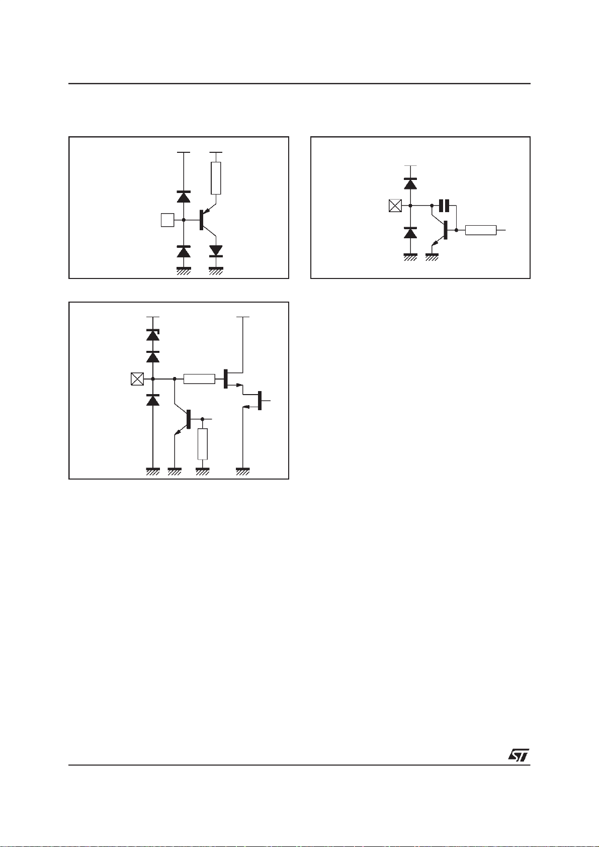
II.4 - Output Section
The H-drive signal is sent to the output through a
shapingstagewhich also controlsthe H-driveduty
cycle (I
secure the scanning power part operation, the
output is inhibitedin the followingcases:
- when V
- when the XRAYprotection is activated,
- during the Horizontalflyback,
- when the HDrive I
The output stage consists of a NPN bipolar
tran s is t or. O n l y th e collect or is accessib le
(see Figure 13).
Figure13
This output stage is intended for ”reverse” base
control, where setting the output NPN in off-state
will control the power scanning transistor in offstate(see ApplicationDiagram).
Figure14 : SafetyFunctions BlockDiagram
2
C adjustable) (see Figure 11). In order to
or VDDare too low,
CC
2
C bit control is off.
V
CC
H-DRIVE26
The maximum output current is 30mA, and the
correspondingvoltage drop of theoutput V
0.4VMax.
Obviouslythe powerscanningtransistorcannotbe
directlydrivenbytheintegratedcircuit.Aninterface
hasto beadded betweenthe circuitand the power
transistoreitherof bipolaror MOS type.
II.5 - X-RAYProtection
TheX-Ray protectionis activatedby applicationof
a high level on the X-Ray input (8V on Pin 25).
It inhibits the H-Drive and B+ outputs.
Thisprotection islatched; it maybe reset either by
switch off or byI2C (seeFigure 14).
V
CC
II.6 - Horizontaland VerticalDynamic Focus
The TDA9109/N delivers a horizontal parabola
whichis addedon a verticalparabolawaveform on
Pin 10. This horizontal parabola comes from a
sawtooth in phase with flyback pulse middle.This
sawtoothis present on Pin 9 where the horizontal
focuscapacitorshouldbethesameas C0to obtain
the correct amplitude (from 2 to 4.7V typically).
2
Symmetry and amplitude are I
9109N-33.EPS
C adjustable
(see Figure 15). The vertical dynamic focus is
trackedwithVPOSand VAMP.Its amplitudecan be
adjusted.Itis alsoaffectedby S andC corrections.
This positive signal once amplified is to be sent to
the CRT focusing grids.
CEsat
is
20/32
V
VSCinh
XRAYProtection
XRAY
VCCoffor I2CReset
HorizontalFlyback
0.7V
VCCChecking
CC
S
Q
R
I2C Drive on/off
HORIZONTAL
OUTPUT
INHIBITION
I2C Rampon/off
VERTICAL
OUTPUT
INHIBITION
BOUT
9109N-34.EPS

OPERATING DESCRIPTION (continued)
Figure15
Horizontal Flyback
Internal Trigged
Horizontal Flyback
Horizontal Focus
Cap Sawtooth
Horizontal Dynamic
Focus Parabola
Output
III - VERTICALPART
III.1- Function
Whenthe synchronizationpulse isnot present, an
internal current source sets the free running frequency.For an external capacitor,C
OSC
= 150nF,
the typical free running frequencyis 100Hz.
The typical free running frequency can be calcu-
lated by :
1
(Hz)=
f
0
1.5⋅10
−5
⋅
C
OSC
A negative or positive TTL level pulse applied on
Pin2 (VSYNC)as wellasa TTLcompositesyncon
Pin 1 can synchronize the ramp in the range
[fmin,fmax].Thisfrequencyrange dependson the
external capacitor con nected on Pin 22.
A 150nF (±5%) capacitor is recommended for
50Hzto 165Hzapplications.
The typical maximum and minimum frequency,at
o
C and without any correction (S correction or
25
C correction),can be calculatedby :
f
= 2.5 x f0and f
(Max.)
(Min.)
= 0.33 x f
0
If S or C corrections are applied, these values are
slightyaffected.
If a synchronization pulse is applied, the internal
oscillator is synchonized immediately but its amplitude changes. An internal correction then adjusts it in less thanhalf a second.The top valueof
theramp(Pin22)is sampledonthe AGC capacitor
(Pin 20) at each clock pulse and a transconductance amplifier modifies thecharge current of the
capacitor in such a way to make the amplitude
again constant.
ThereadstatusregisterprovidestheverticalLockUnlockand the vertical sync polarity information.
Werecommend the use of an AGC capacitor with
low leakage current. A value lower than 100nA is
mandatory.
TDA9109/N
4.7V
400ns
A good stability of the internal closed loop is
reached by a 470nF ± 5% capacitor value on
Pin 20 (VAGC).
2
III.2 - I
C ControlAdjustments
S and C correction shapes can then be added
to this ramp. These frequency independent S
and C corrections are generated internally.
Their amplitudes are adjustable by theirrespec-
2
C registers. They can also be inhibited by
tive I
their select bits.
Finally, the amplitude of this S and C corrected
ramp can be adjusted by the vertical ramp amplitude control register.
The adjustedramp is availableon Pin23 (V
drive an external powerstage.
The gain of this stage can be adjusted (±25%)
depending on its register value.
The mean value of this ramp is driven by its own
2
C register (vertical position). Its value is
I
VPOS = 7/16 ⋅ V
REF-V
Usually VOUTis sent through a resistive divider to
the inverting input of the booster. Since VPOS
derives from V
, the bias voltage sent to the
REF-V
non-invertinginput of the boostershould also derive from V
tooptimize theaccuracy (see Ap-
REF-V
plication Diagram).
III.3 - VerticalMoiré
By using the vertical moiré, VPOS can be modulatedfromframeto frame.Thisfunctionis intended
to cancelthe fringeswhich appearwhen lineto line
intervalis veryclose to the CRTvertical pitch.
The amplitude of the modulation is controlled by
register VMOIRE on sub-address 0C and can be
switched-offvia the control bit D7.
2V
2V
± 300mV.
OUT
)to
9109N-35.EPS
21/32

TDA9109/N
OPERATING DESCRIPTION (continued)
Figure16 : AGCLoop Block Diagram
TRANSCONDUCTANCE
AMPLIFIERCHARGE CURRENT
REF
DISCH.
VSYNCIN
2
SYNCHRO OSCILLATOR
POLARITY
III.4- Basic Equations
Infirstapproximation,the amplitudeoftheramp on
Pin23 (VOUT)is :
V
OUT
-VPOS = (V
OSC-VDCMID
)⋅(1 + 0.25(V
AMP
with:
-V
DCMID
= 7/16 ⋅ V
(middle value of the ramp
REF
on Pin22, typically 3.5V)
-V
OSC=V22
-V
AMP
(rampwith fixed amplitude)
= -1for minimumvertical amplitude register
value and +1 formaximum
- VPOSis calculatedby :VPOS= V
DCMID
+ 0.3V
with VPequals -1 for minimum vertical position
registervalue and+1 for maximum
Thecurrent available on Pin 22 is :
OSC
3
=
⋅ V
⋅ C
REF
8
OSC
⋅ f
with: C
I
: capacitorconnected on Pin 22 and
OSC
f : synchronizationfrequency.
III.5- GeometricCorrections
Theprinciple is representedin Figure17.
Startingfromthe verticalramp, a parabola-shaped
currentis generatedforE/Wcorrection(alsoknown
as Pin Cushion correction), dynamic horizontal
22
OSC
CAP
Vlow
SUB0C/5bits
VPOSITION
SUB06/7bits
VMOIRE
Sawth.
Disch.
VERT_AMP
SUB05/7bits
SAMPLING
20
SAMPLING
CAPACITANCE
S CORRECTION
VS_AMP
SUB07/6bits
COR_C
SUB08/6bits
C CORRECTION
phase controlcorrection, and vertical dynamic Focus correction.
The parabola generator is made by an analog
))
multiplier, the outputcurrent of which is equal to :
DI = k⋅(V
OUT-VDCMID
)
where VOUT is the vertical output ramp (typicallybetween 2 and 5V) and V
REF-V
=8V).
V
DCMID
The VOUT sawtooth is typically centeredon 3.5V.
By changing the vertical position, the sawtooth
P
shiftsby±0.3V.
Inordertohave good screengeometryforanyend
useradjustment, the TDA9109/N hasthe ”geometry tracking” feature, which allows generation of a
dissymetric parabola depending on the vertical
position.
Due to thelarge output stage voltage range (E/W,
Keystone), the combination of tracking function
with maximum vertical amplitude, maximum or
minimum vertical position and maximum gain on
the DAC control may lead to the output stage
saturation. This must be avoided by limiting the
outputvoltagewithapropriateI2Cregistersvalues.
18 BREATH
23
VOUT
2
is 3.5V (for
9109N-36.EPS
22/32

OPERATING DESCRIPTION (continued)
FortheE/Wpart and thedynamichorizontal phase
controlpart, a sawtooth-shapeddifferentialcurrent
in the following form is generated:
DI’= k’ ⋅ (V
OUT-VDCMID
)
Then ∆I and ∆I’ are added and converted into
voltagefor the E/W part.
Each of the two E/W components or the two dynamichorizontalphase control onesmay be inhibitedby theirown I
2
C selectbit.
The E/W parabola is available on Pin 24 via an
Figure17 : GeometricCorrections Principle
2
(3.5V)
V
DCMID
23
Vertical Ramp VOUT
Parabola
Generator
V
(3.5V)
emitter follower output stage which has to be biased by an external resistor (10kΩto ground).
Sincestable in temperature,the device can be DC
coupledwith an external circuitry.
The vertical dynamic focus is combined with the
horizontalfocus on Pin 10.
The dynamichorizontal phase control drivesinternally the H-position, moving the HFLYposition on
the horizontalsawtooth in the range of ± 1.4% T
both for side pin balance and parallelogram.
HORIZONTAL
V.Focus
Amp
EW Amp
DCMID
Keystone
DYNAMICFOCUS
10
24
EW Output
TDA9109/N
H
DynamicFocus
III.6- E/W
EWOUT= 2.5V + K1 (V
OUT-VDCMID
K1is adjustableby thekeystoneI2C register
K2is adjustableby theE/W amplitude I
III.7- DynamicHorizontalPhase Control
I
OUT
=K3(V
OUT-VDCMID
) + K4 (V
K3is adjustableby theparallelogramI2C register
K4is adjustableby theside pin balance I
) + K2 (V
2
C register
OUT-VDCMID
2
C register
OUT-VDCMID
2
)
V
DCMID
(3.5V)
Sidepin Amp
Parallelogram
2
)
To Horizontal
Phase
Sidepin Balance
OutputCurrent
9109N-37.EPS
23/32

TDA9109/N
OPERATING DESCRIPTION (continued)
IV- DC/DC CONVERTER PART
This unit controls the switch-mode DC/DC converter. It converts a DC constant voltage into the
B+ voltage (roughly proportional to the horizontal
frequency)necessary for thehorizontal scanning.
This DC/DC converter can be configuredeither in
step-uporstep-down mode. In bothcases it operates very similarly to the well known UC3842.
IV.1- Step-upMode
OperatingDescription
- ThepowerMOS isswitched-onduringtheflyback
(at the beginning of the positive slope of the
horizontal focus sawtooth).
- The power MOS is switched-offwhen its current
reachesa predeterminedvalue.Forthispurpose,
a sense resistor is inserted in its source. The
voltage on this resistoris sentto Pin16(I
- The feedback(com i ngeitherfrom the EHV or from
theflyback )is dividedtoa voltage clo s eto 4.8Vand
compar edto theinter nal4.8Vrefer ence(I
VREF
differenceisamplif i edby anerroramplifi er,theoutput
ofwhichcontrolsthepowerMOSswitch-offcurrent.
MainFeatures
- Switching synchronized on the horizontal frequency,
- B+ voltage always higher than the DC source,
- Currentlimited on a pulse-by-pulsebasis.
IV.2- Step-down Mode
In step-down mode, the Isense information is not
usedanymoreandthereforenot sentto the Pin16.
This mode is selected by connectingthis Pin16 to
a DC voltage higher than6V (for example V
Figure18 : DC/DCConverter
I2C
DAC
7bits
8V
4.8V ±20%
22kΩ
± I
adjust
95dB
1MΩ
A
Horizontal Dynamic
Focus Sawtooth
Σ
1.2V
COMPREGIN
L
+
1.2V
I
1/3
SENSE
161415
SENSE
).The
REF-V
C1
C2
C3
8V
).
OperatingDescription
- The powerMOSis switched-onas forthestep-up
mode.
- The feedbackto theerroramplifier is done as for
the step-up mode.
- T he power MOS is switched-off whe n the
HFOCUSCAP voltage get higher than the error
amplifier output voltage.
Main Features
- Switching synchronized on the horizontal frequency,
- B+ voltage always lower than the DC source,
- No currentlimitation.
IV.3- Step-up and Step-downModeComparison
In step-down mode the control signal is inverted
compared with the step-upmode.
The reason for this is the following:
- In step-upmode, the switch is a N-channelMOS
referencedto ground and made conductive by a
high level on its gate.
- In step-down,a high-side switch is necessary.It
can be either a P-or a N-channel MOS.
- ForaP-channelMOS,thegateiscontr olleddire ctly
fromPin28throughacapacitor(thisallow stospare
aTransformer).Inthiscase,anegative-goingpulse
isneededtomaketheMOSconductive.Therefore
itis necessar yto inver tthecontrolsignal.
- For a N-channelMOS,a transformeris needed
to control the gate. The polarity of the transformer can be easily adapted to the negative-
).
6V
goingcontrol pulse.
HDF Disc
400ns
down
S
Q
R
up
Inhibit SMPS
C4
Command step-up/down
down
up
TDA9109/N
BOUT
12V
28
24/32
V
B+
9109N-38.EPS

INTERNAL SCHEMATICS
Figure19
TDA9109/N
Figure20
Pins 1 -2
H/HVIN
VSYNCIN
Figure21
PLL2C
5V
5V
Ω
200
20k
Ω
9109N-39.EPS
3
HLOCKOUT
9109N-40.EPS
Figure22
12V
HREF
13
4
C0
12V
5
HREF
13
Figure23
R0
HREF HREF
13 13
12V
6
9109N-41.EPS
Figure24
9109N-43.EPS
9109N-42.EPS
7PLL1F
9109N-44.EPS
25/32

TDA9109/N
INTERNAL SCHEMATICS (continued)
Figure25
Figure26
HPOSITION
Figure27
HREF
12V
12V
9109N-45.EPS
HFOCUS
CAP
9
8
HREF
13
9109N-46.EPS
Figure28
12V
12V
10HFOCUS
HFLY
12V
12
HREF
13
Figure29
COMP
14
26/32
9109N-47.EPS
Figure30
9109N-49.EPS
9109N-48.EPS
12V
15REGIN
9109N-50.EPS

INTERNAL SCHEMATICS (continued)
Figure31
TDA9109/N
Figure32
16
I
SENSE
Figure33
VAGCCAP
12V
20
12V
9109N-51.EPS
Figure 34
12V
18BREATH
9109N-52.EPS
12V
22VCAP
Figure35
23
VOUT
12V
9109N-53.EPS
Figure36
9109N-55.EPS
9109N-54.EPS
12V
24EWOUT
9109N-56.EPS
27/32
TDA9109/N
INTERNAL SCHEMATICS (continued)
Figure37
12V
25
XRAY
Figure 38
12V
HOUT-BOUT
Pins 26-28
Figure39
Pins 30-31
SDA - SCL
12V
9109N-57.EPS
9109N-59.EPS
9109N-58.EPS
28/32

APPLICATION DIAGRAMS
Figure40 : DemonstrationBoard
+12V
CC2
10µF
CC3
47pF
CC1
100nF
TB1
TB2
CC
CDA
TA2
TA1V
12345678
CC4
47pF
+12V
PC2
47kΩ
R35
+12V
10kΩ
C22
33pF
J8
HFLY
J9
DYN
FOCUS
J19
1
2
3
4
CON4
REGIN
I
SENSE
GND
B+OUT
R75
10kΩTP8
EHT
COMP
PC1
47kΩ
+12V
CDBIBIBQBQB
QA
IA
IA
R10
10kΩ
R8
10kΩ
R25
1kΩ
R24
10kΩ
R73
1MΩ
R76
47kΩ
QA
C25
33pF
10kΩ
910111216 15 14 13
GND
HOUT
L4
47µH
C16
()
*
C27
47µF
JP1
R51
82kΩ
1kΩ
R74
10kΩ
P1
R77
15kΩ
TP17
ICC1
MC14528
C51
100nF
R57
+12V
TP13
J12
6.49kΩ 1%
C33
100nF
R50
1MΩ
C60
100nF
J11
TP16
TP10
C7 22nF
820pF 5%
R23
C13 10nF
R36 1.8kΩC31 4.7µF
C17 1µF
820pF 5%
HREF
TP1
C28
C34
C46
1nF
C47
100pF
IC4
TDA9109/N
1
H/HVIN
VSYNCIN
2
HLOCKOUT SCL
3
PLL2C
4
C0 B+OUT
5
R0 GGND
6
PLL1F HOUTCOL
7
HPOSITION XRAYIN
8
HFOCUSC EWOUT
9
FOCUS VOUT
10
HGND VCAP
11
HFLY VREF
12
HREF VAGCCAP
13
COMP VGND
14
REGIN BREATH
15
I
16
SENSE
R58
10Ω
SDA
BGND
TDA9109/N
J16 J15
+5V
+5V
L1
R39
22µH
C30
C6
C12
150nF
C15
470nF
HOUT
C49
100nF
TP14
R53
1kΩ
BC557
BC547
+12V
100nF
Q4
Q5
C2
4.7kΩ
C32
100nF
C5
100µF
C48
10µF
R7 10kΩ
R45 33kΩ
R52
3.9kΩ
C50
10µF
+12V
C3
47µF
22µH
L3
+5V
32
100µF
31
30
29
CC
100nF
28
27
26
25
24
23
22
21
20
19
18
17
J14
432
1
C39
22pF
R29
R42
4.7kΩ
100Ω
C40
22pF
R41
100Ω
SCL
SDA
+12VV
R56
560Ω
D2
1N4148
100nF
R2
5.6kΩ
IC1
R40
36kΩ
TDA8172
R1
12kΩ
C41
470pF
VERTICAL DEFLECTION STAGE
C45
R49
10µF
R17
VSYNC
+5V
TP6
TP7
5.6kΩ
FBLK
R18
39kΩ
R5
242322212019181716151413
PWM6
PWM7
PWM0
PWM1
123456789101112
R30
10kΩ
E/W POWER STAGE
R31
27kΩ
R19
270kΩ
C11 220pF
R11
220Ω
0.5W
R4
1Ω
0.5W
PWM5
SCL
SDA
RST
GNDRGBTEST
XTALOUT
XTALIN
PWM2
PWM3PWM4
X1
8MHz
C38
33pF
+12V
C36
1µF
R37
27kΩ
R34
1kΩ
R9
470Ω
D1
1n4001
C4
2
6
7
3
1
4
C10
470µF
-12V
HSYNC
CKOUT
PXCK
V
DD
22µH
C43
C37
33pF
47µF
R15
1kΩ
270kΩ
Q1
BC557Q2BC557
R33
4.7kΩ
C14
470µFC9100nF
C10
100µF
35V
5
220nFR31.5Ω
C8
100nF
L2
C1
IC3 - STV9422
R43
10kΩ
C42
1µF
R38
2.2Ω
Q3
TIP122
+12V
-12V
TP4 TP3
V YOKE
22kΩ
+5V
TILT
J13
J1
3W
E/W
J2
J3
J6
1
2
3
J18
J17
HOUT
()*Optional
9109N-60.EPS
29/32

TDA9109/N
APPLICATION DIAGRAMS (continued)
Figure41 : PCBLayout
30/32
9109N-61.EPS

APPLICATION DIAGRAMS (continued)
Figure42 : ComponentsLayout
TDA9109/N
31/32
9109N-62.EPS

TDA9109/N
PACKAGE MECHANICAL DATA
32 PINS - PLASTICSHRINK DIP
Dimensions
Min. Typ. Max. Min. Typ. Max.
Millimeters Inches
A 3.556 3.759 5.080 0.140 0.148 0.200
A1 0.508 0.020
A2 3.048 3.556 4.572 0.120 0.140 0.180
B 0.356 0.457 0.584 0.014 0.018 0.023
B1 0.762 1.016 1.397 0.030 0.040 0.055
C 0.203 0.254 0.356 0.008 0.010 0.014
D 27.43 27.94 28.45 1.080 1.100 1.120
E 9.906 10.41 11.05 0.390 0.410 0.435
E1 7.620 8.890 9.398 0.300 0.350 0.370
e 1.778 0.070
eA 10.16 0.400
eB 12.70 0.500
L 2.540 3.048 3.810 0.100 0.120 0.150
Information furnished is believed to be accurate and reliable. However, STMicroelectronics assumes no responsibility for the
consequences of use of such information nor for any infringement of patents or other rights of third parties which may result from
its use. No licence is granted by implication or otherwise under any patent or patent rights of STMicroelectronics. Specifications
mentioned in this publication are subject to change without notice. This publication supersedes and replaces all information
previouslysupplied.STMicroelectronicsproducts are notauthorized foruse ascriticalcomp onentsin lifesupportdevicesor systems
without express written approval of STMicroelectronics.
Purchase of I
Rights to use these components in a I
Australia - Brazil - Canada - China - France - Germany - Italy- Japan - Korea - Malaysia - Malta - Morocco- The Netherlands
2
C Components of STMicroelectronics, conveys a license under the Philips I2C Patent.
Singapore - Spain - Sweden - Switzerland- Taiwan- Thailand - United Kingdom - U.S.A.
The ST logo is a trademark of STMicroelectronics
1998 STMicroelectronics - All Rights Reserved
2
2
the I
C Standard Specifications as defined by Philips.
STMicroelectronics GROUP OF COMPANIES
C system,is granted provided that the system conforms to
PMSDIP32.EPS
SDIP32.TBL
32/32
 Loading...