Philips TDA8980 Datasheet

Complete ATSC (VSB)/NTSC channel
decoding solution with just two ICs
This chipset combines Philips’ long experience in analog TV with our
innovative approach to DTV, creating an outstanding system solution
showcasing Philips’ mixed signal technology expertise and offering very
high levels of integration, performance and flexibility. Designed for
analog and digital TV systems in North America and other ATSC
countries, the chipset enables manufacturers to design systems offering
end-users significantly improved reception at an attractive price.
The two key chips featured are the TDA8980 TV input processor and
the TDA8961 8-VSB demodulator/decoder for the ATSC DTV
standard. Designed specifically to reduce the chip count of first
generation front-ends, the TDA8980 eliminates many components by
integrating NTSC decoding, an IF circuit, picture and sound
demodulation and VSB downconversion, all into a single device.
This chipset gives true design flexibility, with the TDA8980 offering
both analog and digital capability, with comprehensive analog source
selection and also providing format conversion. This ensures glueless
support for the many legacy inputs a digital hybrid receiver is likely to
require.
Benefiting from real-world experience of VSB reception, Philips’ second
generation VSB demodulator handles the many problems caused by
man-made and naturally occurring echoes. Intelligent techniques in the
decoder allow it to cope with the delays and reflections caused by indoor
environments full of objects and moving people. Its maximum equalizer
length of 80 µs in conjunction with external software allows the receiver
to cope with very long static echoes. Patented NTSC co-channel
interference technology prevents strong NTSC signals from interfering
with their less powerful DTV counterparts on the same channel, without
the noise penalty associated with regular comb filter schemes.
As the roll out of digital TV accelerates, DTV receiver
manufacturers are looking for improved performance, flexibility
and cost reductions to meet the demands of the consumer
market. Philips’ latest reference design meets these stringent
requirements, using two new ICs, the second generation
TDA8961 VSB demodulator and the TDA8980 integrated
ATSC/NTSC TV input processor
Applications
• Digital ATSC/NTSC-compliant TV receivers and
Set T op Converters
• DTV-equipped PC/multimedia applications
Tightly integrated, flexible DTV front-end
• Second generation ATSC/NTSC channel decoding
chipset
• Greatly reduced chip count due to single-chip
ATSC/NTSC TV input processor providing
NTSC TV decoding and VSB IF downconversion
• Analog source selection and format conversion
High performance reception
• Urban reception improvement
• Unique co-channel filter to reduce interference
from strong NTSC signals
• Ability to handle very long static echoes (up to 80 µs) in
conjunction with external software
ATSC/NTSC digital TV
front-end chipset
Second generation chipset

TDA8980HL ATSC/NTSC TV
INPUT PROCESSOR
Key features
• NTSC-M colour decoder tuned with a
12 MHz reference crystal
(or external clock signal)
• VSB IF circuit for pre-processing
DTV signals
• Alignment-free PLL demodulator Vision
IF circuit without external components
• Sound IF amplifier with separate input
for single reference QSS mode and
separate AGC circuit
• Alignment-free FM sound demodulator
generates the input signal for a BTSC
stereo decoder
• Video source selection with 2 external
CVBS or Y/C inputs and an
independently switchable output
• Two 10-bit video ADCs for converting
selected YUV signals (video mode)
or downconverted I&Q signals
(VSB mode)
• Two 16-bit audio A/D converters and
I
2
S formatter
• Up to four stereo analog inputs and
one I2S input
• ITU656 or VSB formatter
• Direct input to video ADCs
Integrating many components into a single
chip, the TDA8980HL is designed for both
TV and multimedia applications. Containing
an NTSC-M colour decoder, an IF circuit
and ADCs for audio and video, it can also
generate a ‘mixed down’ I signal for
demodulation of a digital broadcast VSB
input. An I
2
C-bus controlled internal switch
enables the device to switch between analog
NTSC and digital 8-VSB IF signals.
When decoding NTSC, the chip digitizes the audio signals into an
I
2
S stream using on-chip audio stereo 16-bit ADCs, and the video
information into an ITU656 stream via the on-chip video ADCs.
An incoming 6 MHz wide 8-VSB IF signal is downconverted to a low
IF, centred at 4 MHz, which is digitized using an on-chip 10-bit ADC
and gluelessly interfaced to the VSB demodulator for further
processing. In a typical application, the TDA8980 handles AGC,
eliminating the need for external components such as an op-amp loop
integrator.
It has an internal 2-D adaptive comb filter for NTSC, and a YUV
interface allows simple connection of additional picture enhancement
ICs such as a 3-D comb filter. For sound decoding, external
devices - a BTSC sounder decoder, for example - can be connected.
TDA8961 DTV DEMODULATOR/DECODER
General features
• One-chip ATSC-compliant demodulator and concatenated
Trellis (Viterbi)/Reed-Solomon decoder with de-interleaver
and de-randomizer
• Parallel (8-bit) or serial MPEG2 transport stream output
• On-board I2C-bus interface
• MPEG2 serial transport stream input
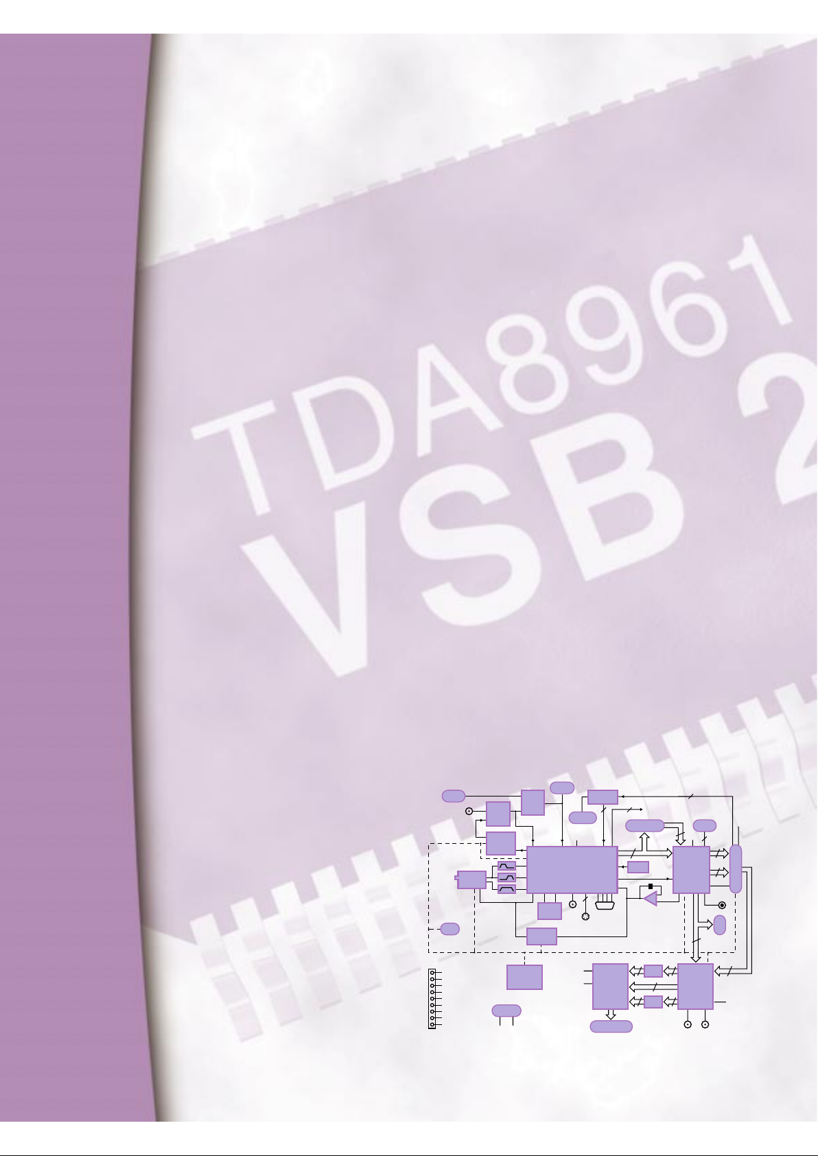
COMPLETE REFERENCE DESIGN FOR
HYBRID ATSC/NTSC RECEIVER FRONT-ENDS
This reference design demonstrates a complete solution for building hybrid ATSC/NTSC receiver front-ends for
HDTV sets, STBs and PC/multimedia applications, using just two highly integrated, second generation ICs.
11
MSD051
9
11
9
4
3
3
2
5
12
30
6
8
8
reset
reset
serial TS
output
diag
serial TS
input
9
TS in
I2C
EEPROM &
CONTROL
SAA7146
PCI connector
FPGA
Errror
+5 V +12 V
V
CC
TDA8961
(w/socket)
TDA8980
(w/socket)
TS
TS + diag +
control +
status
6
status
FIFO
12 MHz
AUDIO
MUX
stereo
audio in
4.5 MHz
TRAP
TUNER
tuner
AGC
12 MHz
FIFO
power
MPOC output
S/PDIF in
JTAG
IF AGC
CD in
CD out
I
2
C
I
2
C
I2S out
5 V
I
2
C
3 V
I
2
C
TS connector
diag
RGBS/YUVS
in
InRange_1
Tuner_Lock
FE_Lock
EQ_Lock
FSHNDSHK
FPGA_1
FPGA_2
FPGA_3
comp.
video
in
S-video
in
reset
AUDIO
MIX
PCF9851
I
2
C ADC
TDA9851
BTSC
DECODER
TDA1315
V
CC
I
2
S
out
I
2
S out
I
2
S in
L3
bus
parallel
output
 Loading...