

Philips TDA8961 Datasheet
INTEGRATED CIRCUITS
DATA SH EET
TDA8961
ATSC Digital Terrestrial TV
demodulator/decoder
Objective specification
File under Integrated Circuits, IC02
2000 May 19

Philips Semiconductors Objective specification
ATSC Digital Terrestrial TV
demodulator/decoder
FEATURES
General features
• One-chip ATSC-compliant demodulator and
concatenated trellis (Viterbi)/Reed Solomon decoder
with de-interleaver and de-randomizer
• 0.35 µm process
• 3.3 V device
• QFP80 package
• Boundary Scan Test (BST)
• 12 MHz external clock
• 36 MHz output for external D/A converter
• Parallel or serial MPEG-2 transport stream output.
8-Vestigial Side Band (VSB) demodulator
• Accepts 10-bit IF data sampled at 36 MHz
• 6 MHz wide IF signal, centered at 4 MHz
• On-chip digital circuitry for tuner AGC
• Square-root raised-cosine filterwith 11.5% roll-off factor
• Fully internal carrier recovery loop
• No need for external voltage controlled crystal oscillator
due to internal sample rate converter
• Fully internal symbol timing recovery with
programmable loop filters
• Technology to handle dynamic multipath conditions.
Adaptive equalizer
• Including feed forward and feedback sections with
Decision Feedback Equalizer (DFE) structure
• Rangeof −2.3 to +22.5 µs by default(inconjunction with
external software, −2.3 to +80 µs)
• Adaptation based on ATSC field sync (trained) and/or
8-VSB data (blind).
NTSC co-channel interference filter
Patented NTSC co-channel interference technology with
low noise penalty.
TDA8961
On-chip forward error correction
• Trellis (Viterbi) decoder
• Rate2⁄3 (Rate1⁄2 Ungerboeck code based)
• (207, 187, T = 10) Reed Solomon code
• Internal convolutional de-interleaving (I = 52; using
internal memory)
• External indication of uncorrectable error;
transport_error_indicator bit in MPEG packet header is
also set
• De-randomizer based on ATSC standard
• Segment error rate readable through I2C.
2
C interface
I
I2C-bus interface to initialize and monitor the demodulator
and Forward Error Correction (FEC) decoder. An
operation without I2C-bus is possible (default).
System interfaces
• 8-bit wide or serial MPEG-2 transport stream interface
• ITU656 bypass mode
• MPEG-2serial transport stream input to reduceexternal
components when the IC is combined in asystem with a
Quadrature Amplitude Modulation (QAM), Quadrature
Phase Shift Keying (QPSK) or Orthogonal Frequency
Division Multiplexing (OFDM) channel decoder.
APPLICATIONS
• Digital ATSC compliant TV receiver
• Personal computers with digital television capabilities
• Set top-boxes.
ORDERING INFORMATION
PACKAGE
TYPE NUMBER
NAME DESCRIPTION VERSION
TDA8961 QFP80 plastic quad flat package; 80 leads (lead length 1.95 mm);
body14 × 20 × 2.8 mm
2000 May 19 2
SOT318-2
Philips Semiconductors Objective specification
ATSC Digital Terrestrial TV
demodulator/decoder
GENERAL DESCRIPTION
The TDA8961 is an Advanced Television Systems
Committee (ATSC)-compliant demodulator and FEC
decoder for reception of 8-VSB modulated signals for
terrestrial and cable applications:
• Terrestrial: reception of 8-VSB modulated signals via
standard 6 MHz VHF/UHF terrestrial TV channels (TV
channels 2 to 69 in the United States).
• Cable: reception of 8-VSB modulated signals via
standard 6 MHz VHF/UHF cable TV channels.
An application using the TDA8961 and the TDA8980
NTSC/ATSC TV input processor for TV and Multi-Media is
shown in Fig.1. A tuner converts the incoming RF signal to
a fixed IF centered at 44 MHz. The output signal from the
tunerisfilteredandfedtotheTDA8980whichperformsthe
following functions:
• Decodes the analog NTSC signals: The audio signals
aredigitized,using on-chip audio stereo A/D converters,
intoanI2S-busstream;thevideoinformationisdigitized,
using on-chip video A/D converters, into an ITU656
stream.
TDA8961
• Down converts the incoming 6 MHz wide 8-VSB IF
signal to a low-IF signal centered at 4 MHz: The low-IF
signal is then digitized, using an on-chip 10-bit A/D
converter, and fed to the TDA8961 for further
processing. In this application, AGC is also managed by
the TDA8980 so that no other external components,
such as an operational amplifier loop integrator, are
required.
Although the TDA8980 has an internal 2-D comb filter,
external filters such as a 3-D comb filter and other picture
improvementdevices can easily be connected. Soundcan
be decoded using an external device such as the
TDA9851 I2C-bus controlled economic BTSC stereo
decoder. This IC has an internal switch allowing it to
process either analog NTSC IF or digital 8-VSB IF signals.
A12 MHzclocksignal is generated using a 12 MHz crystal
connected to the TDA8980. The TDA8961 also uses this
clocksignal which is fed from theTDA8980to pin XTALI of
the TDA8961.
handbook, full pagewidth
TUNER
2
I
C
NTSC
SAW
FILTER
FLAT
SAW
FILTER
TDA8980
TVIFIN
VSBIFIN
TUNERAGC
2
I
C
X12MOUT
D9 to D0
REF12M
12 MHz
VCLK
VIFAGC
X12MIN
I2C
master
ADCLK
ADIN9 to ADIN0
XTALI
AGCOUT
2
PDI0 PDISYNC PDIVAL
I
C
TDA8961
PDOVAL
PDOERR
PDO7 to PDO0
PDOSYNC
PDOCLK
PDICLK PDIERR
serial MPEG-2 transport
stream input
Fig.1 Front-end design for a hybrid TV system using the TDA8980 and TDA8961.
MPEG-2
transport
stream
MGU085
2000 May 19 3
Philips Semiconductors Objective specification
ATSC Digital Terrestrial TV
demodulator/decoder
The incoming data has a sample rate of 36 MHz. This is
internally converted to a sample rate of 21.52 MHz which
is twice the 8-VSB symbol rate. This patented Philips
Semiconductors’ technology eliminates the need for
external symbol timing recovery loop components. When
theTDA8980 is decoding analog NTSC,the TDA8961 can
be set to a ITU656 bypass mode which allows the 8-bit
ITU656 data output from the TDA8980 to appear at the
TDA8961 Moving Pictures Expert Group (MPEG-2)
transport stream output, from where it can be fed to the
main graphics display device in the system.
The recovery of the carrier is performed entirely within the
TDA8961. This function consists of a digital frequency and
Frequency Phase-Locked Loop (FPLL).
Data shaping is performed by a square-root raised-cosine
(half Nyquist) filter having a roll-off factor of 11.5%.
After the TDA8961 has performed carrier recovery,
Nyquist filtering and symbol timing recovery, it then
performs adaptive equalization. The adaptive equalizer
usesaDFEstructurewithequalizationbasedontheATSC
field sync (trained equalization) and/or the 8-VSB data
itself (blind equalization).
The equalizer is followed by a patented NTSC co-channel
interference filter which removes any unwanted NTSC
signal interference from the 8-VSB terrestrial DTV signal.
After trellis decoding, the stream is de-interleaved to a
depth of 52 by a convolutional de-interleaver whose
memory is provided on-chip. The Reed Solomon decoder
is ATSC-compliant, with a length of 207, and able to
TDA8961
correct up to 10 bytes. The decoded stream is then
de-randomized using a pseudo-random binary sequence
(PRBS) and the data passed to a FIFO which prevents the
appearance of irregular gaps in the output data.
The output of the TDA8961 is a clock signal and an
ATSC-compliant MPEG-2 packetized data stream. Signal
flag outputs are provided to indicate the occurrence of
sync bytes, valid data bytes and uncorrected Reed
Solomon blocks. The packetized data stream is available
in either an 8-bit parallel, or a 1-bit serial format for
connection to an MPEG-2 transport stream demultiplexer.
An application using the TDA8961 and a stand-alone
TDA9829 Downconverter for DVB (Digital Video
Broadcast)withanA/DconverterisshowninFig.2.Atuner
converts the incoming RF signal to a fixed IF centered at
44 MHz. The output signal from the tuner is filtered using
two Surface Acoustical Wave (SAW) filters and then down
converted to an IF of 4 MHz by the TDA9829. The signal
is then digitized by an A/D converter at a sample rate of
36 MHz using the clock signal output from the TDA8961.
The full input range of the A/D converter is utilized by
placing it within what is effectively a fine-AGC loop
integrator circuit which has a variable gain stage at the
output of the IF downmixer section. However, it is also
possible to apply the AGC control output of the TDA8961
to the tuner via the integrator. The peak level of the input
signals to the TDA8961 is determined by the AGC output
detector which is located just after the A/D.
V
AGC
TDA9829
VCO
96 MHz
integrator
V
oDVB
AGC
V
ref
AGCOUT
A
ADIN9 to
ADIN0
D
ADCLK
CLK36
÷8
PDO7 to
PDO0
TDA8961
XTALI
12 MHz
MPEG-2
transport
stream
MGU086
handbook, full pagewidth
RF
FILTER
TUNER RF
SAW
44 MHz
SAW
FILTER
V
iIF
IF DOWNMIXER
OSCILLATOR
Fig.2 Front-end design for the TDA8961 using a stand-alone IF down converter (TDA9829) and A/D converter.
2000 May 19 4
Philips Semiconductors Objective specification
ATSC Digital Terrestrial TV
TDA8961
demodulator/decoder
QUICK REFERENCE DATA
SYMBOL PARAMETER CONDITIONS MIN. TYP. MAX. UNIT
V
DD
I
DD
f
clk
f
sym
f
s
f
c(IF2)
IL implementation loss −−−dB
α
ro
t
acq
T
amb
P
tot
Note
1. Corresponds to 12 training sequences.
supply voltage 2.7 3.3 3.6 V
supply current VDD= 3.3 V − 390 − mA
clock frequency − 12 − MHz
symbol frequency − 10.76 − Msymbols/s
sample frequency − 36 − MHz
second IF centre frequency − 4 − MHz
half Nyquist filter roll-off factor − 11.5 − %
acquisition time note 1 −−290 ms
ambient temperature −20 − +70 °C
total power dissipation − 1.3 − W
2000 May 19 5
Philips Semiconductors Objective specification
ATSC Digital Terrestrial TV
demodulator/decoder
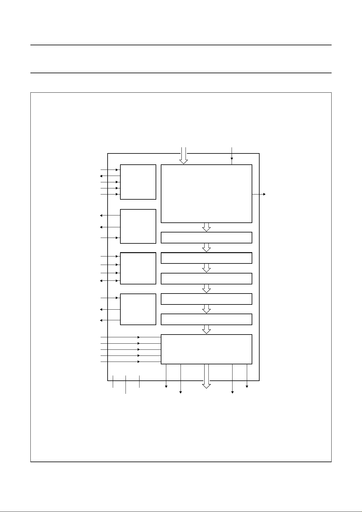
BLOCK DIAGRAM
handbook, full pagewidth
TDI
TCK
20
23
19
22
21
78
79
77
TMS
TDO
TRST
LOCKINDIC
EQLOCKINDIC
RST_AN
BOUNDARY
SCAN TEST
CONTROLLER
CONTROL
ADIN9 TO ADIN0 ADCLK
10, 9, 8, 7, 6,
5, 4, 3, 2, 1
DIGITAL FRONT-END:
SAMPLE RATE CONVERTER
*
FINE AGC
*
CARRIER RECOVERY
*
HALF NYQUIST FILTERING
*
SYNC RECOVERY AND PILOT REMOVAL
*
SYMBOL TIMING RECOVERY
*
ADAPTIVE EQUALIZATION
*
NTSC CO-CHANNEL INTERFACE FILTER
80
TDA8961
66
AGCOUT
A0
A1
SCL
SDA
XT ALI
XT ALO
CLK36
PDISYNC
PDICLK
PDIERR
PDIVAL
PDI0
13
14
15
16
69
70
75
26
30
32
28
27
34
FSYNC
I2C-BUS
INTERFACE
CLOCK
GENERATION
TDA8961
35
FSHNDSHK
SSYNC
67
TRELLIS DECODER
DE-INTERLEAVER
REED SOLOMON DECODER
DE-RANDOMIZER
OUTPUT FORMATTER
39 40
PDOSYNC
PDOV AL PDOERR
PDO7 TO PDO0
43, 44, 45,
47, 48, 49,
51, 52
37 41
PDOCLK
MGU087
Fig.3 Block diagram.
2000 May 19 6
Philips Semiconductors Objective specification
ATSC Digital Terrestrial TV
TDA8961
demodulator/decoder
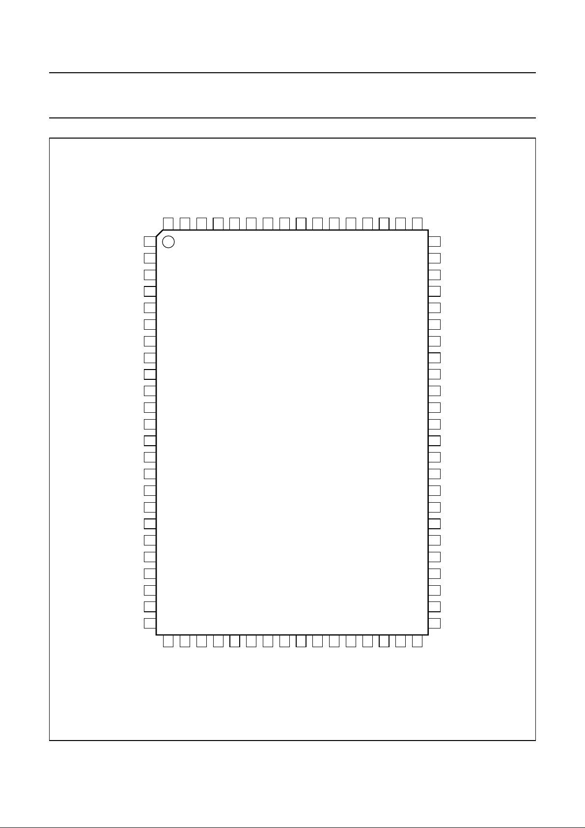
PINNING
SYMBOL PIN I/O DESCRIPTION
ADIN0 1 I data input bit 0 (LSB)
ADIN1 2 I data input bit 1
ADIN2 3 I data input bit 2
ADIN3 4 I data input bit 3
ADIN4 5 I data input bit 4
ADIN5 6 I data input bit 5
ADIN6 7 I data input bit 6
ADIN7 8 I data input bit 7
ADIN8 9 I data input bit 8
ADIN9 10 I data input bit 9 (MSB)
V
DDD1
V
SSD1
A0 13 I I
A1 14 I I
SCL 15 I I
SDA 16 I/O I
V
DDD2
V
SSD2
TDI 19 I TAP controller data input; note 1
TMS 20 I TAP controller test mode select; note 1
TCK 21 I TAP controller test clock; note 1
TRST 22 I TAP controller asynchronous reset (active LOW); notes 1 and 2
TDO 23 O TAP controller test data (3-state); note 1
V
DDD3
V
SSD3
PDISYNC 26 I transport stream interface packet sync indicator
PDI0 27 I transport stream interface packet data bit 0
PDIVAL 28 I transport stream interface packet data valid signal
V
DDD4
PDICLK 30 I transport stream interface packet data clock signal
V
SSD4
PDIERR 32 I transport stream interface packet error signal
V
DDD5
FSYNC 34 I field sync strobe (for debug modes)
SSYNC 35 I segment sync strobe (for debug modes)
V
SSD5
PDOERR 37 O transport stream interface packet error signal (3-state)
V
DDQ1
PDOSYNC 39 O transport stream interface packet sync indicator signal (3-state)
PDOVAL 40 O transport stream interface packet data valid indicator signal (3-state)
11 − digital core supply voltage 1 (3.3 V)
12 − digital core ground 1
2
C-bus slave address bit 0
2
C-bus slave address bit 1
2
C-bus clock
2
C-bus serial data
17 − I/O supply (3.3 V)
18 − digital core ground 2
24 − digital core supply voltage 3 (3.3 V)
25 − digital core ground 3
29 − digital core supply voltage 4 (3.3 V)
31 − digital core ground 4
33 − digital core supply voltage 5 (3.3 V)
36 − digital core ground 5
38 − I/O supply voltage 1 (3.3 V)
2000 May 19 7
Philips Semiconductors Objective specification
ATSC Digital Terrestrial TV
TDA8961
demodulator/decoder
SYMBOL PIN I/O DESCRIPTION
PDOCLK 41 O transport stream interface packet data clock signal (3-state)
V
SSQ1
PDO7 43 O transport stream interface packet data bit 7 (3-state)
PDO6 44 O transport stream interface packet data bit 6 (3-state)
PDO5 45 O transport stream interface packet data bit 5 (3-state)
V
DDQ2
PDO4 47 O transport stream interface packet data bit 4 (3-state)
PDO3 48 O transport stream interface packet data bit 3 (3-state)
PDO2 49 O transport stream interface packet data bit 2 (3-state)
V
SSQ2
PDO1 51 O transport stream interface packet data bit 1(3-state)
PDO0 52 O transport stream interface packet data bit 0 (3-state)
V
DDQ3
n.c. 54 not connected
n.c. 55 not connected
V
SSQ3
n.c. 57 not connected
n.c. 58 not connected
n.c. 59 not connected
V
DDQ4
n.c. 61 not connected
n.c. 62 not connected
n.c. 63 not connected
V
SSQ4
n.c. 65 not connected
AGCOUT 66 O AGC control (3-state)
FSHNDSHK 67 O field sync strobe or symbol capture memory handshake signal
V
DDA1
XTALI 69 I external crystal
XTALO 70 O external crystal
V
SSA1
V
DDA2
n.c. 73 not connected
V
DDQ5
CLK36 75 O 36 MHz clock signal
V
SSQ5
RST_AN 77 I asynchronous reset (active LOW)
LOCKINDIC 78 O front-end lock indicator
EQLOCKINDIC 79 O equalizer lock indicator
ADCLK 80 I incoming data sampling clock signal (36 MHz)
42 − I/O ground 1
46 − I/O supply voltage 2 (3.3 V)
50 − I/O ground 2
53 − I/O supply 3 (3.3 V)
56 − I/O ground 3
60 − I/O supply 4 (3.3 V)
64 − I/O ground 4
68 − analog supply voltage (3.3 V)
71 − analog ground 1
72 − analog supply 2 (3.3 V)
74 − I/O supply 5 (3.3 V)
76 − I/O ground 5
2000 May 19 8

Philips Semiconductors Objective specification
ATSC Digital Terrestrial TV
TDA8961
demodulator/decoder
Notes
1. Input pins TCK, TDI, TMS and TRST have an internal pull-up transistor and must be connected to ground when not
used; pin TDO is a 3-state output in accordance with IEEE 1149.1.
2. Pin TRST is active LOW. It can be used to immediately force the Test Access Port (TAP) controller to the test logic
reset state (normal operation) in accordance with IEEE 1149.1.
2000 May 19 9
Philips Semiconductors Objective specification
ATSC Digital Terrestrial TV
demodulator/decoder
ADCLK
handbook, full pagewidth
ADIN0
ADIN1
ADIN2
ADIN3
ADIN4
ADIN5
ADIN6
ADIN7
ADIN8
ADIN9
V
DDD1
V
SSD1
SDA
V
DDD2
V
SSD2
TMS
TCK
TRST
TDO
V
DDD3
A0
A1
SCL
TDI
1
2
3
4
5
6
7
8
9
10
11
12
13
14
15
16
17
18
19
20
21
22
23
24
EQLOCKINDIC
80
79
25
26
LOCKINDIC
RST_AN
78
77
27
28
SSQ5
V
76
29
CLK36
75
30
DDQ5
V
n.c.
74
73
TDA8961
31
32
DDA2VSSA1
V
72
71
33
34
XTALO
70
35
XTALI
69
36
DDA1
V
68
37
FSHNDSHK
AGCOUT
67
66
38
39
n.c.
65
40
64
63
62
61
60
59
58
57
56
55
54
53
52
51
50
49
48
47
46
45
44
43
42
41
MGU088
TDA8961
V
SSQ4
n.c.
n.c.
n.c.
V
DDQ4
n.c.
n.c.
n.c.
V
SSQ3
n.c.
n.c.
V
DDQ3
PDO0
PDO1
V
SSQ2
PDO2
PDO3
PDO4
V
DDQ2
PDO5
PDO6
PDO7
V
SSQ1
PDOCLK
SSD3
V
PDI0
PDISYNC
V
PDIVAL
DDD4
V
PDICLK
SSD4
PDIERR
Fig.4 Pin configuration.
2000 May 19 10
DDD5
V
FSYNC
SSYNC
SSD5
V
DDQ1
V
PDOERR
PDOVAL
PDOSYNC
Philips Semiconductors Objective specification
ATSC Digital Terrestrial TV
demodulator/decoder
FUNCTIONAL DESCRIPTION
The internal architecture of the TDA8961 basically
comprises two parts:
• The front-end: containing the AGC, carrier recovery,
halfNyquistfilter,symboltimingrecovery,syncrecovery
and adaptive equalization sections.
• The back-end: containing the NTSC co-channel
rejection filter, trellis decoder, de-interleaver, the Reed
Solomon decoder and de-randomizer sections.
Sample rate converter
INTRODUCTION
The sample rate converter section changes the incoming
data frequency of 36 MHz to an internal sampling
frequency of twice the symbol rate.
The 10-bit wide data from either the TDA8980 or a
stand-alone A/D converter (TDA8763A is recommended)
arrives at the sample rate converter input of the TDA8961
via inputs ADIN9 to ADIN0. The format of the incoming
samples can be programmed by the status of I2C-bus
bit AD_FMT (see Table 9). The format can be either two’s
complement or binary. The default setting is binary to
comply with the TDA8980.
TDA8961
Fine AGC
The fine AGC section controls the gain of analog signals
over a range of ±20 dB.
The level of the signal at pins ADIN9 to ADIN0 is
monitored and an average level from several samples is
acquired. The default number of samples is 64, but this
value can be set to 256 by setting I2C-bus
bit AGC_SAMPLES (see Table 10). A comparator
compares the level of the filtered signal with a threshold
level represented by a signed four-bit value set by I2C-bus
bits AGC_TR_LOW. The comparator output determines
the level at pin AGCOUT which is used to either charge or
discharge an off-chip ideal integrator, which in turn,
controls the gain of the tuner front-end module.
To make the level at pin AGCOUT compatible with the
AGC circuits in other devices, the comparator output can
be inverted by setting I2C-bus bit AGC_DIR (see
Table 10). The default value of bit AGC_DIR is 0 making
theoutput at pin AGCOUT compatible with the AGC circuit
in the TDA8980. The levels at pin AGCOUT with respect
to the value of bit AGC_DIR are shown in Table 2.
The AGC section can be reset by setting I2C-bus
bit AGC_RESET (see Table 8).
PINNING
The functions of the input interface pins are given in
Table 1.If a stand-alone A/D converteris used, pin CLK36
is connected externally to pin ADCLK.
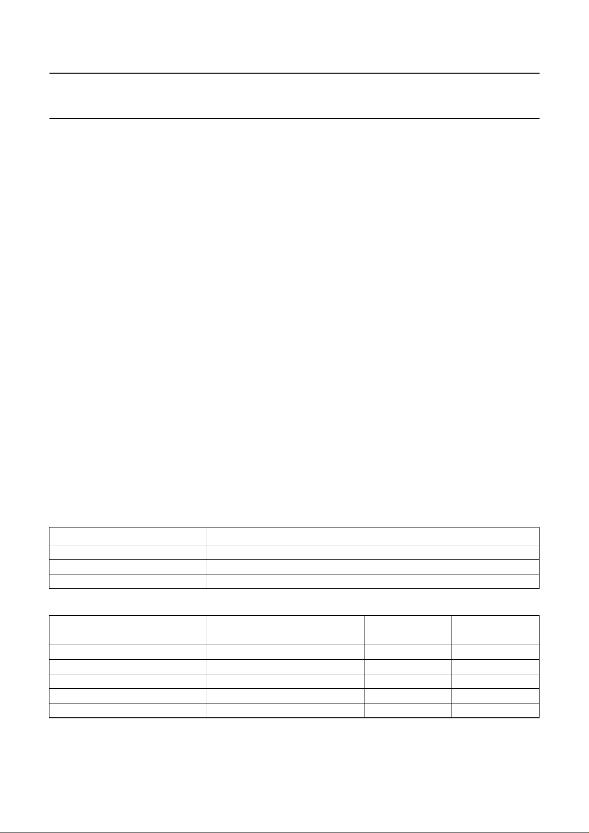
Table 1 Input interface
NAME FUNCTION
ADIN9 to ADIN0 10-bit data input (from external A/D converter)
ADCLK 36 MHz clock signal input
CLK36 clock signal output for sampling incoming data (to external A/D converter)
Table 2 AGC
2
I
FILTER OUTPUT LEVEL COMPARATOR OUTPUT
Above threshold 1 0 1
Below threshold 0 0 0
Above threshold 1 1 0
Below threshold 0 1 1
Equal to threshold Z 0 Z
C-bus
bit AGC_DIR
Pin AGCOUT
2000 May 19 11
 Loading...