

Philips TDA8960H-N1 Datasheet

DATA SH EET
Preliminary specification
File under Integrated Circuits, IC02
1999 Jun 14
INTEGRATED CIRCUITS
TDA8960
ATSC 8-VSB demodulator and
decoder

1999 Jun 14 2
Philips Semiconductors Preliminary specification
ATSC 8-VSB demodulator and decoder TDA8960
FEATURES
General features
• One-chip Advanced Television Systems Committee
(ATSC)-compliant demodulator and concatenated trellis
(Viterbi)/Reed Solomon decoder with de-interleaver and
de-randomizer
• 0.4 µm process
• 3.3 V device
• 64-lead QFP64 package
• Boundary scan test
• Output format: 8-bit wide bus.
8-VSB demodulator
• On-chip digital circuitry for tuner Automatic Gain Control
(AGC)
• Square root raised cosine filter with 11.5% roll-off factor
• Fully internal carrier recovery loop
• Mostly internal clock recovery and AGC loops with
programmable loop filters
• External indication of demodulator lock.
Adaptive equalizer
• Feed forward including a Decision Feedback Equalizer
(DFE) structure
• Range of −2.3 to +10.5 µs
• Adaptation based on ATSC field sync (trained) and/or
8-VSB data (blind)
• Trellis (Viterbi) decoder
• Rate
2
⁄3 (Rate1⁄2Ungerboeck code based).
Reed Solomon decoder
• (207, 187 and T = 10) Reed Solomon code
• Internal convolutional de-interleaving (I = 52; using
internal memory)
• External indication of uncorrectable error; transport error
indicator bit in Motion Picture Export Group (MPEG)
packet header is also set
• Followed by de-randomizer based on ATSC standard.
I
2
C-bus interface
• I2C-bus interface to initialize and monitor the
demodulator and Forward Error Correction (FEC)
decoder. Operation without I2C-bus control is possible
(default).
DOCUMENT REFERENCES
See the ATSC URL on ‘http://www.atsc.com’ for the
following related documents:
•
“ATSC Digital Television Standard”
(document no. A/53,
issued 1995 Sep 16)
•
“Guide to the use of the ATSC Digital Television
Standard”
(document no. A/54, issued 1995 Oct 04).
APPLICATIONS
• Digital ATSC compliant TV receivers
• Personal computers with digital television capabilities
• Set-top boxes.
ORDERING INFORMATION
TYPE
NUMBER
PACKAGE
NAME DESCRIPTION VERSION
TDA8960 QFP64 plastic quad flat package; 64 leads (lead length 1.95 mm); body 14 × 20 × 2.8 mm SOT319-2

1999 Jun 14 3
Philips Semiconductors Preliminary specification
ATSC 8-VSB demodulator and decoder TDA8960
GENERAL DESCRIPTION
The TDA8960 is an ATSC-compliant demodulator and
forward error correction decoder for reception of 8-VSB
modulated signals for terrestrial and cable applications:
• Terrestrial: reception of 8-VSB modulated signals via
standard 6 MHz VHF/UHF terrestrial TV channels
(TV channels 2 to 69 in the United States)
• Cable: reception of 8-VSB modulated signals via
standard 6 MHz VHF/UHF cable TV channels.
Most of the loop components needed to recover the data
from the received symbols are internal. The only required
external loop components are a low-speed serial D/A
converter and a Voltage Controlled crystal Oscillator
(VCXO) for the symbol timing recovery and an opamp
integrator for the AGC. Loop parameters of the clock and
carrier recovery can be controlled by the I
2
C-bus.
A tuner converts the incoming RF frequency to a fixed IF
frequency centred at 44 MHz. The output of the tuner is
filtered, followed by a down conversion in an IF block to a
low IF frequency centred at1⁄2 the VSB symbol rate (or a
frequency of approximately 5.38 MHz). The low IF signal is
applied to the A/D converter.
To use its full input span, the A/D converter is located
within what is typically a fine AGC loop which includes a
variable gain stage at the output of the IF block. However,
it is also possible to apply the TDA8960 AGC control
output directly to the tuner. The detector for the TDA8960
AGC output is located after the A/D converter and
determines the peak level of the incoming signals. After
gain control, the low IF signal is sampled at a nominal rate
of twice the VSB symbol frequency, or approximately
21.5 MHz.
The carrier recovery is performed completely internally.
This function consists of a digital frequency and Frequency
Phase-Locked Loop (FPLL).
Data shaping is performed with a square root raised cosine
(half Nyquist) filter with roll-off factor of 11.5%.
Symbol timing recovery is performed mostly within the
TDA8960, except that a low cost D/A converter and VCXO
are required externally to generate the nominal 21.52 MHz
clock signal for the A/D converter and TDA8960.
After carrier recovery, half Nyquist filtering and symbol
timing recovery, adaptive equalization is performed based
on the use of the ATSC field sync (trained equalization)
and/or the 8-VSB data itself (blind equalization).
The adaptive equalizer uses a DFE structure.
After trellis decoding, the stream is de-interleaved with a
convolutional de-interleaver (interleaving depth 52).
The memory for de-interleaving is on-chip. The Reed
Solomon decoder is A TSC-compliant with a length of 207
and can correct up to 10 bytes. The decoded stream is
de-randomized using a Pseudo Random Bit Sequence
(PRBS). Finally the data is passed to a First-In, First-Out
(FIFO) register that prevents the appearance of irregular
gaps in the output data.
The output of the TDA8960 is an A TSC-compliant MPEG-2
packet stream together with a clock. Furthermore some
signal flags are provided to indicate the sync bytes and the
valid data bytes. Uncorrected blocks are also indicated.
The 8-bit wide MPEG-2 stream can be applied to an
MPEG-2 transport demultiplexer.
1999 Jun 14 4
Philips Semiconductors Preliminary specification
ATSC 8-VSB demodulator and decoder TDA8960
QUICK REFERENCE DATA
Note
1. This corresponds to 12 training sequences.
SYMBOL PARAMETER CONDITIONS MIN. TYP. MAX. UNIT
V
DDD
digital supply voltage 3.0 3.3 3.6 V
I
DDD(tot)
total digital supply current V
DDD
= 3.3 V − 300 − mA
f
clk
clock frequency − 21.52 − MHz
f
sym
symbol frequency − 10.76 − Msymbols/s
IL implementation loss −−−dB
α
ro
half Nyquist filter roll-off factor − 11.5 − %
t
acq
acquisition time note 1 −−290 ms
T
amb
ambient temperature −20 − +70 °C
P
tot
total power dissipation − 1.0 − W
1999 Jun 14 5
Philips Semiconductors Preliminary specification
ATSC 8-VSB demodulator and decoder TDA8960
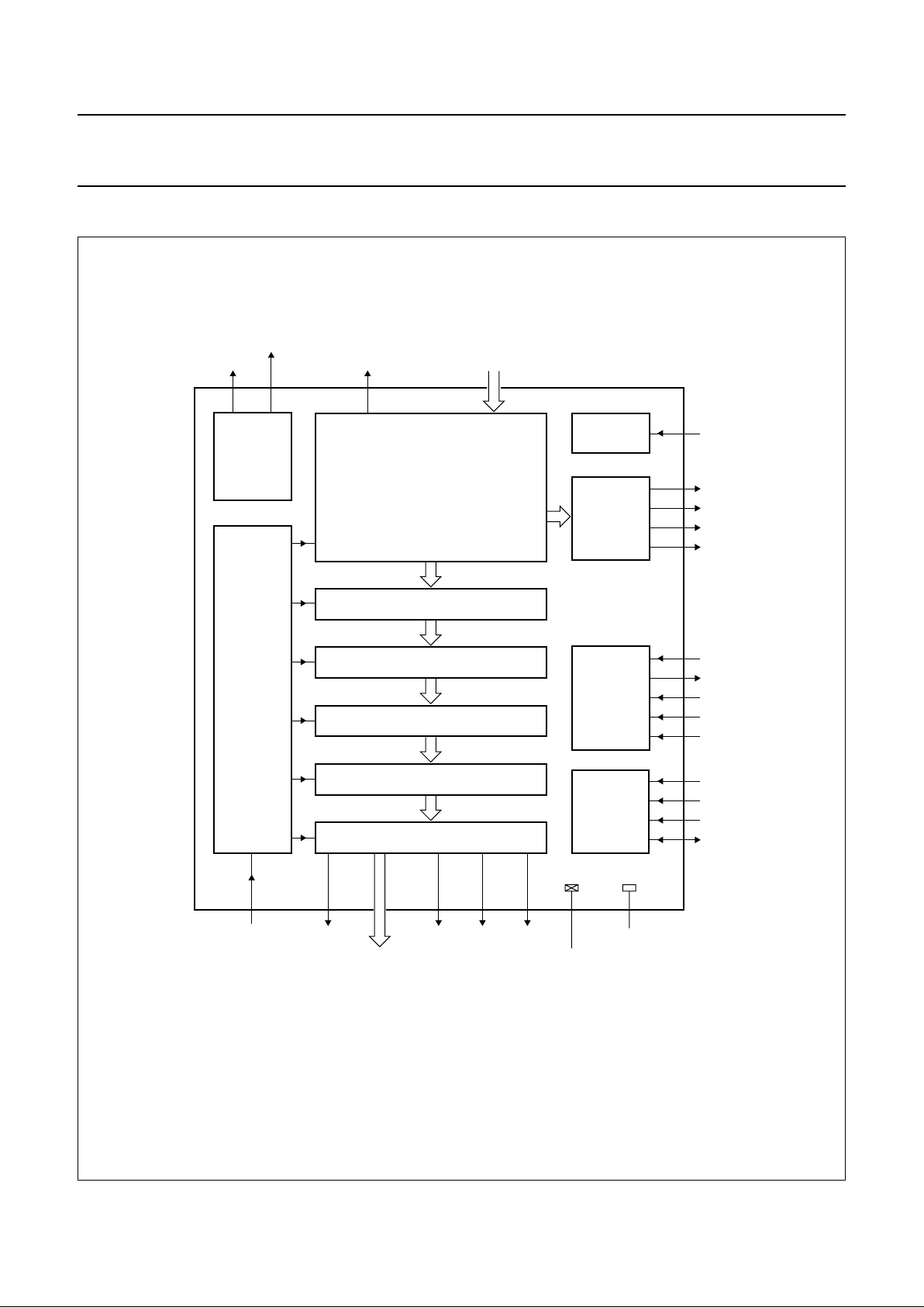
BLOCK DIAGRAM
Fig.1 Block diagram.
- Symbol timing recovery
- Sync recovery and pilot removal
- Adaptive equalization.
(1) The digital front-end consists of the following circuits:
- Fine AGC
- Carrier recovery
- Half Nyquist filter
MGR598
handbook, full pagewidth
29
31 to 33
35 to 37
39, 40
22 24 25
15
14
16
13
19
18
20
21
17
64
63
62
61
27
I2C-BUS
INTERFACE
BOUNDARY
SCAN TEST
SERIAL
DAC
INTERFACE
RESET
TDA8960
FIFO
DE-RANDOMIZER
REED SOLOMON DECODER
DE-INTERLEAVER
TRELLIS DECODER
DIGITAL FRONT-END
(1)
SYNCHRO-
NIZATION
LOCK
DETECTORS
DATACLK
59
CLK
DATA7 to DATA0
V
SSD1
to V
SSD8
V
DDD1
to V
DDD8
ERROR SOP DATAVALID
56 1 to 8, 11, 125453
AGCOUT
EQLOCKINDIC
LOCKINDIC
ADIN0 to ADIN9
TRLD
TRCS
TRSTB
TRSDO
RSTAN
A0
TDI
TMS
TCK
SCL
SDA
A1
TRST
TDO
23, 34,
45, 57,
9, 26,
41, 60
30, 38,
49,55,
10, 28,
42, 58
1999 Jun 14 6
Philips Semiconductors Preliminary specification
ATSC 8-VSB demodulator and decoder TDA8960
PINNING
SYMBOL PIN I/O DESCRIPTION
ADIN0 1 I data input bit 0 from ADC
ADIN1 2 I data input bit 1 from ADC
ADIN2 3 I data input bit 2 from ADC
ADIN3 4 I data input bit 3 from ADC
ADIN4 5 I data input bit 4 from ADC
ADIN5 6 I data input bit 5 from ADC
ADIN6 7 I data input bit 6 from ADC
ADIN7 8 I data input bit 7 from ADC
V
DDD5
9 − digital supply voltage 5 (3.3 V)
V
SSD5
10 − digital core ground 5
ADIN8 11 I data input bit 8 from ADC
ADIN9 12 I data input bit 9 from ADC
A0 13 I I
2
C-bus slave address bit 0
SCL 14 I I
2
C-bus clock
SDA 15 I/O I
2
C-bus serial data
A1 16 I I
2
C-bus slave address bit 1
TDI 17 I TAP controller data input; note 1
TMS 18 I TAP controller test mode select; note 1
TCK 19 I TAP controller test clock; note 1
TRST 20 I TAP controller asynchronous reset; note 1
TDO 21 O TAP controller test data output (3-state); note 1
ERROR 22 O transport packet block error signal
V
DDD1
23 − digital supply voltage 1 (3.3 V)
SOP 24 O start of transport packet signal
DATAVALID 25 O transport packet data valid signal
V
DDD6
26 − digital supply voltage 6 (3.3 V)
RSTAN 27 I asynchronous reset
V
SSD6
28 − digital ground 6
DATACLK 29 O transport interface data clock
V
SSD1
30 − digital ground 1
DATA7 31 O transport packet data output bit 7
DATA6 32 O transport packet data output bit 6
DATA5 33 O transport packet data output bit 5
V
DDD2
34 − digital supply voltage 2 (3.3 V)
DATA4 35 O transport packet data output bit 4
DATA3 36 O transport packet data output bit 3
DATA2 37 O transport packet data output bit 2
V
SSD2
38 − digital ground 2
DATA1 39 O transport packet data output bit 1
DATA0 40 O transport packet data output bit 0
1999 Jun 14 7
Philips Semiconductors Preliminary specification
ATSC 8-VSB demodulator and decoder TDA8960
Note
1. In accordance with the
“IEEE 1149.1”
standard; pads TCK, TDI, TMS and TRST are input pads with an internal
pull-up transistor and pad TDO is a 3-state output pad.
V
DDD7
41 − digital supply voltage 7 (3.3 V)
V
SSD7
42 − digital ground 7
n.c. 43 not connected
n.c. 44 not connected
V
DDD3
45 − digital supply voltage 3 (3.3 V)
n.c. 46 not connected
n.c. 47 not connected
n.c. 48 not connected
V
SSD3
49 − digital ground 3
n.c. 50 not connected
n.c. 51 not connected
n.c. 52 not connected
LOCKINDIC 53 O lock indicator of front-end
EQLOCKINDIC 54 O lock indicator of equalizer
V
SSD4
55 − digital ground 4
AGCOUT 56 O AGC control signal (3-state)
V
DDD4
57 − digital supply voltage 4 (3.3 V)
V
SSD8
58 − digital ground 8
CLK 59 I clock
V
DDD8
60 − digital supply voltage 8 (3.3 V)
TRSDO 61 O serial data to DAC
TRSTB 62 O strobe signal to DAC
TRCS 63 O chip select signal to DAC
TRLD 64 O load signal to DAC
SYMBOL PIN I/O DESCRIPTION
1999 Jun 14 8
Philips Semiconductors Preliminary specification
ATSC 8-VSB demodulator and decoder TDA8960
Fig.2 Pin configuration.
handbook, full pagewidth
TDA8960
MGR599
1
2
3
4
5
6
7
8
9
10
11
12
13
14
15
16
17
18
19
ADIN0
ADIN1
ADIN2
ADIN3
ADIN4
ADIN5
ADIN6
ADIN7
V
DDD5
V
SSD5
ADIN8
ADIN9
A0
TDI
TMS
TCK
SCL
SDA
A1
n.c.
n.c.
V
SSD3
n.c.
n.c.
n.c.
V
DDD3
n.c.
n.c.
V
SSD7
V
DDD7
DATA0
DATA1
V
SSD2
DATA2
DATA3
DATA4
V
DDD2
DATA5
51
50
49
48
47
46
45
44
43
42
41
40
39
38
37
36
35
34
33
20
21
22
23
24
25
26
27
28
29
30
31
32
64
63
62
61
60
59
58
57
56
55
54
53
52
TRLD
TRCS
TRSTB
TRSDO
V
DDD8
CLK
V
SSD8
V
DDD4
AGCOUT
V
SSD4
EQLOCKINDIC
LOCKINDIC
n.c.
TRST
TDO
ERROR
V
DDD1
SOP
DATAVALID
V
DDD6
RSTAN
V
SSD6
DATACLK
V
SSD1
DATA7
DATA6
1999 Jun 14 9
Philips Semiconductors Preliminary specification
ATSC 8-VSB demodulator and decoder TDA8960
FUNCTIONAL DESCRIPTION
The internal architecture of the TDA8960 consists of
basically two parts:
• The front-end containing the AGC, carrier recovery, half
Nyquist filter, symbol timing recovery, sync recovery and
adaptive equalization
• The back-end containing the trellis decoder,
de-interleaver, the Reed Solomon decoder and
de-randomizer.
AGC
This block controls an analog gain over a range of up to
±20 dB.
The data from the A/D converter (Philips Semiconductors’
TDA8763 is recommended) arrives at the VSB
demodulator via inputs ADIN9 to ADIN0, which is10-bit
wide. The format of the incoming samples can be
programmed using the I
2
C-bus accessible register 08H.
By writing to bit 3 the format can be either twos
complement or binary.
The absolute value of the input signal is averaged over
several samples. The filtered signal is compared to a
threshold. The threshold consist of a 4-bit signed value
which can be programmed using the I2C-bus. The 3-state
output signal charges or discharges an off-chip ideal
integrator and is used to control the gain controller of the
tuner front-end module. The values of the signal are shown
in Table 1.
Table 1 AGC output
The analog low-pass filter or integrator circuit should be
designed with an 8 ms time constant. The response of the
gain amplifier is linear with respect to the control voltage
over the desired range of operation.
Carrier recovery
This circuit recovers the frequency and phase of the pilot
carrier. The spectrum during the carrier recovery is
displayed in Fig.3.
PIN AGCOUT COMMENT
1 output of the filter is smaller than the
threshold
0 output of the filter is larger than the
threshold
Z output of the filter is equal to the
threshold
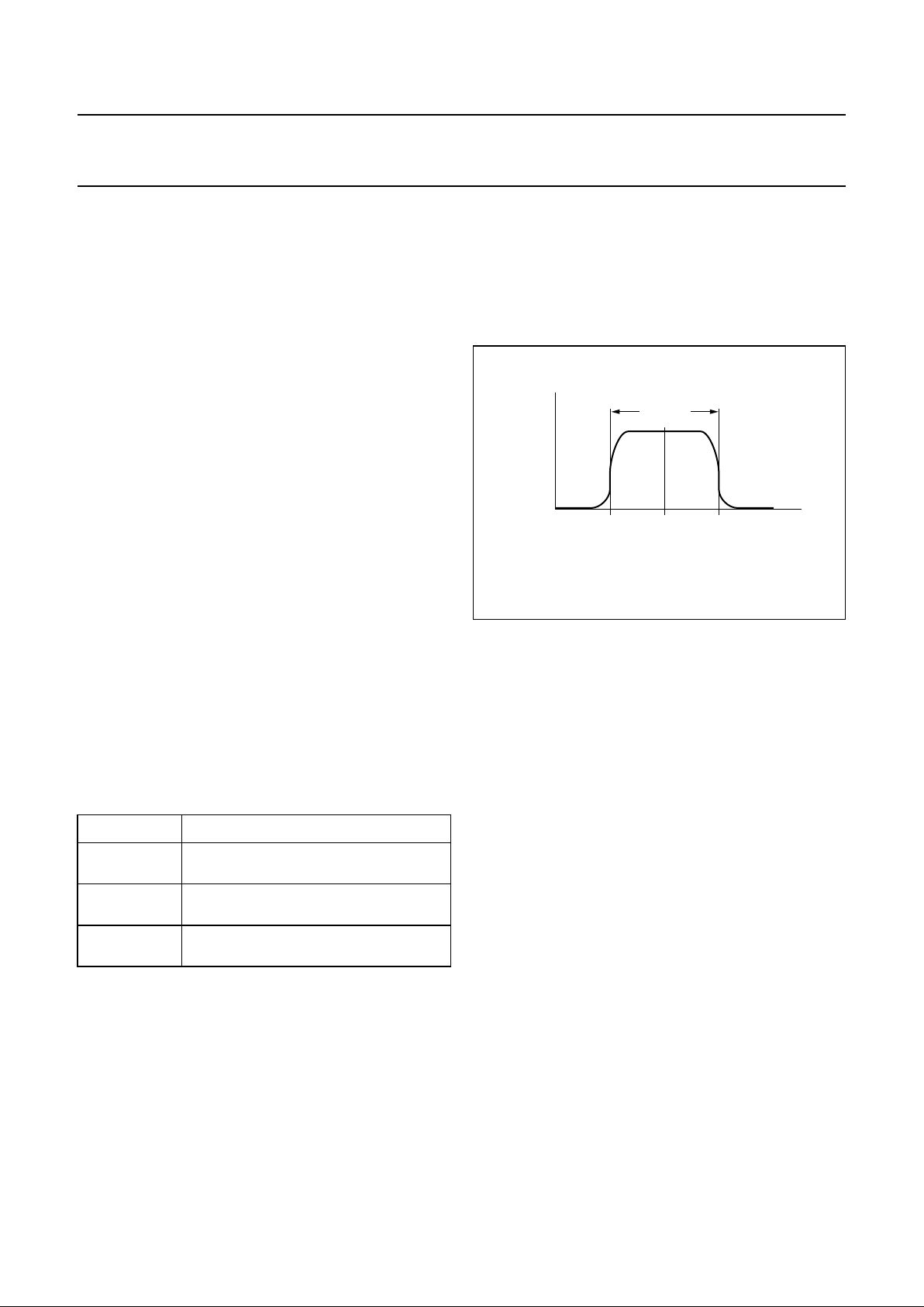
By default the carrier is present at 2.69 MHz. During carrier
recovery a shift is applied such that the pilot is present at
DC. It can happen that the pilot is present at the higher
edge of the VSB spectrum. In this event the CR_INV bit in
I2C-bus register 08H (see Table 13) can be set to make
sure that after the shift the pilot is at DC.
The carrier recovery is capable of tracking a frequency
offset of up to 100 kHz from the nominal frequency offset
within 100 ms.
By means of I2C-bus read register 03H the current
frequency offset in the carrier recovery can be read.
This value can be used for fine tuning applications.
Sync recovery and pilot removal
This block performs several functions including pilot
removal, segment and field sync removal and rescale
AGC based on the segment sync. If this block is able to
find a data segment sync signal, the external pin
LOCKINDIC is asserted. The value of this signal can also
be read through I
2
C-bus control.
Adaptive equalization
The equalizer consists of a forward filter and a feedback
filter section. Demodulated symbols from the
synchronization and pilot removal block are received every
symbol period. The equalizer tries to invert the effects of
the channel on the transmitted symbol stream by filtering
these symbols. The coefficients of the filters are updated
every symbol period using the training sequence. There is
also a provision to perform blind equalization. The filtered
output is available for the next block, the trellis decoder.
Fig.3 Signal spectrum during carrier recovery.
handbook, halfpage
MGR600
amplitude
(dB)
frequency (MHz)
5.38 MHz
2.69 5.38 8.07

1999 Jun 14 10
Philips Semiconductors Preliminary specification
ATSC 8-VSB demodulator and decoder TDA8960
The equalizer has been designed to correct a maximum
pre-echo of 2.32 µs and a maximum post-echo of
10.50 µs. The equalizer uses an overlapping DFE to
reduce the effects of co-channel interference.
The equalizer has been optimized to have a typical
acquisition time of 12 training sequences, which
corresponds to approximately 290 ms. The acquisition
time has been defined as the time when the output
signal-to-noise ratio reaches the Threshold Of Visibility
(TOV). The ATSC defines a TOV of 14.9 dB for 8-VSB.
Based on the training signal and the output of the equalizer
the Mean Square Error (MSE) signal is generated. This
16-bit value is used to control the channel adaptation
process and is available though I2C-bus control.
Control
The TDA8960 contains a complicated finite state machine.
This state machine controls the sequence of operations
that must be performed when a valid VSB data signal is
detected in order for it to be properly decoded into a
stream of MPEG-2 transport packets. The following steps
have to take place:
1. The external tuner is directed to lock to a specified
channel frequency. A VSB signal is present.
2. The tuner AGC locks to an acceptable signal gain.
3. The coarse AGC of the TDA8960 locks to acceptable
A/D converter gain.
4. The timing and carrier recovery loops lock to the
symbol clock and the carrier frequency.
5. The segment sync pattern is detected. The segment
sync lock is acquired.
6. The fine AGC locks.
7. The field sync pattern is detected. The MSE of the
received field sync training sequence is determined.
8. The equalizer uses subsequent training sequences to
adapt itself to the channel conditions.
9. The equalizer adapts to the point that the MSE of the
training sequence is sufficiently small. The trellis
decoding, convolutional de-interleaving and Reed
Solomon decoding processes all begin.
10. Valid MPEG-2 transport packets are generated.
The finite state machine consists of three states. After a
reset has been applied, the state machine starts in state 0.
S
TATE 0: CHANNEL ACQUISITION
In this state either no channel signal is present or a
channel signal is being acquired. The AGC, timing
recovery and carrier recovery loops must first lock onto it.
If the segment sync lock is lost, pin LOCKINDIC is LOW,
or a hardware reset is applied to the VSB demodulator, the
finite state machine returns to state 0.
S
TATE 1: EQUALIZER TRAINING
The finite state machine remains in state 1 until the MSE
of the equalized training sequence falls below a certain
threshold. It should be noted that in state 1 the back-end is
continuously reset to make sure that after the demodulator
has locked onto a signal, the trellis decoder and following
processing blocks begin at the start of the next complete
data field. By means of I2C-bus registers 01H and 02H the
MSE value of the equalizer can be read. This value can be
used for applications such as antenna pointing.
S
TATE 2: NORMAL OPERATION
Normally the state machine would remain in state 2 as
long as no synchronization error occurs. If the MSE of the
equalized training sequence is exceeded for more than
100 ms, the equalizer is reset for one symbol period and
the adaptation process starts again. If the demodulator is
in this state, the EQLOCKINDIC pin signal goes up.
The value of this signal can also be read through the
I2C-bus.
 Loading...