

Page 1

DATA SH EET
Objective specification 2003 Mar 20
TDA8922
2 × 25 W class-D power amplifier
INTEGRATED CIRCUITS
Page 2

2003 Mar 20 2
Philips Semiconductors Objective specification
2 × 25 W class-D power amplifier TDA8922
CONTENTS
1 FEATURES
2 APPLICATIONS
3 GENERAL DESCRIPTION
4 QUICK REFERENCE DATA
5 ORDERING INFORMATION
6 BLOCK DIAGRAM
7 PINNING
8 FUNCTIONAL DESCRIPTION
8.1 General
8.2 Pulse width modulation frequency
8.3 Protections
8.3.1 Overtemperature
8.3.2 Short-circuit acrossloudspeaker terminals and
to supply lines
8.3.3 Start-up safety test
8.3.4 Supply voltage alarm
8.4 Differential audio inputs
9 LIMITING VALUES
10 THERMAL CHARACTERISTICS
11 QUALITY SPECIFICATION
12 STATIC CHARACTERISTICS
13 SWITCHING CHARACTERISTICS
14 DYNAMICAC CHARACTERISTICS(STEREO
AND DUAL SE APPLICATION)
15 DYNAMIC AC CHARACTERISTICS (MONO
BTL APPLICATION)
16 APPLICATION INFORMATION
16.1 BTL application
16.2 Pin MODE
16.3 Output power estimation
16.4 External clock
16.5 Heatsink requirements
16.6 Output current limiting
16.7 Pumping effects
16.8 Reference design
16.9 PCB information for HSOP24 package
16.10 Classification
16.11 Bill of materials for reference design
16.12 Curves measured in reference design
16.13 Application schematics
17 PACKAGE OUTLINE
18 SOLDERING
18.1 Introduction
18.2 Through-hole mount packages
18.2.1 Soldering by dipping or by solder wave
18.2.2 Manual soldering
18.3 Surface mount packages
18.3.1 Reflow soldering
18.3.2 Wave soldering
18.3.3 Manual soldering
18.4 Suitability of IC packages for wave, reflow and
dipping soldering methods
19 DATA SHEET STATUS
20 DEFINITIONS
21 DISCLAIMERS
Page 3

2003 Mar 20 3
Philips Semiconductors Objective specification
2 × 25 W class-D power amplifier TDA8922
1 FEATURES
• High efficiency (∼90%)
• Operating supply voltage from ±12.5 to ±30 V
• Very low quiescent current
• Low distortion
• Usable as a stereo Single-Ended (SE) amplifier or as a
mono amplifier in Bridge-Tied Load (BTL)
• Fixed gain of 30 dB in Single-Ended (SE) and 36 dB in
Bridge-Tied Load (BTL)
• High output power
• Good ripple rejection
• Internal switching frequency can be overruled by an
external clock
• No switch-on or switch-off plop noise
• Short-circuit proof across load and to supply lines
• Electrostatic discharge protection
• Thermally protected.
2 APPLICATIONS
• Television sets
• Home-sound sets
• Multimedia systems
• All mains fed audio systems
• Car audio (boosters).
3 GENERAL DESCRIPTION
The TDA8922 is a high efficiency class-D audio power
amplifier with very low dissipation. The typical output
power is 2 × 25 W.
The device is available in the HSOP24 power package
with a small internal heatsink and in the DBS23P
through-hole power package. Depending on the supply
voltage and load conditions, a very small or even no
external heatsink is required. The amplifier operates over
a wide supply voltage range from ±12.5 to ±30 V and
consumes a very low quiescent current.
4 QUICK REFERENCE DATA
Note
1. See Section 16.5.
5 ORDERING INFORMATION
SYMBOL PARAMETER CONDITIONS MIN. TYP. MAX. UNIT
General; VP= ±20 V
V
P
supply voltage ±12.5 ±20 ±30 V
I
q(tot)
total quiescent supply
current
no load connected − 55 75 mA
η efficiency P
o
= 25 W; SE: RL=2×8Ω; fi= 1 kHz − 90 − %
Stereo single-ended configuration
P
o
output power RL=8Ω; THD = 10%; VP= ±20 V; note 1 22 25 − W
R
L
=4Ω; THD = 10%; VP= ±15 V; note 1 22 25 − W
Mono bridge-tied load configuration
P
o
output power RL=8Ω; THD = 10%; VP= ±15 V; note 1 46 50 − W
TYPE
NUMBER
PACKAGE
NAME DESCRIPTION VERSION
TDA8922TH HSOP24 plastic, heatsink small outline package; 24 leads;
low stand-off height
SOT566-3
TDA8922J DBS23P plastic DIL-bent-SIL power package; 23 leads
(straight lead length 3.2 mm)
SOT411-1
Page 4
2003 Mar 20 4
Philips Semiconductors Objective specification
2 × 25 W class-D power amplifier TDA8922
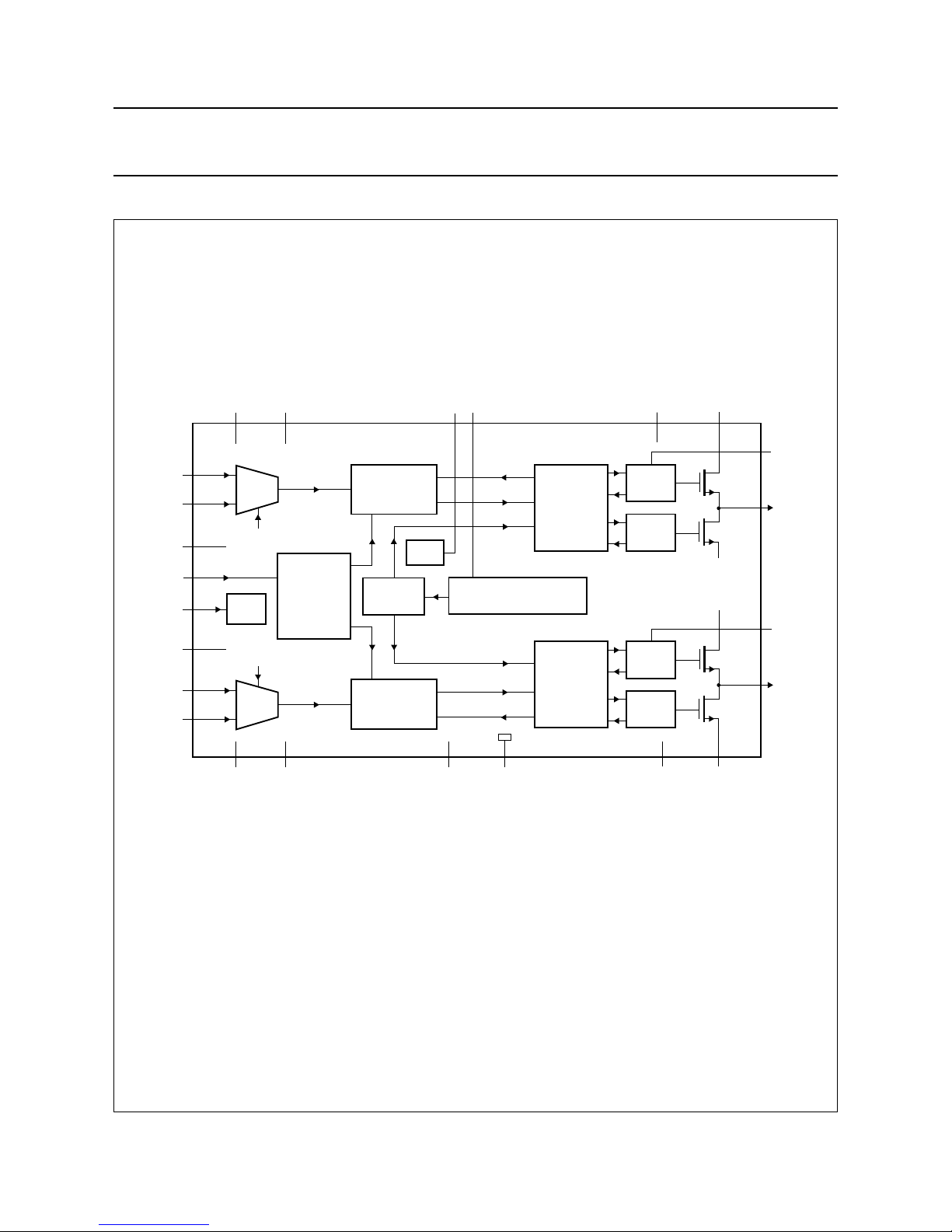
6 BLOCK DIAGRAM
handbook, full pagewidth
MGU994
OUT1
V
SSP1
V
DDP2
DRIVER
HIGH
OUT2
BOOT2
TDA8922TH
(TDA8922J)
BOOT1
DRIVER
LOW
RELEASE1
SWITCH1
ENABLE1
CONTROL
AND
HANDSHAKE
PWM
MODULATOR
MANAGER
OSCILLATOR
TEMPERATURE SENSOR
CURRENT PROTECTION
STABI
MODE
INPUT
STAGE
mute
9 (3)
8 (2)
IN1−
IN1+
22 (15)
21 (14)
20 (13)
17 (11)
16 (10)
15 (9)
V
SSP2
V
SSP1
DRIVER
HIGH
DRIVER
LOW
RELEASE2
SWITCH2
ENABLE2
CONTROL
AND
HANDSHAKE
PWM
MODULATOR
11 (5)
SGND1
7 (1)
OSC
2 (19)
SGND2
6 (23)
MODE
INPUT
STAGE
mute
5 (22)
4 (21)
IN2−
IN2+
19 (-)24 (17)
V
SSD
HW
(1)
1 (18)
V
SSA2
12 (6)
V
SSA1
3 (20)
V
DDA2
10 (4)
V
DDA1
23 (16)13 (7)18 (12) 14 (8)
V
DDP2
PROTSTABI
V
DDP1
Fig.1 Block diagram.
(1) Pin HW (TDA8922TH only) should be connected to pin V
SSD
in the application.
Pin numbers in parenthesis refer to the TDA8922J.
Page 5

2003 Mar 20 5
Philips Semiconductors Objective specification
2 × 25 W class-D power amplifier TDA8922
7 PINNING
SYMBOL
PIN
DESCRIPTION
TDA8922TH TDA8922J
V
SSA2
1 18 negative analog supply voltage for channel 2
SGND2 2 19 signal ground for channel 2
V
DDA2
3 20 positive analog supply voltage for channel 2
IN2− 4 21 negative audio input for channel 2
IN2+ 5 22 positive audio input for channel 2
MODE 6 23 mode selection input: standby, mute or operating
OSC 7 1 oscillator frequency adjustment or tracking input
IN1+ 8 2 positive audio input for channel 1
IN1− 9 3 negative audio input for channel 1
V
DDA1
10 4 positive analog supply voltage for channel 1
SGND1 11 5 signal ground for channel 1
V
SSA1
12 6 negative analog supply voltage for channel 1
PROT 13 7 time constant capacitor for protection delay
V
DDP1
14 8 positive power supply voltage for channel 1
BOOT1 15 9 bootstrap capacitor for channel 1
OUT1 16 10 PWM output from channel 1
V
SSP1
17 11 negative power supply voltage for channel 1
STABI 18 12 decoupling of internal stabilizer for logic supply
HW 19 − handle wafer; must be connected to pin V
SSD
V
SSP2
20 13 negative power supply voltage for channel 2
OUT2 21 14 PWM output from channel 2
BOOT2 22 15 bootstrap capacitor for channel 2
V
DDP2
23 16 positive power supply voltage for channel 2
V
SSD
24 17 negative digital supply voltage
Page 6
2003 Mar 20 6
Philips Semiconductors Objective specification
2 × 25 W class-D power amplifier TDA8922
handbook, halfpage
MGU995
HW
PROT
BOOT1
V
DDP1
V
SSP1
OUT1
BOOT2
V
SSP2
OUT2
V
SSD
V
DDP2
STABI
MODE
V
SSA1
V
DDA1
SGND1
IN1+
IN1−
V
DDA2
IN2+
IN2−
V
SSA2
SGND2
OSC
TDA8922TH
1
2
3
4
5
6
7
8
9
10
11
12
24
23
22
21
20
19
18
17
16
15
14
13
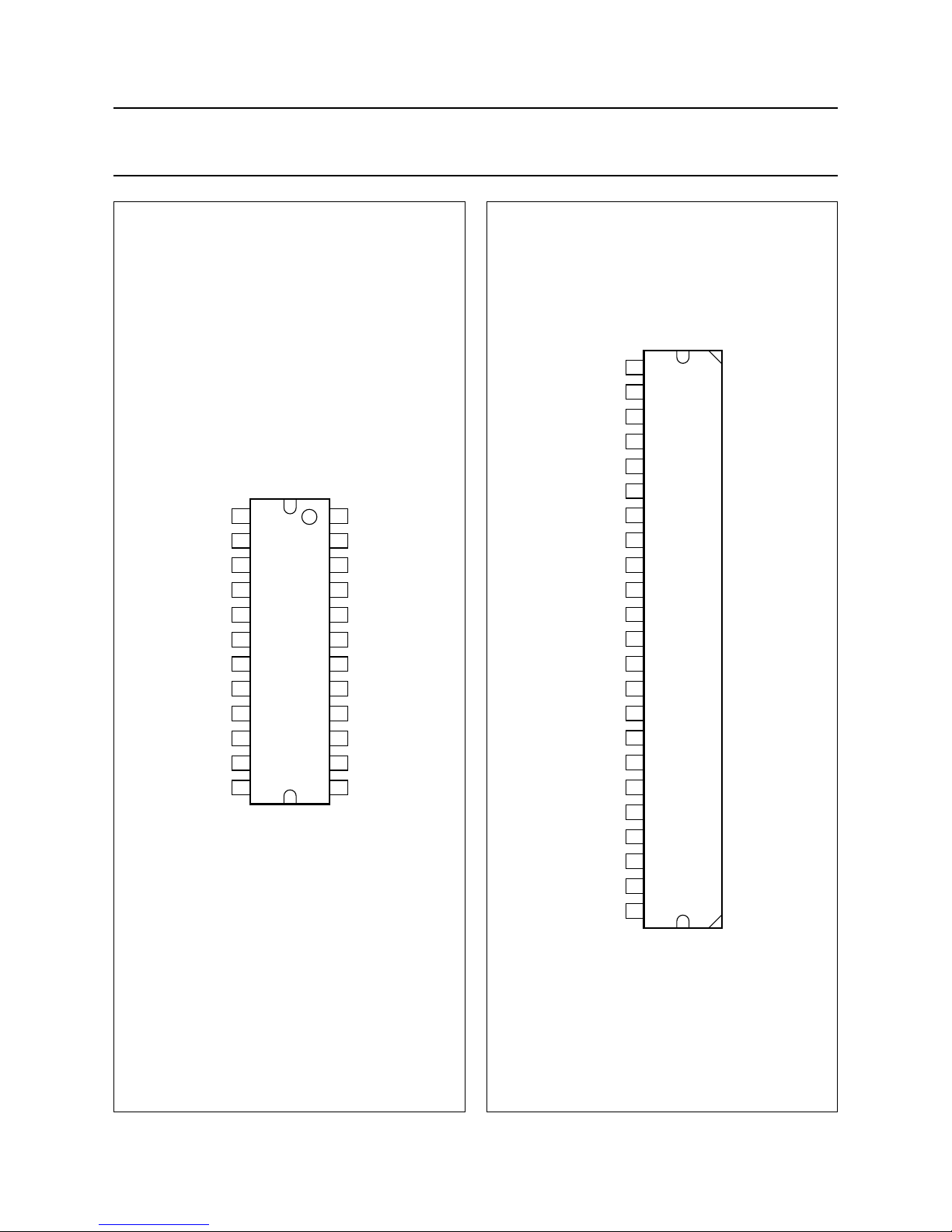
Fig.2 Pin configuration TDA8922TH.
handbook, halfpage
TDA8922J
MGU996
1
2
3
4
5
6
7
8
9
10
11
12
13
14
15
16
17
18
19
20
21
22
23
PROT
BOOT1
V
DDP1
V
SSP1
OUT1
BOOT2
V
SSP2
OUT2
V
SSD
V
DDP2
STABI
MODE
V
SSA1
V
DDA1
SGND1
IN1+
IN1−
V
DDA2
IN2+
IN2−
V
SSA2
SGND2
OSC
Fig.3 Pin configuration TDA8922J.
Page 7
2003 Mar 20 7
Philips Semiconductors Objective specification
2 × 25 W class-D power amplifier TDA8922
8 FUNCTIONAL DESCRIPTION
8.1 General
TheTDA8922isatwochannelaudiopoweramplifierusing
class-D technology. A detailed application reference
design is shown in Fig.10. Typical application schematics
are shown in Figs 37 and 38.
The audio input signal is converted into a digital Pulse
Width Modulated (PWM) signal via an analog input stage
and PWM modulator. To enable the output power
transistors to be driven, this digital PWM signal is applied
to a control and handshake block and driver circuits for
both the high side and low side. In this way a level shift is
performed from the low power digital PWM signal
(at logic levels) to a high power PWM signal which
switches between the main supply lines.
A 2nd-order low-pass filter converts the PWM signal to an
analog audio signal across the loudspeakers.
The TDA8922 one-chip class-D amplifier contains high
power D-MOS switches, drivers, timing and handshaking
between the power switches and some control logic. For
protection a temperature sensor and a maximum current
detector are built-in.
The two audio channels of the TDA8922 contain two
PWMs, two analog feedback loops and two differential
input stages. It also contains circuits common to both
channels such as the oscillator, all reference sources, the
mode functionality and a digital timing manager.
The TDA8922 contains two independent amplifier
channels with high output power, high efficiency (90%),
low distortion and a low quiescent current. The amplifier
channels can be connected in the following configurations:
• Mono Bridge-Tied Load (BTL) amplifier
• Stereo Single-Ended (SE) amplifiers.
The amplifier system can be switched in three operating
modes with pin MODE:
• Standby mode; with a very low supply current
• Mute mode; the amplifiers are operational, but the audio
signal at the output is suppressed
• Operating mode; the amplifiers fully are operational with
output signal.
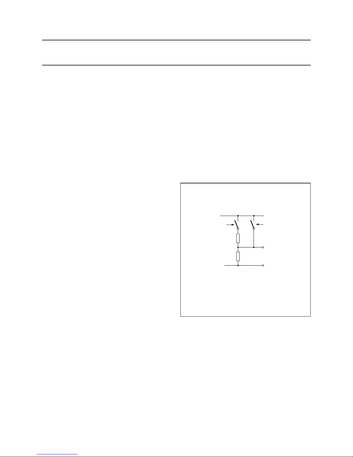
An example of a switching circuit for driving pin MODE is
illustrated in Fig.4.
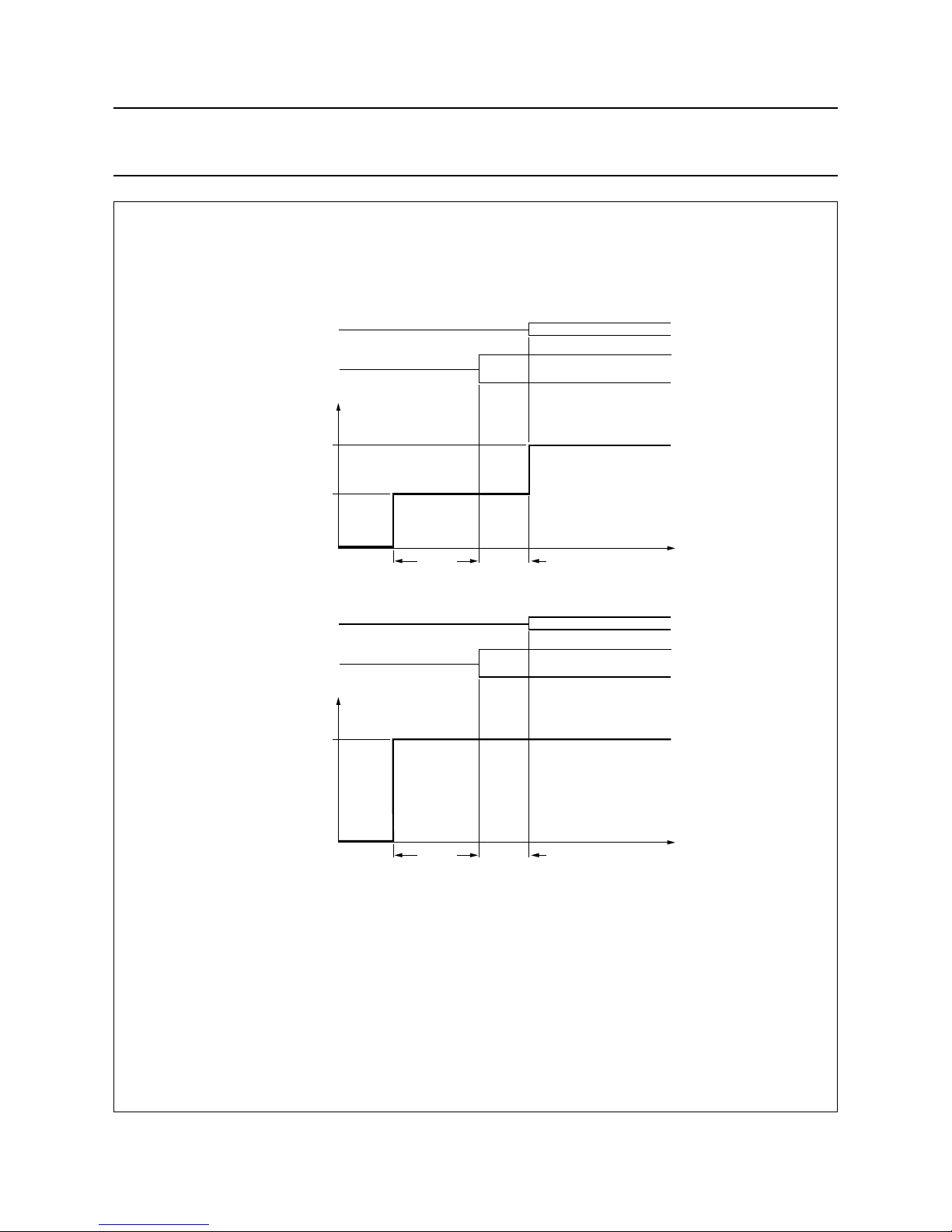
For suppressing plop noise, the amplifier will remain
automatically in the mute mode for approximately 150 ms
before switching to the operating mode (see Fig.5).
During this time, the coupling capacitors at the input are
fully charged.
handbook, halfpage
standby/
mute
R
R
mute/on
MODE pin
SGND
MBL463
+5 V
Fig.4 Example of mode selection circuit.
Page 8
2003 Mar 20 8
Philips Semiconductors Objective specification
2 × 25 W class-D power amplifier TDA8922
handbook, full pagewidth
audio
operating
mute
standby
4 V
2 V
0 V (SGND)
time
V
mode
100 ms >50 ms
switching
audio
operating
standby
4 V
0 V (SGND)
time
MBL465
V
mode
100 ms 50 ms
switching
Fig.5 Timing on mode selection input.
When switchingfromstandby to mute, there is a delay of 100 ms before theoutput starts switching.The audio signal is available after V
mode
has been
set to operating, but not earlier than 150 ms after switching to mute.
When switching from standby to operating, there is a first delay of 100 ms before the outputs starts switching. The audio signal is available after a
second delay of 50 ms.
Page 9

2003 Mar 20 9
Philips Semiconductors Objective specification
2 × 25 W class-D power amplifier TDA8922
8.2 Pulse width modulation frequency
The output signal of the amplifier is a PWM signal with a
carrier frequency of approximately 350 kHz. Using a
2nd-order LC demodulation filter in the application results
in an analog audio signal across the loudspeaker.
This switching frequency is fixed by an external resistor
R
OSC
connected between pin OSC and V
SSA
. With the
resistor value given in the schematic diagram of the
reference design, the carrier frequency is typical 350 kHz.
The carrier frequency can be calculated using the
following equation:
If two or more class-D amplifiers are used in the same
audio application, it is advisable to have all devices
operating at the same switching frequency.
This can be realized by connecting all OSC pins together
and feed them from a external central oscillator. Using an
external oscillator it is necessary to force pin OSC to a
DC-level above SGND for switching from the internalto an
external oscillator. In this case the internal oscillator is
disabled and the PWM will be switched on the external
frequency. The frequency range of the external oscillator
must be in the range as specified in the switching
characteristics; see Chapter 13.
In an application circuit:
• Internal oscillator: R
OSC
connected between pin OSC
and V
SSA
• Externaloscillator:connecttheoscillator signal between
pins OSC and SGND; delete R
OSC
and C
OSC
.
8.3 Protections
Temperature, supply voltage and short-circuit protections
sensors are included on the chip. In the event that the
maximum current or maximum temperature is exceeded
the system will shut down.
8.3.1 OVERTEMPERATURE
If the junction temperature Tj> 150 °C, then the power
stage will shut down immediately. The power stage will
start switching again if the temperature drops to
approximately 130 °C, thus there is a hysteresis of
approximately 20 °C.
8.3.2 S
HORT-CIRCUIT ACROSS LOUDSPEAKER TERMINALS
AND TO SUPPLY LINES
When the loudspeaker terminals are short-circuited or if
one of the demodulated outputs of the amplifier is
short-circuited to one of the supply lines, this will be
detected by the current protection. If the output current
exceeds the maximum output current of 4 A, then the
power stage will shut down within less than 1 µs and the
high current will be switched off. In this state the
dissipation is very low. Every 100 ms the system tries to
restart again. If there is still a short-circuit across the
loudspeaker load or to one of the supply lines, the system
is switched off again as soon as the maximum current is
exceeded. The average dissipation will be low because of
this low duty cycle.
8.3.3 START-UP SAFETY TEST
Duringthestart-upsequence,whenpin MODEisswitched
from standby to mute, the conditions at the output
terminals of the power stage are checked. In the event of
a short-circuit at one of the output terminals to VDDor V
SS
thestart-upprocedureisinterruptedand the systems waits
for open-circuit outputs. Because the test is done before
enablingthepowerstages,nolargecurrentswill flow in the
event of a short-circuit. This system protects for
short-circuitsatbothsidesoftheoutput filter to both supply
lines. When there is a short-circuit from the power PWM
outputof the power stage to oneof the supply lines (before
the demodulation filter) it will also be detected by the
start-upsafety test. Practical use of thistest feature can be
found in detection of short-circuits on the printed-circuit
board.
Remark: This test is only operational prior to or during the
start-up sequence, and not during normal operation.
During normal operation the maximum current protection
is used to detect short-circuits across the load and with
respect to the supply lines.
f
osc
910
9
×
R
OSC
------------------ -
Hz=
Page 10
2003 Mar 20 10
Philips Semiconductors Objective specification
2 × 25 W class-D power amplifier TDA8922
8.3.4 SUPPLY VOLTAGE ALARM
If the supply voltage drops below ±12.5 V, the
undervoltage protection circuit is activated and the system
will shut down correctly. If the internal clock is used, this
switch-off will be silent and without plop noise. When the
supply voltage rises above the threshold level, the system
is restarted again after 100 ms. If the supply voltage
exceeds ±32 V the overvoltage protection circuit is
activated and the power stages will shut down. They are
re-enabled as soon as the supply voltage drops below the
threshold level.
An additional balance protection circuit compares the
positive (VDD) and the negative (VSS) supply voltages and
is triggered if the voltage difference between them
exceeds a certain level. This level depends on the sum of
both supply voltages. An expression for the unbalanced
threshold level is as follows: V
th(unb)
≈ 0.15 × (VDD+VSS).
Example: With a symmetrical supply of ±30 V, the
protectioncircuit will be triggered if the unbalance exceeds
approximately 9 V; see Section 16.7.
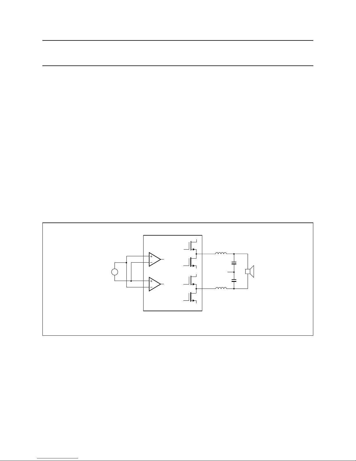
8.4 Differential audio inputs
For a high common mode rejection ratio and a maximum
of flexibility in the application, the audio inputs are fully
differential. By connecting the inputs anti-parallel the
phase of one of the channels can be inverted, so that a
load can be connected between the two output filters.
In this case the system operates as a mono BTL amplifier
and with the same loudspeaker impedance an
approximately four times higher output power can be
obtained.
The input configuration for a mono BTL application is
illustrated in Fig.6; for more information see Chapter 16.
In the stereo single-ended configuration it is also
recommended to connect the two differential inputs in
anti-phase. This has advantages for the current handling
of the power supply at low signal frequencies.
handbook, full pagewidth
V
in
IN1+
OUT1
power stage
MBL466
OUT2
SGND
IN1−
IN2+
IN2−
Fig.6 Input configuration for mono BTL application.
Page 11

2003 Mar 20 11
Philips Semiconductors Objective specification
2 × 25 W class-D power amplifier TDA8922
9 LIMITING VALUES
In accordance with the Absolute Maximum Rating System (IEC 60134).
Notes
1. See Section 16.6.
10 THERMAL CHARACTERISTICS
Note
1. See Section 16.5.
11 QUALITY SPECIFICATION
In accordance with
“General Quality Specification for Integrated Circuits: SNW-FQ-611D”
if this device is used as an
audio amplifier.
SYMBOL PARAMETER CONDITIONS MIN. MAX. UNIT
V
P
supply voltage −±30 V
V
MODE
input voltage on pin MODE with respect to SGND − 5.5 V
V
sc
short-circuit voltage on output pins −±30 V
I
ORM
repetitive peak current in output pin note 1 − 4A
T
stg
storage temperature −55 +150 °C
T
amb
ambient temperature −40 +85 °C
T
vj
virtual junction temperature − 150 °C
SYMBOL PARAMETER CONDITIONS VALUE UNIT
R
th(j-a)
thermal resistance from junction to ambient in free air; note 1
TDA8922TH 35 K/W
TDA8922J 35 K/W
R
th(j-c)
thermal resistance from junction to case note 1
TDA8922TH 1.3 K/W
TDA8922J 1.3 K/W
Page 12

2003 Mar 20 12
Philips Semiconductors Objective specification
2 × 25 W class-D power amplifier TDA8922
12 STATIC CHARACTERISTICS
VP= ±25 V; T
amb
=25°C; measured in Fig.10; unless otherwise specified.
Notes
1. The circuit is DC adjusted at V
P
= ±12.5 to ±30 V.
2. With respect to SGND (0 V).
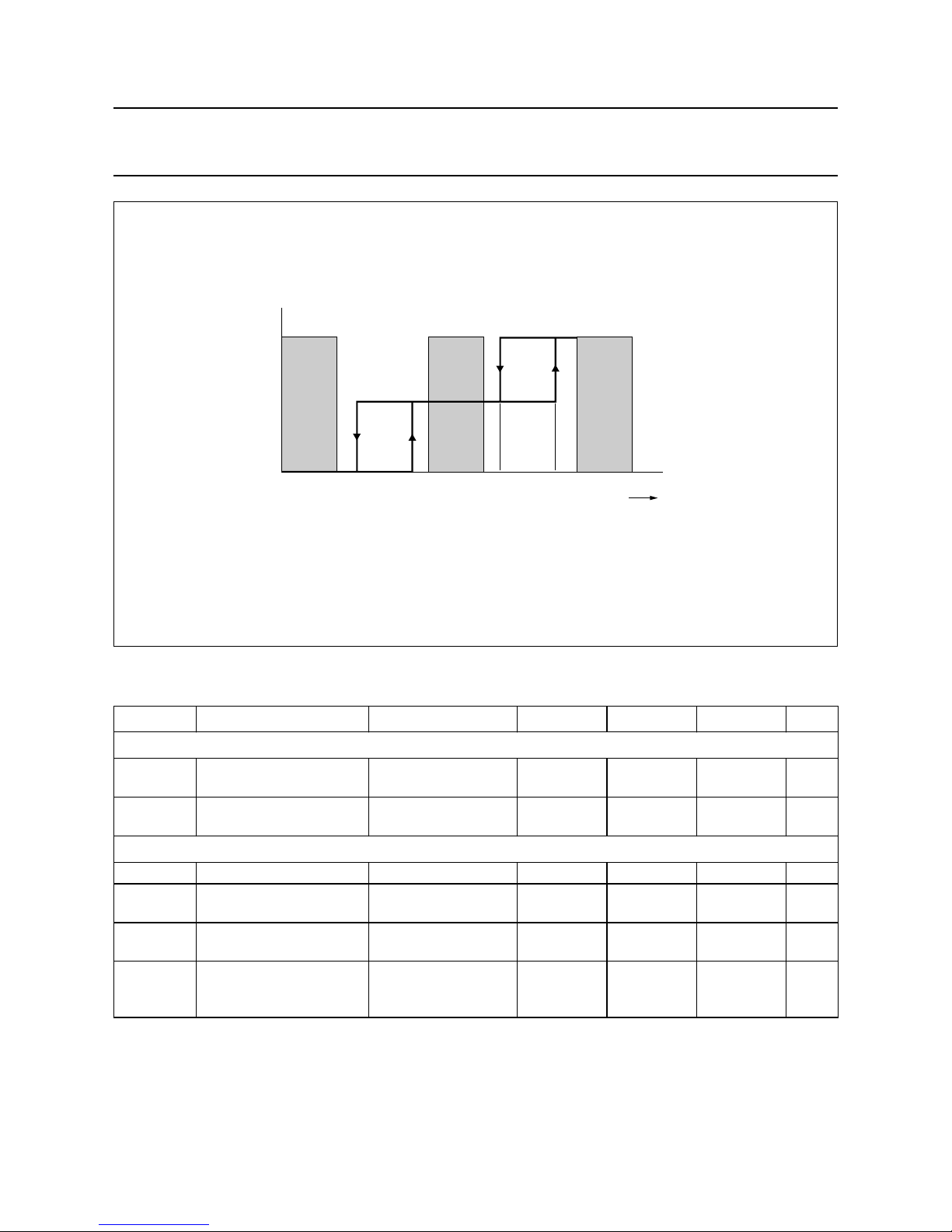
3. The transition regions between standby, mute and operating mode contain hysteresis (see Fig.7).
4. With respect to V
SSP1
.
SYMBOL PARAMETER CONDITIONS MIN. TYP. MAX. UNIT
Supply
V
P
supply voltage note 1 ±12.5 ±20 ±30 V
I
q(tot)
total quiescent supply current no load connected − 55 75 mA
I
stb
standby supply current − 100 500 µA
Mode select input; pin MODE
V
MODE
input voltage note 2 0 − 5.5 V
I
MODE
input current V
MODE
= 5.5 V −−1000 µA
V
stb
input voltage for standby mode notes2 and 3 0 − 0.8 V
V
mute
input voltage for mute mode notes 2 and 3 2.2 − 3.0 V
V
on
input voltage for operating mode notes 2 and 3 4.2 − 5.5 V
Audio inputs; pins IN1−, IN1+, IN2+ and IN2−
V
I
DC input voltage note 2 − 0 − V
Amplifier outputs; pins OUT1 and OUT2
V
OO(SE)
output offset voltage SE; operating and mute −−150 mV
∆V
OO(SE)
variation of output offset voltage SE; operating ↔ mute −−80 mV
V
OO(BTL)
output offset voltage BTL; operating and mute −−215 mV
∆V
OO(BTL)
variation of output offset voltage BTL; operating ↔ mute −−115 mV
Stabilizer output; pin STABI
V
o(stab)
stabilizer output voltage mute and operating; note 4 11 13 15 V
Temperature protection
T
prot
temperature protection activation 150 −−°C
T
hys
hysteresis on temperature
protection
− 20 −°C
Page 13
2003 Mar 20 13
Philips Semiconductors Objective specification
2 × 25 W class-D power amplifier TDA8922
handbook, full pagewidth
STBY MUTE ON
5.5
MBL467
V
MODE
(V)
4.23.02.20.80
Fig.7 Behaviour of mode selection pin MODE.
13 SWITCHING CHARACTERISTICS
VDD= ±25 V; T
amb
=25°C; measured in Fig.10; unless otherwise specified.
Note
1. Frequency set with R
OSC
according to the formula in Section 8.2.
SYMBOL PARAMETER CONDITIONS MIN. TYP. MAX. UNIT
Internal oscillator
f
osc
typical internal oscillator
frequency
R
OSC
= 30.0 kΩ 290 317 344 kHz
f
osc(int)
internal oscillator
frequency range
note 1 210 − 600 kHz
External oscillator or frequency tracking
V
OSC
voltage on pin OSC SGND + 4.5 SGND+ 5 SGND + 6 V
V
OSC(trip)
trip level for tracking on
pin OSC
− SGND + 2.5 − V
f
track
frequency range for
tracking
210 − 600 kHz
V
P(OSC)(ext)
minimum symmetrical
supply voltage forexternal
oscillator application
15 −−V
Page 14

2003 Mar 20 14
Philips Semiconductors Objective specification
2 × 25 W class-D power amplifier TDA8922
14 DYNAMIC AC CHARACTERISTICS (STEREO AND DUAL SE APPLICATION)
VP= ±20 V; RL=8Ω; fi= 1 kHz; f
osc
= 310 kHz; RsL< 0.1 Ω (note 1); T
amb
=25°C; measured in Fig.10; unless
otherwise specified.
Notes
1. R
sL
is the series resistance of inductor of low-pass LC filter in the application.
2. Output power is measured indirectly; based on R
DSon
measurement.
3. Total harmonic distortion is measured in a bandwidth of 22 Hz to 22 kHz. When distortion is measured using a lower
order low-pass filter a significantly higher value is found, due to the switching frequency outside the audio band.
Maximum limit is guaranteed but may not be 100% tested.
4. Output power measured across the loudspeaker load.
5. V
ripple=Vripple(max)
= 2 V (p-p); Rs=0Ω.
6. B = 22 Hz to 22 kHz; Rs=0Ω; maximum limit is guaranteed, but may not be 100% tested.
7. B = 22 Hz to 22 kHz; Rs=10kΩ.
SYMBOL PARAMETER CONDITIONS MIN. TYP. MAX. UNIT
P
o
output power RL=8Ω; VP= ±20 V; note 2
THD = 0.5% 18 20 − W
THD = 10% 22 25 − W
R
L
=8Ω; VP= ±25 V; note 2
THD = 0.5% 29 33 − W
THD = 10% 36 40 − W
R
L
=4Ω; VP= ±15 V; note 2
THD = 0.5% 18 20 − W
THD = 10% 22 25 − W
THD total harmonic distortion P
o
= 1 W; note 3
f
i
= 1 kHz − 0.02 0.05 %
f
i
= 10 kHz − 0.15 − %
G
v(cl)
closed loop voltage gain 29 30 31 dB
η efficiency P
o
= 25 W; fi= 1 kHz; note 4 85 90 − %
SVRR supply voltage ripple rejection operating; note 5
f
i
= 100 Hz − 55 − dB
f
i
= 1 kHz 40 50 − dB
mute; f
i
= 100 Hz; note 5 − 55 − dB
standby; f
i
= 100 Hz; note 5 − 80 − dB
Z
i
input impedance 45 68 − kΩ
V
n(o)
noise output voltage operating
R
s
=0Ω; note 6 − 200 400 µV
R
s
=10kΩ; note 7 − 230 −µV
mute; note 8 − 220 −µV
αcschannel separation note 9 − 70 − dB
∆G
v
channel unbalance −−1dB
V
o(mute)
output signal in mute note 10 −−400 µV
CMRR common mode rejection ratio V
i(CM)
= 1 V (RMS) − 75 − dB
Page 15

2003 Mar 20 15
Philips Semiconductors Objective specification
2 × 25 W class-D power amplifier TDA8922
8. B = 22 Hz to 22 kHz; independent of Rs.
9. Po= 1 W; Rs=0Ω; fi= 1 kHz.
10. Vi=V
i(max)
= 1 V (RMS); maximum limit is guaranteed, but may not be 100% tested.
15 DYNAMIC AC CHARACTERISTICS (MONO BTL APPLICATION)
VP= ±15 V; RL=8Ω; fi= 1 kHz; f
osc
= 310 kHz; RsL< 0.1 Ω (note 1); T
amb
=25°C; measured in Fig.10; unless
otherwise specified.
Notes
1. R
sL
is the series resistance of inductor of low-pass LC filter in the application.
2. Output power is measured indirectly; based on R
DSon
measurement.
3. Total harmonic distortion is measured in a bandwidth of 22 Hz to 22 kHz. When distortion is measured using a low
order low-pass filter a significant higher value will be found, due to the switching frequency outside the audio band.
Maximum limit is guaranteed but may not be 100% tested.
4. Output power measured across the loudspeaker load.
5. V
ripple=Vripple(max)
= 2 V (p-p); Rs=0Ω.
6. B = 22 Hz to 22 kHz; Rs=0Ω; maximum limit is guaranteed, but may not be 100% tested.
7. B = 22 Hz to 22 kHz; Rs=10kΩ.
8. B = 22 Hz to 22 kHz; independent of Rs.
9. Vi=V
i(max)
= 1 V (RMS); fi= 1 kHz; maximum limit is guaranteed, but may not be 100% tested.
SYMBOL PARAMETER CONDITIONS MIN. TYP. MAX. UNIT
P
o
output power RL=8Ω; VP= ±15 V; note 2
THD = 0.5% 37 40 − W
THD = 10% 46 50 − W
THD total harmonic distortion P
o
= 1 W; note 3
f
i
= 1 kHz − 0.015 0.05 %
f
i
= 10 kHz − 0.02 − %
G
v(cl)
closed loop voltage gain 35 36 37 dB
η efficiency P
o
= 50 W; fi= 1 kHz; note 4 85 90 − %
SVRR supply voltage ripple rejection operating; note 5
fi= 100 Hz − 49 − dB
f
i
= 1 kHz 36 44 − dB
mute; f
i
= 100 Hz; note 5 − 49 − dB
standby; f
i
= 100 Hz; note 5 − 80 − dB
Z
i
input impedance 22 34 − kΩ
V
n(o)
noise output voltage operating
R
s
=0Ω; note 6 − 280 560 µV
R
s
=10kΩ; note 7 − 300 −µV
mute; note 8 − 280 −µV
V
o(mute)
output signal in mute note 9 −−500 µV
CMRR common mode rejection ratio V
i(CM)
= 1 V (RMS) − 75 − dB
Page 16
2003 Mar 20 16
Philips Semiconductors Objective specification
2 × 25 W class-D power amplifier TDA8922
16 APPLICATION INFORMATION
16.1 BTL application
When using the power amplifier in a monoBTL application
(for more output power), the inputs of both channels must
be connected in parallel and the phase of one of the inputs
must be inverted (see Fig.6). In principle the loudspeaker
can be connected between the outputs of the two
single-ended demodulation filters.
16.2 Pin MODE
For correct operation the switching voltage at pin MODE
should be debounced. If pin MODE is driven by a
mechanical switch an appropriate debouncing low-pass
filter should be used. If pin MODE is driven by an
electroniccircuit or microcontroller then itshould remain at
the mute voltage level for at least 100 ms before switching
back to the standby voltage level.
16.3 Output power estimation
The output power in several applications (SE and BTL)
can be estimated using the following expressions:
SE:
Maximum current:
should not exceed 4 A.
BTL:
Maximum current:
should not exceed 4 A.
Legend:
R
L
= load impedance
f
osc
= oscillator frequency
t
min
= minimum pulse width (typical 190 ns)
VP= single-sided supply voltage (so, if supply is ±30 V
symmetrical, then VP=30V)
P
o(1%)
= output power just at clipping
P
o(10%)
= output power at THD = 10%
P
o(10%)
= 1.25 × P
o(1%)
.
16.4 External clock
The minimum required symmetrical supply voltage for
external clock application is ±15 V (equally, the minimum
asymmetrical supply voltage for applications with an
external clock is 30 V).
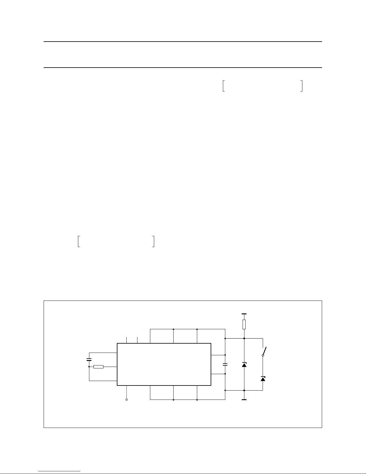
Whenusing an external clock the following accuracyof the
duty cycle of the external clock has to be taken into
account: 47.5% < δ < 52.5%.
A possible solution for an external clock oscillator circuit is
illustrated in Fig.8.
P
o(1%)
R
L
RL0.6+
---------------------
V
P
1t
minfosc
×–()××
2
2R
L
×
----------------------------------------------------------------------------------------- -
=
I
o(peak)
VP1t
minfosc
×–()×
R
L
0.6+
-----------------------------------------------------
=
P
o(1%)
R
L
RL1.2+
---------------------
2V
P
1t
minfosc
×–()××
2
2R
L
×
---------------------------------------------------------------------------------------------
=
I
o(peak)
2VP1t
minfosc
×–()×
R
L
1.2+
-------------------------------------------------------- -
=
handbook, full pagewidth
1
14
7
2
111310 4 5 6
8912
3
CTC
0−
0+
ASTAB− ASTAB+ −TRIGGER
+TRIGGER RETRIGGERMR
220
nF
5.6 V
4.3 V
HOP
GND
MBL468
HEF4047BT
V
DD
360 kHz 320 kHz
V
DDA
V
SS
9.1 kΩ
2 kΩ
120 pF
RTC
CLOCK
RCTC
Fig.8 External oscillator circuit.
Page 17
2003 Mar 20 17
Philips Semiconductors Objective specification
2 × 25 W class-D power amplifier TDA8922
16.5 Heatsink requirements
In some applications it may be necessary to connect an
external heatsink to the TDA8922. The determining factor
is the 150 °C maximum junction temperature T
j(max)
which
cannot be exceeded. The expression below shows the
relationship between the maximum allowable power
dissipation and the total thermal resistance from junction
to ambient:
P
diss
is determined by the efficiency (η) of the TDA8922.
The efficiency measured in the TDA8922 as a function of
output power is given in Fig.19. The power dissipation can
be derived as function of output power (see Fig.18).
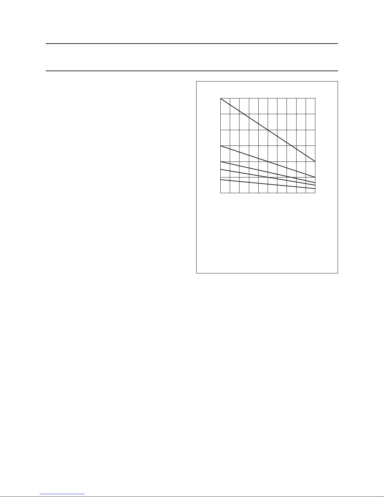
Thederatingcurves(given for several values of the R
th(j-a)
)
are illustrated in Fig.9. A maximum junction temperature
Tj= 150 °Cistakeninto account. From Fig.9 the maximum
allowable power dissipation for a given heatsink size can
bederivedortherequiredheatsinksizecanbedetermined
at a required dissipation level.
Example 1:
Po=2×25 W into 8 Ω
T
j(max)
= 150 °C
T
amb
=60°C
P
diss(tot)
= 4.2 W (from Fig.18)
The required R
th(j-a)
= 21.4 K/W can be calculated.
The R
th(j-a)
of the TDA8922 in free air is 35 K/W; the R
th(j-c)
of the TDA8922 is 1.3 K/W, thus a heatsink of 20.1 K/W is
required for this example.
In actual applications, other factors such as the average
power dissipation with music source (as opposed to a
continuous sine wave) will determine the size of the
heatsink required.
Example 2:
Po=2×25 W into 4 Ω
T
j(max)
= 150 °C
T
amb
=60°C
P
diss(tot)
= 5.5 W (from Fig.18)
The required R
th(j-a)
= 16.4 K/W.
The R
th(j-a)
of the TDA8922 in free air is 35 K/W; the R
th(j-c)
of the TDA8922 is 1.3 K/W, thus a heatsink of 15.1 K/W is
required for this example.
16.6 Output current limiting
To guarantee the robustness of the class-D amplifier the
maximum output current which can be delivered by the
output stage is limited. An overcurrent protection is
included for each output power switch. When the current
flowing through any of the power switches exceeds a
defined internal threshold (e.g. in case of a short-circuit to
the supply lines or a short-circuit across the load), the
amplifier will shut down immediately and an internal timer
willbestarted. After a fixed time (e.g. 100 ms) theamplifier
is switched on again. If the requested output current is still
too high the amplifier will switch-off again. Thus the
amplifier will try to switch to the operating mode every
100 ms. The average dissipation will be low in this
situation because of this low duty cycle. If the overcurrent
condition is removed the amplifier will remain operating.
Becausethe duty cycle is low theamplifier will be switched
off for a relatively long period of time which will be noticed
as a so-called audio-hole; an audible interruption in the
output signal.
R
th(j-a)
T
j(max)Tamb
–
P
diss
-----------------------------------
=
handbook, halfpage
0
P
diss
(W)
30
20
10
0
20 100
T
amb
(°C)
40
(1)
(2)
(3)
(4)
(5)
60 80
MBL469
Fig.9 Derating curves for power dissipation as a
function of maximum ambient temperature.
(1) R
th(j-a)
= 5 K/W.
(2) R
th(j-a)
= 10 K/W.
(3) R
th(j-a)
= 15 K/W.
(4) R
th(j-a)
= 20 K/W.
(5) R
th(j-a)
= 35 K/W.
Page 18

2003 Mar 20 18
Philips Semiconductors Objective specification
2 × 25 W class-D power amplifier TDA8922
To trigger the maximum current protection in the
TDA8922, the required output current must exceed 4 A.
This situation occurs in case of:
• Short-circuits from any output terminal to the supply
lines (VDD or VSS)
• Short-circuit across the load or speaker impedances or
a load impedance below the specified values of
4 and 8 Ω.
Even if load impedances are connected to the amplifier
outputs which have an impedance rating of 4 Ω, this
impedance can be lower due to the frequency
characteristic of the loudspeaker; practical loudspeaker
impedances can be modelled as an RLC network which
will have a specific frequency characteristic: the
impedance at the output of the amplifier will vary with the
input frequency. A high supply voltage in combination with
a low impedance will result in large current requirements.
Another factor which must be taken into account is the
ripplecurrent which will also flow through the output power
switches. This ripple current depends on the inductor
values which are used, supply voltage, oscillator
frequency, duty factor and minimum pulse width. The
maximum available output current to drive the load
impedance can be calculated by subtracting the ripple
current from the maximum repetitive peak current in the
output pin, which is 4 A for the TDA8922.
As a rule of thumb the following expressions can be used
to determine the minimum allowed load impedance
without generating audio holes:
for SE application.
for BTL application.
Where:
ZL= load impedance
f
osc
= oscillator frequency
t
min
= minimum pulse width (typical 190 ns)
VP= single-sided supply voltage
(so, if the supply is ±30 V symmetrical, then VP=30V)
I
ORM
= maximum repetitive peak current in output pin;
see also Chapter 9
I
ripple
= ripple current.
See the application notes (tbf) for a more detailed
description of the implications of output current limiting.
16.7 Pumping effects
The TDA8922 class-D amplifier is supplied by a
symmetrical voltage (e.g VDD= +25 V and VSS= −25 V).
When the amplifier is used in a SE configuration, a
so-called ‘pumping effect’ can occur. During one switching
interval, energy is taken from one supply (e.g. VDD), while
a part of that energy is delivered back to the other supply
line (e.g. VSS) and visa versa. When the voltage supply
source cannot sink energy, the voltage across the output
capacitors of that voltage supply source will increase:
the supply voltage is pumped to higher levels. The voltage
increase caused by the pumping effect depends on:
• Speaker impedance
• Supply voltage
• Audio signal frequency
• Capacitor value present on supply lines
• Source and sink currents of other channels.
The pumping effect should not cause a malfunction of
eithertheaudioamplifierand/orthe voltage supply source.
For instance, this malfunction can be caused by triggering
oftheundervoltageorovervoltageprotectionorunbalance
protection of the amplifier.
See the application notes (tbf) for a more detailed
description of the implications of output current limiting.
16.8 Reference design
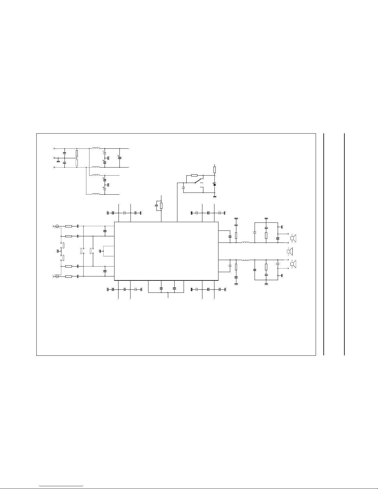
The reference design for a single-chip class-D audio
amplifier using the TDA8922TH is illustrated in Fig.10.
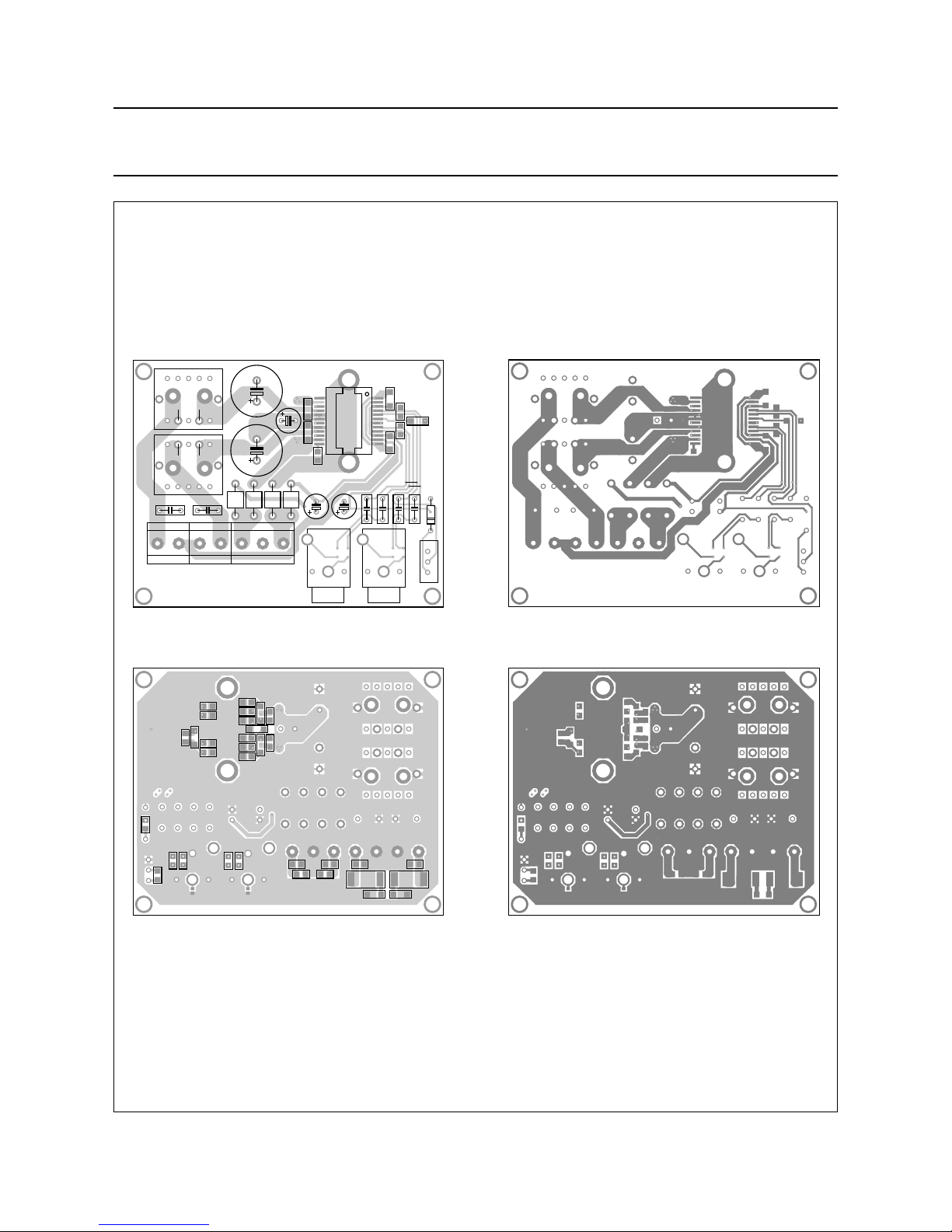
The Printed-CircuitBoard (PCB) layout is shown in Fig.11.
The Bill Of Materials (BOM) is given in Table 1.
16.9 PCB information for HSOP24 package
The size of the PCB is 74.3 × 59.10 mm, dual sided 35 µm
copper with 121 metallized through holes.
The standard configuration has a symmetrical supply
(typical ±20 V) with stereo SE outputs (typical 2 × 8 Ω).
The PCB is also suitable for a mono BTL configuration
(1 × 8 Ω) with symmetrical and asymmetrical supply.
It is possible to use several different output filter inductors
such as 16RHBP or EP13 types to evaluate the
performance against the price or size.
16.10 Classification
The application shows optimized signal and EMI
performance.
Z
L
VP1t
minfosc
×–()×
I
ORMIripple
–
-----------------------------------------------------
0.6–≥
Z
L
2VP1t
minfosc
×–()×
I
ORMIripple
–
---------------------------------------------------------
1.2–≥
Page 19
2003 Mar 20 19
Philips Semiconductors Objective specification
2 × 25 W class-D power amplifier TDA8922
This text is here in white to force landscape pages to be rotated correctly when browsing through the pdf in the Acrobat reader.This text is here in
_white to force landscape pages to be rotated correctly when browsing through the pdf in the Acrobat reader.This text is here inThis text is here in
white to force landscape pages to be rotated correctly when browsing through the pdf in the Acrobat reader. white to force landscape pages to be ...
a
gewidth
MGU997
TDA8922TH
C20
330 pF
C10
100 nF
C12
100 nF
C11
220 nF
C9
220 nF
C8
220 nF
on
mute
off
R5
30 kΩ
C17
470 nF
R7
5.6 kΩ
C16
470 nF
R6
5.6 kΩ
J4
(1)
J3
C21
330 pF
8
10 12 7 6
1 3 24 18 13 19 23 20
V
DDA1VSSA1
OSC MODE
V
DDAVSSA
V
SSA
9
11
2
5
15
OUT1
BOOT1
BOOT2
OUT2
16
21
22
4
IN1
+
IN1
−
IN2
+
IN2
−
SGND1
SGND
C13
100 nF
C14
220 nF
C15
100 nF
14 17
V
DDP1VSSP1
V
DDP
V
DDA
V
SSP
R4 39 kΩ
R3
39 kΩ
Z1
5.6 V
S1
C34
100 nF
C35
220 nF
C36
100 nF
C32
220 nF
C33
47 pF
V
SSA2VDDA2VSSD
STABI PROT HW
V
SSAVDDA
V
SSP
C37
100 nF
C38
220 nF
C39
100 nF
C22
15 nF
C23
15 nF
C30
15 nF
C31
15 nF
C26
470 nF
C27
470 nF
R10
4.7 Ω
C24
560 pF
R11
4.7 Ω
C25
560 pF
R12
22 Ω
R13
22 Ω
C28
220 nF
C29
220 nF
L5
27 µH
L6
27 µH
V
DDP2VSSP2
V
DDP
SGND
SE 4 Ω
SE 4 Ω
OUT1
−
OUT1
+
OUT2
−
OUT2
+
V
SSP
SGND2
J2
(4)
J1
in 1
in 2
C18
470 nF
R8
5.6 kΩ
C19
470 nF
R9
5.6 kΩ
(2)
BTL 8 Ω
L1
BEAD
L2
BEAD
C1
470 µF
C3
47 µF
C2
470 µF
C6
100 nF
C7
100 nF
V
DDP
V
SSP
R1
(3)
10 kΩ
R2
(3)
9.1 kΩ
V
DDA
V
SSA
C4
47 µF
C5
47 µF
GND
V
SS
V
DD
L3
BEAD
L4
BEAD
+
25 V
−
25 V
SGND
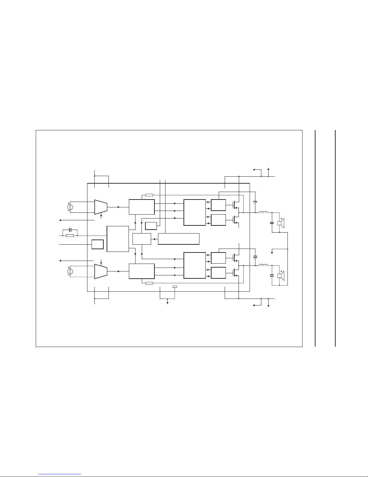
Fig.10 Single-chip class-D audio amplifier application diagram (reference design for SE and BTL).
(1) BTL: remove In2, R8, R9, C18, C19, C21 and close J3 and J4.
(2) BTL: connect loudspeaker between OUT1+ and OUT2−.
(3) BTL: R1 and R2 are only required when an asymmetrical supply is used (VSS= 0 V).
(4) In case of hum, close J1 and J2.
Every decoupling to ground (plane) must be made as close as possible to the pin.
To handle 20 Hz under all conditions in stereo SE mode, the external power supply
needs to have a capacitance of at least 4700 µF per supply line; V
P
= ±27 V (max).
Page 20
2003 Mar 20 20
Philips Semiconductors Objective specification
2 × 25 W class-D power amplifier TDA8922
handbook, full pagewidth
−
Out1
+
V
SS
In1 In2
S1
Z1
C19
C18C16C17
C26C27
C4
C1
U1
1-2002PCB version 4
J4
J3
C3
C38
C14
C33
C29
R13R12
C28
R1R2
R5
R11
R10
R6R7
R9R8
R4
R3
J1J2
C6C7
C34
C25
C24
C23
C22
C9
C12
C36
C37
C39
C15
C32
C13
C10
C31C30
C35
C21
C20
C8
C11
C2
C5
L3 L2 L4
L5
L6
L1
On
Off
TDA8920/21/22/23/24TH
state of D art
PHILIPS SEMICONDUCTORS
VDDGND
−
Out2
+
MBL496
Top copperTop silk screen
Bottom copperBottom silk screen
Fig.11 Printed-circuit board layout for the TDA8922TH.
Page 21

2003 Mar 20 21
Philips Semiconductors Objective specification
2 × 25 W class-D power amplifier TDA8922
16.11 Bill of materials for reference design
Table 1 Single-chip class-D audio amplifier printed-circuit board (PCB version 4; 1-2002) for TDA8922TH
(see Figs 10 and 11).
BOM ITEM QUANTITY REFERENCE PART DESCRIPTION
1 1 U1 TDA8922TH Philips Semiconductors B.V.
2 2 in1 and in2 cinch inputs Farnell 152-396
3 2 out1 and out2 output connector Augat 5KEV-02
41V
DD
, GND and V
SS
supply connector Augat 5KEV-03
5 2 L6 and L5 27 µH EP13 or 16RHBP
6 4 L1, L2, L3 and L4 BEAD Murata BL01RN1-A62
7 1 S1 PCB switch Knitter ATE1E M-O-M
8 1 Z1 5V6 BZX 79C5V6 DO-35
9 2 C1 and C2 470 µF; 35 V Panasonic M series
ECA1VM471
10 3 C3, C4 and C5 47 µF; 63 V Panasonic NHG series
ECA1JHG470
11 6 C16, C17, C18, C19, C26 and
C27
470 nF; 63 V MKT EPCOS B32529-C474-K
12 9 C8, C9, C11, C14, C28, C29,
C32, C35 and C38
220 nF; 63 V SMD 1206
13 10 C6, C7, C10, C12, C13, C15,
C34, C36, C37 and C39
100 nF; 50 V SMD 0805
14 2 C20 and C21 330 pF; 50 V SMD 0805
15 4 C22, C23, C30 and C31 15 nF; 50 V SMD 0805
16 2 C24, C25 560 pF; 100 V SMD 0805
17 1 C33 47 pF; 25V SMD 0805
18 2 R4 and R3 39 kΩ; 0.1 W SMD 0805
19 1 R5 30 kΩ; 0.1 W SMD 1206
20 1 R1 10 kΩ; 0.1 W; optional SMD 0805
21 1 R2 9.1 kΩ; 0.1 W; optional SMD 0805
22 4 R6, R7, R8 and R9 5.6 kΩ; 0.1 W SMD 0805
23 2 R13 and R12 22 Ω; 1 W SMD 2512
24 2 R10 and R11 4.7 Ω; 0.25 W SMD 1206
25 2 J1 and J2 solder dot jumpers for ground reference in case of hum
(60 Hz noise)
26 2 J3 and J4 wire jumpers for BTL application
27 1 heatsink 30 mm SK400; OK for maximum music dissipation;
1/8 Prated (2 × 75 W/8) in 2 × 4 Ω at T
amb
=70°C
28 1 printed-circuit board material 1.6 mm thick epoxy FR4 material, double sided 35 µm
copper; clearances 300 µm; minimum copper track
400 µm
Page 22
2003 Mar 20 22
Philips Semiconductors Objective specification
2 × 25 W class-D power amplifier TDA8922
16.12 Curves measured in reference design
Thecurvesillustrated in Figs 20 and 21 are measured with
a specified load impedance. Spread in ZL(e.g. due to the
frequency characteristics of the loudspeaker) can trigger
the maximum current protection circuit; see Section 16.6.
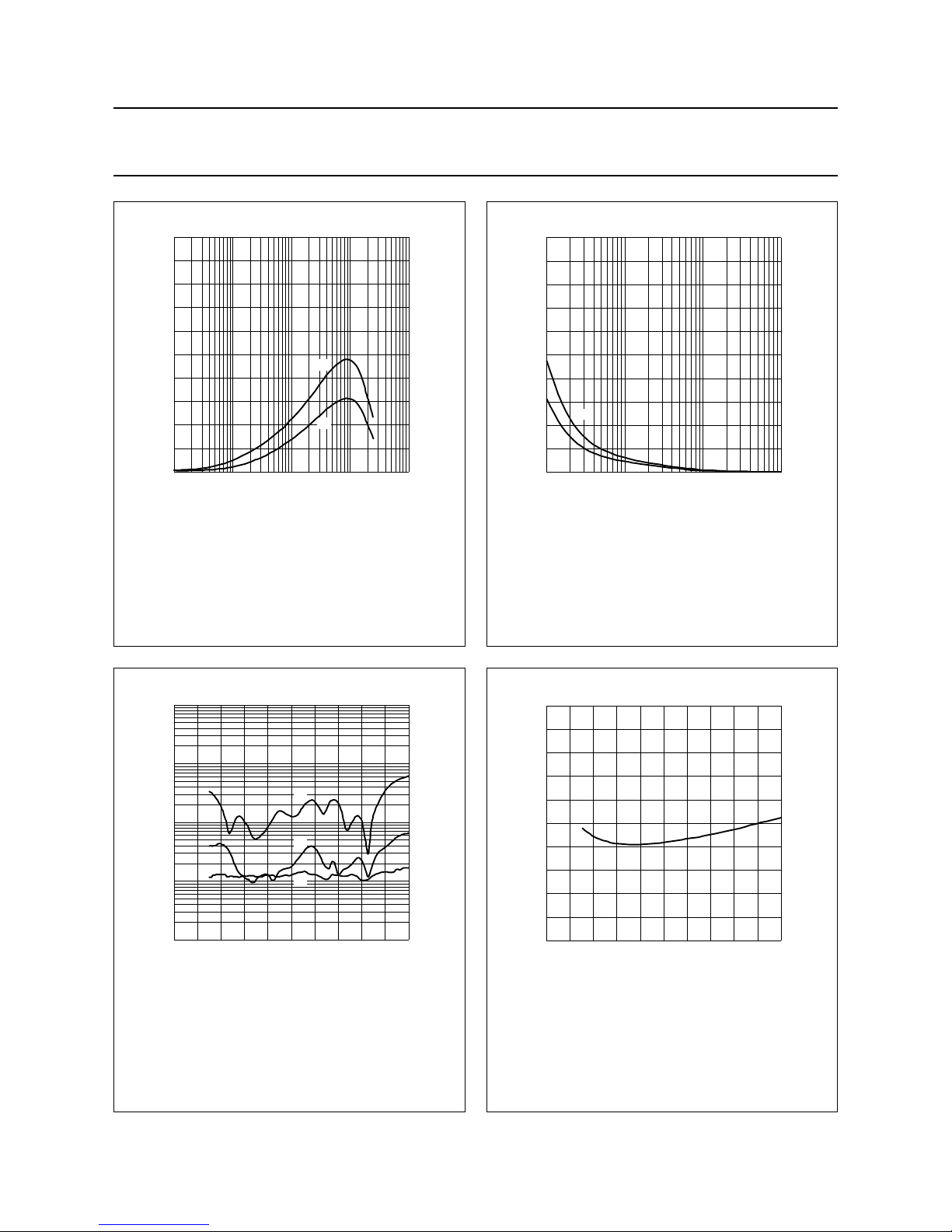
The curves illustrated in Figs 30 and 31 show the effects
of supply pumping when only one single-ended channel is
driven with a low frequency signal; see Section 16.7.
handbook, halfpage
MGX324
Po (W)
10
−2
10
−1
11010
2
THD + N
(%)
10
2
10
1
10
−1
10
−2
10
−3
(1)
(2)
(3)
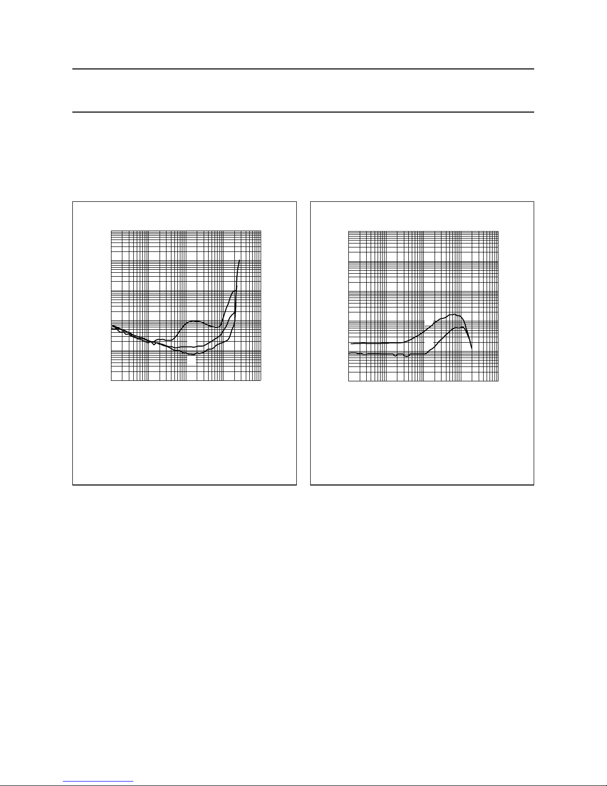
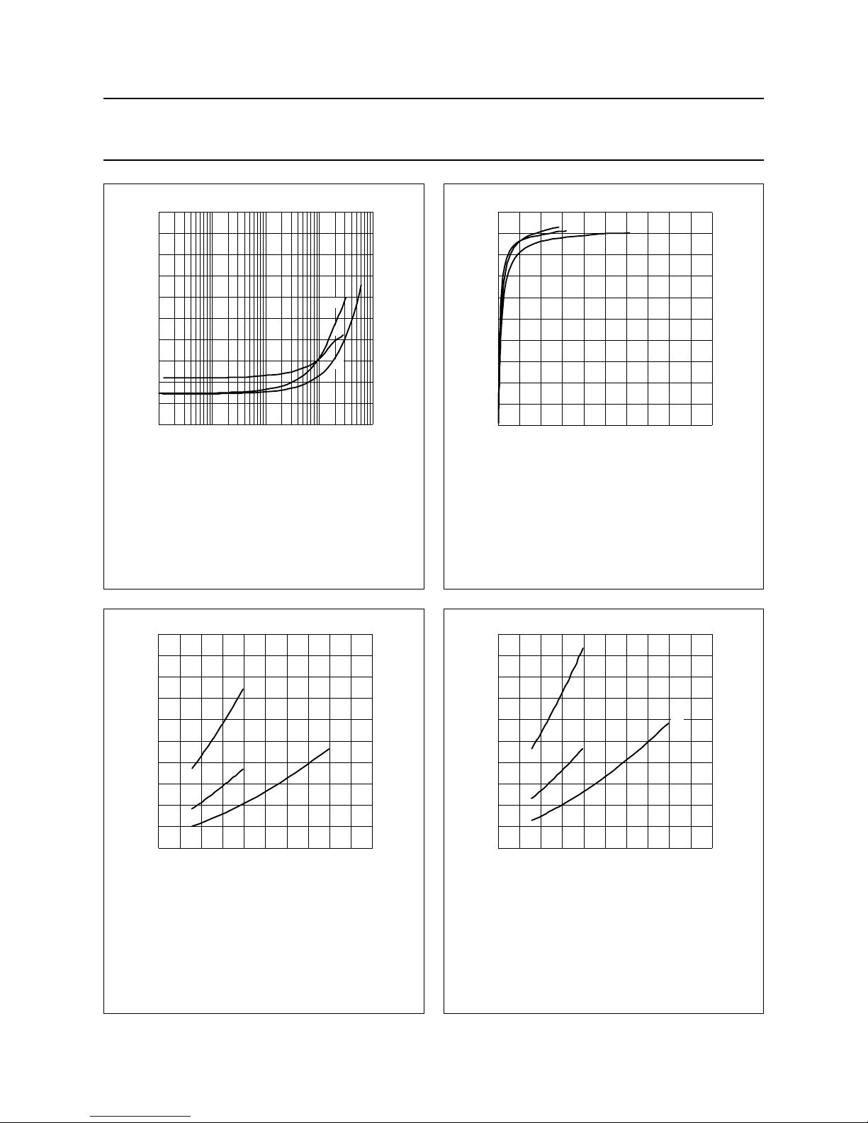
Fig.12 THD + N as a function of output power.
2 × 8 Ω SE; VP= ±20 V.
(1) 10 kHz.
(2) 1 kHz.
(3) 100 Hz.
handbook, halfpage
MGX327
fi (Hz)
10 10
2
10
3
10
4
10
5
THD + N
(%)
10
2
10
1
10
−1
10
−2
10
−3
(1)
(2)
Fig.13 THD + N as a function of input frequency.
2 × 8 Ω SE; VP= ±20 V.
(1) Po=10W.
(2) Po=1W.
Page 23
2003 Mar 20 23
Philips Semiconductors Objective specification
2 × 25 W class-D power amplifier TDA8922
handbook, halfpage
MGX325
Po (W)
10
−2
10
−1
11010
2
THD + N
(%)
10
2
10
1
10
−1
10
−2
10
−3
(1)
(2)
(3)
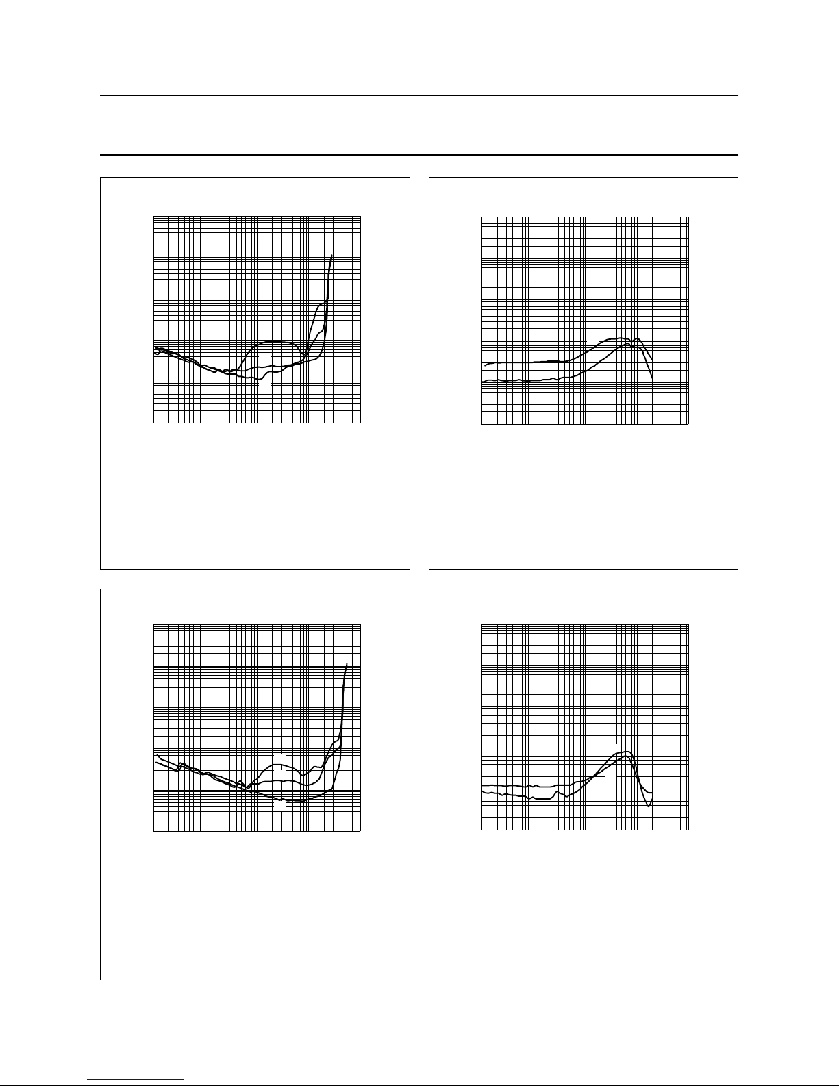
Fig.14 THD + N as a function of output power.
2 × 4 Ω SE; VP= ±15 V.
(1) 10 kHz.
(2) 1 kHz.
(3) 100 Hz.
handbook, halfpage
MGX328
fi (Hz)
10 10
2
10
3
10
4
10
5
THD + N
(%)
10
2
10
1
10
−1
10
−2
10
−3
(1)
(2)
Fig.15 THD + N as a function of input frequency.
2 × 4 Ω SE; VP= ±15 V.
(1) Po=10W.
(2) Po=1W.
handbook, halfpage
MGX326
Po (W)
10
−2
10
−1
11010
2
THD + N
(%)
10
2
10
1
10
−1
10
−2
10
−3
(1)
(2)
(3)
Fig.16 THD + N as a function of output power.
1 × 8 Ω BTL; VP= ±15 V.
(1) 10 kHz.
(2) 1 kHz.
(3) 100 Hz.
handbook, halfpage
MGX329
fi (Hz)
10 10
2
10
3
10
4
10
5
THD + N
(%)
10
2
10
1
10
−1
10
−2
10
−3
(1)
(2)
Fig.17 THD + N as a function of input frequency.
1 × 8 Ω BTL; VP= ±15 V.
(1) Po=10W.
(2) Po=1W.
Page 24
2003 Mar 20 24
Philips Semiconductors Objective specification
2 × 25 W class-D power amplifier TDA8922
handbook, halfpage
MGX332
P
diss
(W)
2
0
4
8
6
10
(1)
(2)
(3)
Po (W)
10
−2
10
−1
11010
2
Fig.18 Power dissipation as a function of output
power.
fi= 1 kHz.
(1) 2 × 4 Ω SE, VP= ±15 V.
(2) 2 × 8 Ω SE, VP= ±20 V.
(3) 1 × 8 Ω BTL, VP= ±15 V.
handbook, halfpage
η
(%)
06020 80 100
Po (W)
40
0
100
60
80
20
40
MGX333
(1)
(2)
(3)
Fig.19 Efficiency as a function of output power.
fi= 1 kHz.
(1) 2 × 8 Ω SE, VP= ±20 V.
(2) 2 × 4 Ω SE, VP= ±15 V.
(3) 1 × 8 Ω BTL, VP= ±15 V.
handbook, halfpage
P
o
(W)
10 2515 30 35
VDD (V)
20
0
100
60
80
20
40
MGX336
(1)
(2)
(3)
Fig.20 Output power as a function of supply
voltage.
THD+N=0.5%; fi= 1 kHz.
(1) 1 × 8 Ω BTL.
(2) 2 × 4 Ω SE.
(3) 2 × 8 Ω SE.
handbook, halfpage
P
o
(W)
10 2515 30 35
VDD (V)
20
0
100
60
80
20
40
MGX337
(1)
(2)
(3)
Fig.21 Output power as a function of supply
voltage.
THD + N = 10%; fi= 1 kHz.
(1) 1 × 8 Ω BTL.
(2) 2 × 4 Ω SE.
(3) 2 × 8 Ω SE.
Page 25
2003 Mar 20 25
Philips Semiconductors Objective specification
2 × 25 W class-D power amplifier TDA8922
handbook, halfpage
MGX330
α
cs
(dB)
−80
−100
−60
−20
−40
0
fi (Hz)
10 10
2
10
3
10
4
10
5
(2)
(1)
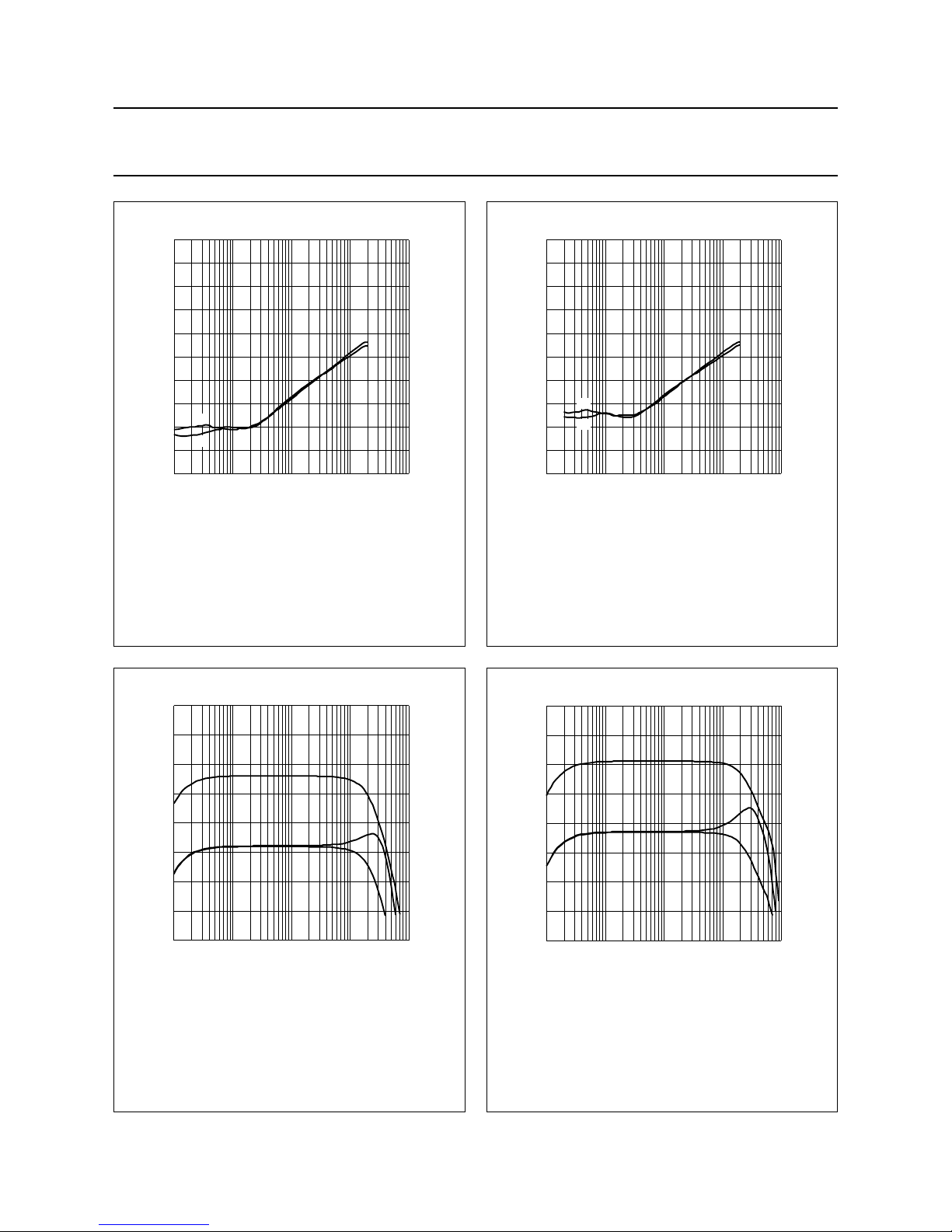
Fig.22 Channel separation as a function of input
frequency.
2 × 8 Ω SE; VP= ±20 V.
(1) Po=1W.
(2) Po=10W.
handbook, halfpage
MGX331
α
cs
(dB)
−80
−100
−60
−20
−40
0
fi (Hz)
10 10
2
10
3
10
4
10
5
(2)
(1)
Fig.23 Channel separation as a function of input
frequency.
2 × 4 Ω SE; VP= ±15 V.
(1) Po=1W.
(2) Po=10W.
handbook, halfpage
MGX340
G
(dB)
25
20
30
40
35
fi (Hz)
10 10
2
10
3
10
4
10
5
(1)
(2)
(3)
Fig.24 Gain as a function of input frequency.
Vi= 100 mV; Rs= 5.6 kΩ; Ci= 330 pF.
(1) 1 × 8 Ω BTL, VP= ±15 V.
(2) 2 × 8 Ω SE, VP= ±20 V.
(3) 2 × 4 Ω SE, VP= ±15 V.
handbook, halfpage
MGX341
G
(dB)
25
20
30
40
35
fi (Hz)
10 10
2
10
3
10
4
10
5
(1)
(2)
(3)
Fig.25 Gain as a function of input frequency.
Vi= 100 mV; Rs=0kΩ.
(1) 1 × 8 Ω BTL, VP= ±15 V.
(2) 2 × 8 Ω SE, VP= ±20 V.
(3) 2 × 4 Ω SE, VP= ±15 V.
Page 26
2003 Mar 20 26
Philips Semiconductors Objective specification
2 × 25 W class-D power amplifier TDA8922
handbook, halfpage
I
q
(mA)
0 5 10 2515 30 35
VDD (V)
20
0
100
60
80
20
40
MGX338
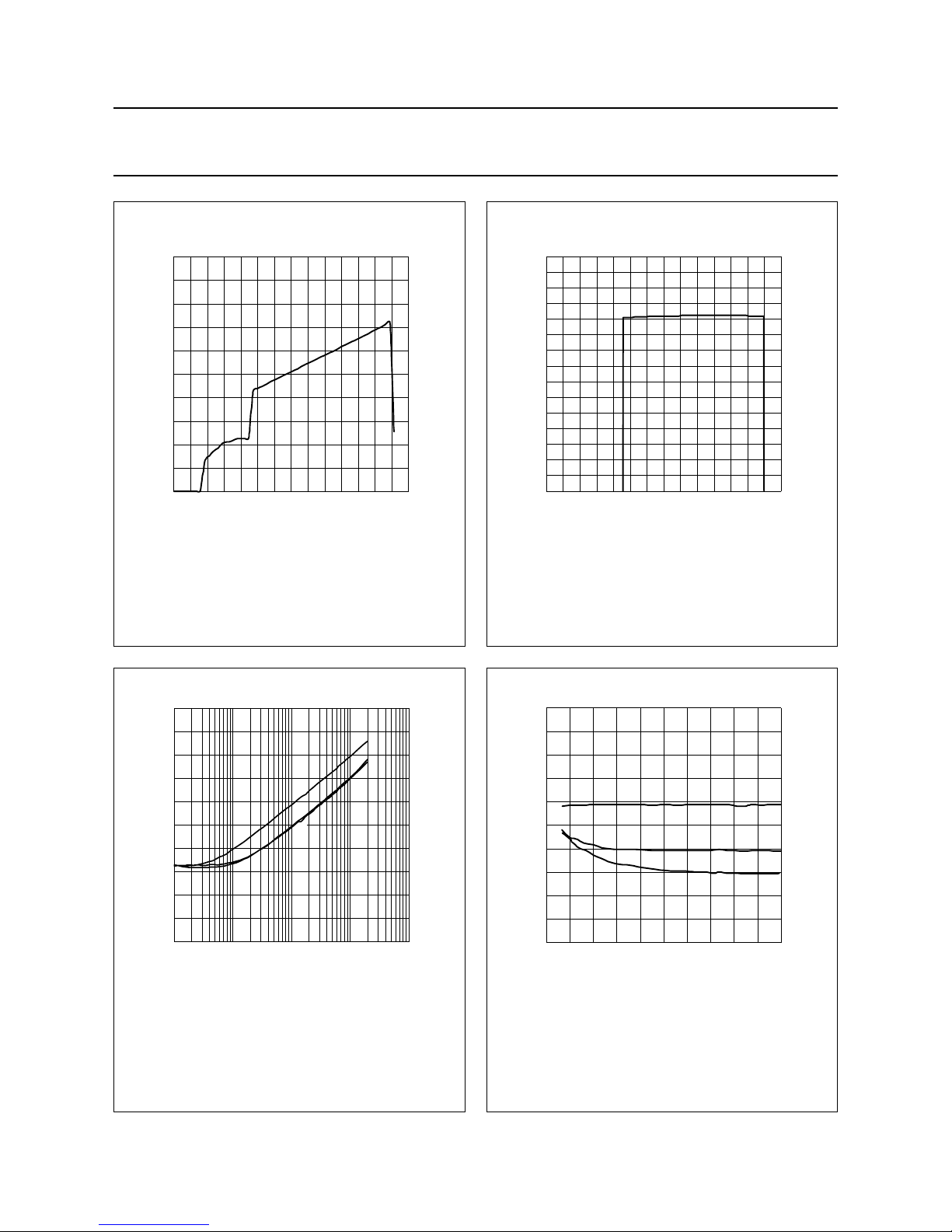
Fig.26 Quiescent current as a function of supply
voltage.
RL= ∞.
handbook, halfpage
f
clk
(kHz)
0 5 10 2515 30 35
VDD (V)
20
290
320
300
310
MGX339
Fig.27 Clock frequency as a function of supply
voltage.
RL= ∞.
handbook, halfpage
MGX346
SVRR
(dB)
−80
−100
−60
−20
−40
0
fi (Hz)
10 10
2
10
3
10
4
10
5
(2)
(1)
(3)
Fig.28 SVRR as a function of input frequency.
VP= ±20 V; V
ripple
= 2 V (p-p) with respect to ground.
(1) Both supply lines in phase.
(2) Both supply lines in anti-phase.
(3) One supply line rippled.
handbook, halfpage
SVRR)
(dB)
03145
V
ripple(p-p)
(V)
2
−100
0
−40
−20
−80
−60
MGX347
(1)
(2)
(3)
Fig.29 SVRR as a function of V
ripple(p-p)
.
VP= ±20 V; V
ripple
with respect to ground (in phase).
(1) f
ripple
= 1 kHz.
(2) f
ripple
= 100 Hz.
(3) f
ripple
=10Hz.
Page 27
2003 Mar 20 27
Philips Semiconductors Objective specification
2 × 25 W class-D power amplifier TDA8922
handbook, halfpage
MGX334
2
0
4
8
6
10
(1)
(2)
Po (W)
10
−2
10
−1
11010
2
V
ripple(p-p)
(V)
Fig.30 Supply voltage ripple as a function of output
power.
3000 µF per supply line; fi=10Hz.
(1) 1 × 4 Ω SE, VP= ±15 V.
(2) 1 × 8 Ω SE, VP= ±20 V.
handbook, halfpage
MGX335
V
ripple(p-p)
(V)
2
0
4
8
6
10
fi (Hz)
10 10
2
10
3
10
4
(1)
(2)
Fig.31 Supply voltage ripple as a function of input
frequency.
3000 µF per supply line.
(1) Po= 10 W into 1 × 4 Ω SE, VP= ±15 V.
(2) Po= 10 W into 1 × 8 Ω SE, VP= ±20 V.
handbook, halfpage
MGX342
100 400200 500 600
f
clk
(kHz)
300
THD + N
(%)
10
1
10
−1
10
−2
10
−3
(1)
(2)
(3)
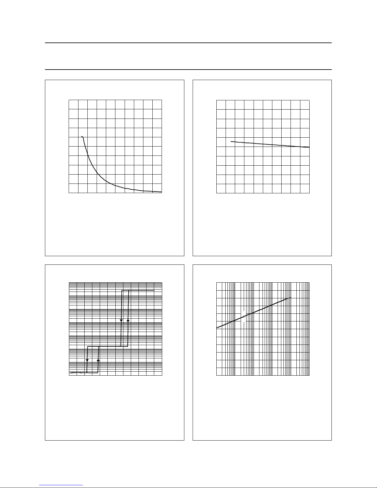
Fig.32 THD + N as a function of clock frequency.
VP= ±20 V; Po= 1 W into 8 Ω.
(1) 10 kHz.
(2) 1 kHz.
(3) 100 Hz.
handbook, halfpage
I
q
(mA)
100 400200 500 600
f
clk
(kHz)
300
0
150
90
120
30
60
MGX344
Fig.33 Quiescent current as a function of clock
frequency.
VP= ±20 V; RL= ∞.
Page 28
2003 Mar 20 28
Philips Semiconductors Objective specification
2 × 25 W class-D power amplifier TDA8922
handbook, halfpage
V
res(rms)
(mV)
100 400200 500 600
f
clk
(kHz)
300
0
1000
600
800
200
400
MGX345
Fig.34 PWM residual voltage as a function of clock
frequency.
VP= ±20 V; RL=8Ω.
handbook, halfpage
P
o
(W)
100 400200 500 600
f
clk
(kHz)
300
0
50
30
40
10
20
MGX343
Fig.35 Output power as a function of clock
frequency.
VP= ±20 V; RL=8Ω; fi= 1 kHz; THD+N=10%.
handbook, halfpage
MGX348
V
o
(V)
10
−4
10
−1
10
−5
10
−6
10
−3
10
−2
1
10
V
MODE
(V)
6543210
Fig.36 Output voltage as a function of mode
selection voltage.
Vi= 100 mV; fi= 1 kHz.
handbook, halfpage
MGX349
S/N
(dB)
40
80
20
0
60
100
120
Po (W)
10
−2
10
−1
110 10
3
10
2
(1)
(2)
Fig.36 Signal-to-noise ratio as a function of output
power.
VP= ±20 V; Rs= 5.6 kΩ.; filter: 20 kHz AES17
(1) 2 × 8 Ω SE.
(2) 1 × 8 Ω BTL.
Page 29
2003 Mar 20 29
Philips Semiconductors Objective specification
2 × 25 W class-D power amplifier TDA8922
This text is here in white to force landscape pages to be rotated correctly when browsing through the pdf in the Acrobat reader.This text is here in
_white to force landscape pages to be rotated correctly when browsing through the pdf in the Acrobat reader.This text is here inThis text is here in
white to force landscape pages to be rotated correctly when browsing through the pdf in the Acrobat reader. white to force landscape pages to be ...
16.13 Application schematics
handbook, full pagewidth
OUT1
V
SSP1
V
DDP2
DRIVER
HIGH
MGU998
OUT2
BOOT2
TDA8922TH
BOOT1
DRIVER
LOW
RELEASE1
SWITCH1
ENABLE1
CONTROL
AND
HANDSHAKE
PWM
MODULATOR
R
FB
R
FB
MANAGER
OSCILLATOR
TEMPERATURE SENSOR
CURRENT PROTECTION
STABI
MODE
R
OSC
V
SSA
V
mode
C
OSC
INPUT
STAGE
mute
9
8
IN1−
IN1+
22
21
2017
16
15
V
SSP2
V
SSP1
DRIVER
HIGH
DRIVER
LOW
RELEASE2
SWITCH2
ENABLE2
CONTROL
AND
HANDSHAKE
PWM
MODULATOR
11
SGND1
7
OSC
2
SGND2
SGND
SGND
6
MODE
INPUT
STAGE
mute
5
4
IN2−
IN2+
V
in2
V
in1
1924
V
SSD
V
SSA
V
SSP
0 V
V
SSA
−25 V
V
DDP
V
DDA
+25 V
HW
1
V
SSA2
V
SSA
12
V
SSA1
3
V
DDA2
V
DDA
10
V
DDA1
231318 14
V
DDP2
PROTSTABI
V
DDP1
SGND
Fig.37 Typical SE application schematic of TDA8922TH.
Page 30
2003 Mar 20 30
Philips Semiconductors Objective specification
2 × 25 W class-D power amplifier TDA8922
This text is here in white to force landscape pages to be rotated correctly when browsing through the pdf in the Acrobat reader.This text is here in
_white to force landscape pages to be rotated correctly when browsing through the pdf in the Acrobat reader.This text is here inThis text is here in
white to force landscape pages to be rotated correctly when browsing through the pdf in the Acrobat reader. white to force landscape pages to be ...
handbook, full pagewidth
OUT1
V
SSP1
V
DDP2
DRIVER
HIGH
MGU999
OUT2
BOOT2
TDA8922J
BOOT1
DRIVER
LOW
RELEASE1
SWITCH1
ENABLE1
CONTROL
AND
HANDSHAKE
PWM
MODULATOR
R
FB
R
FB
MANAGER
OSCILLATOR
TEMPERATURE SENSOR
CURRENT PROTECTION
STABI
MODE
R
OSC
V
SSA
V
mode
C
OSC
INPUT
STAGE
mute
3
2
IN1−
IN1+
15
14
1311
10
9
V
SSP2
V
SSP1
DRIVER
HIGH
DRIVER
LOW
RELEASE2
SWITCH2
ENABLE2
CONTROL
AND
HANDSHAKE
PWM
MODULATOR
5
SGND1
1
OSC
19
SGND2
SGND
SGND
23
MODE
INPUT
STAGE
mute
22
21
IN2−
IN2+
V
in2
V
in1
17
V
SSD
V
SSA
V
SSP
0 V
V
SSA
−25 V
V
DDP
V
DDA
+25 V
18
V
SSA2
V
SSA
6
V
SSA1
20
V
DDA2
V
DDA
4
V
DDA1
16712 8
V
DDP2
PROTSTABI
V
DDP1
SGND
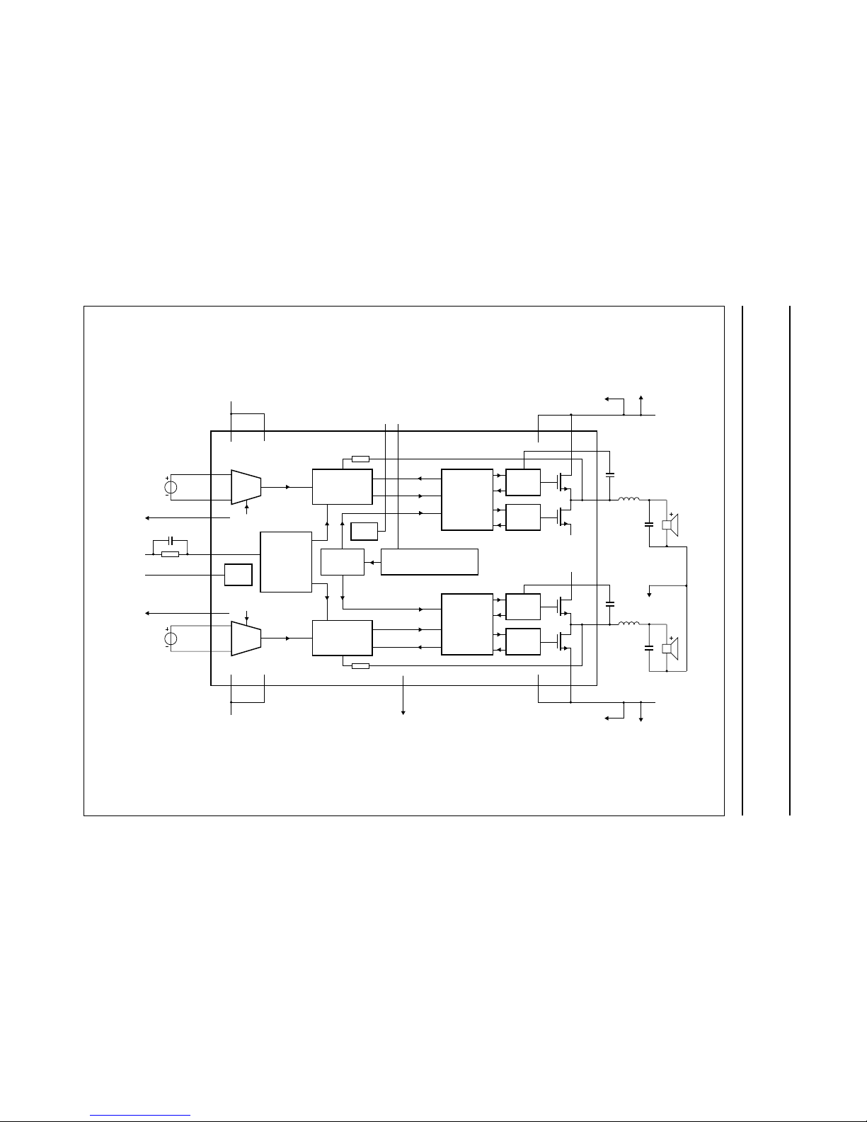
Fig.38 Typical SE application schematic of TDA8922J.
Page 31
2003 Mar 20 31
Philips Semiconductors Objective specification
2 × 25 W class-D power amplifier TDA8922
17 PACKAGE OUTLINES
UNIT
A
4
(1)
REFERENCES
OUTLINE
VERSION
EUROPEAN
PROJECTION
ISSUE DATE
02-01-30
03-02-18
IEC JEDEC JEITA
mm
+0.08
−0.04
3.5 0.35
DIMENSIONS (mm are the original dimensions)
Notes
1. Limits per individual lead.
2. Plastic or metal protrusions of 0.25 mm maximum per side are not included.
SOT566-3
0 5 10 mm
scale
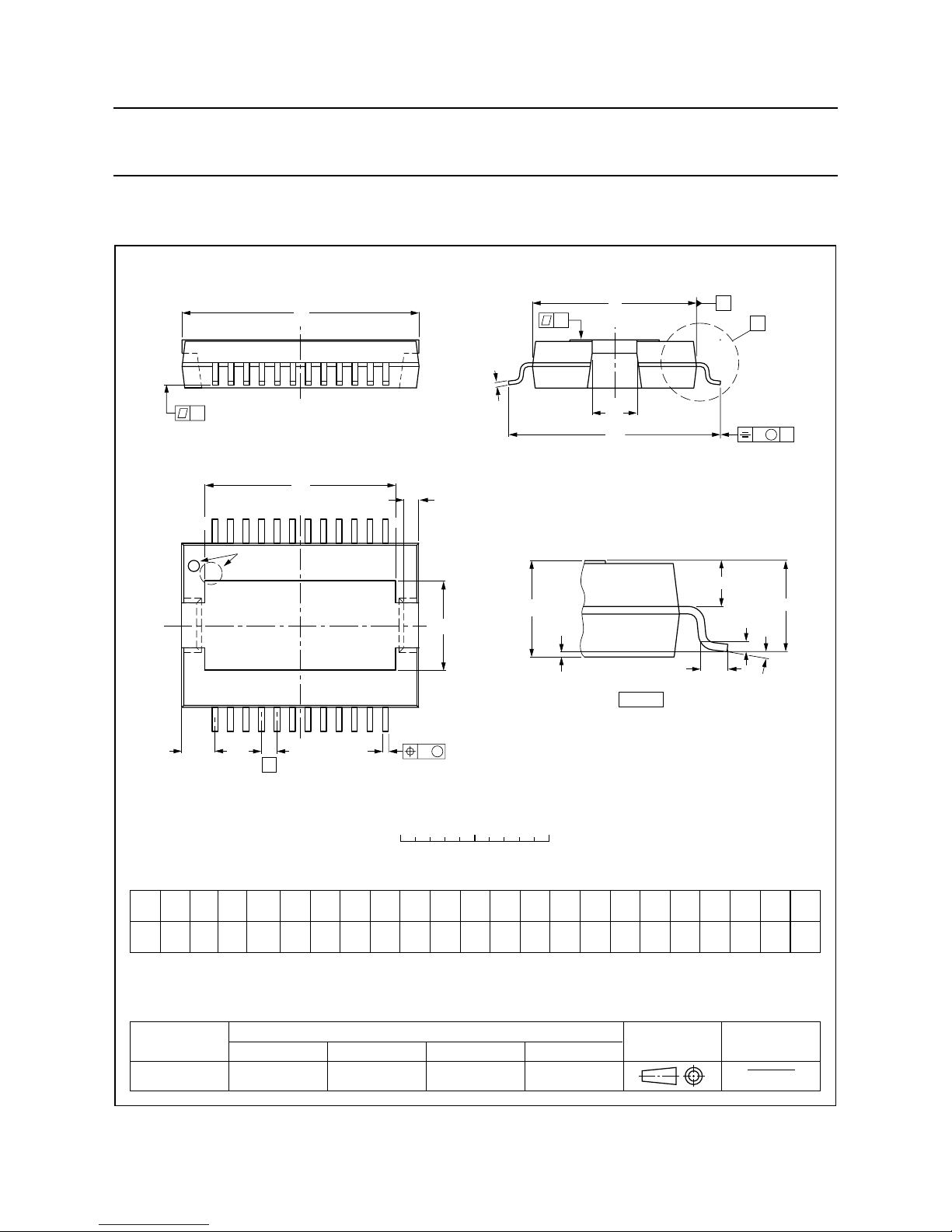
HSOP24: plastic, heatsink small outline package; 24 leads; low stand-off height
SOT566-3
A
max.
detail X
A
2
3.5
3.2
D
2
1.1
0.9
H
E
14.5
13.9
L
p
1.1
0.8
Q
1.7
1.5
2.7
2.2
v
0.25w0.25
yZ
8°
0°
θ
0.07
x
0.03
D
1
13.0
12.6
E
1
6.2
5.8
E
2
2.9
2.5
bpc
0.32
0.23
e
1
D
(2)
16.0
15.8
E
(2)
11.1
10.9
0.53
0.40
A
3
A
4
A
2
(A3)
L
p
θ
A
Q
D
y
x
H
E
E
c
v M
A
X
A
b
p
w M
Z
D
1
D
2
E
2
E
1
e
24
13
1
12
pin 1 index
Page 32
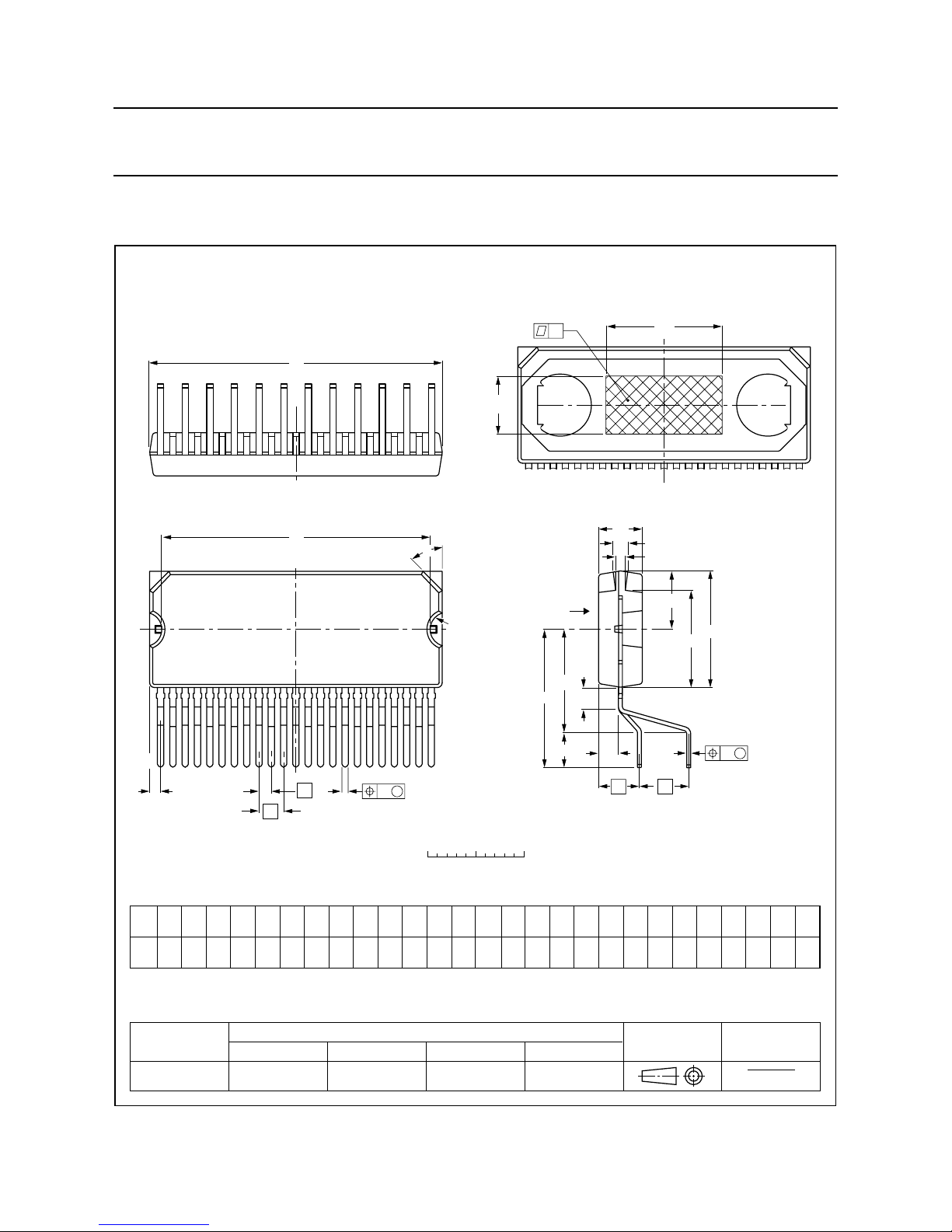
2003 Mar 20 32
Philips Semiconductors Objective specification
2 × 25 W class-D power amplifier TDA8922
UNIT A
2
REFERENCES
OUTLINE
VERSION
EUROPEAN
PROJECTION
ISSUE DATE
IEC JEDEC JEITA
mm
4.6
4.3
A
4
1.15
0.85
A
5
1.65
1.35
DIMENSIONS (mm are the original dimensions)
Note
1. Plastic or metal protrusions of 0.25 mm maximum per side are not included.
SOT411-1
98-02-20
02-04-24
0 5 10 mm
scale
D
L
L
1
L
2
E
2
E
c
A
4
A
5
A
2
m
L
3
E
1
Q
w M
b
p
1
d
Z
e
2
e
e
123
j
DBS23P: plastic DIL-bent-SIL power package; 23 leads (straight lead length 3.2 mm)
SOT411-1
v M
D
x
h
E
h
non-concave
view B: mounting base side
B
β
e
1
bpcD
(1)
E
(1)
Z
(1)
deD
h
LL
3
m
0.75
0.60
0.55
0.35
30.4
29.9
28.0
27.5
12 2.54
12.2
11.8
10.15
9.85
1.27
e
2
5.08
2.4
1.6
E
h
6
E
1
14
13
L
1
10.7
9.9
L
2
6.2
5.8
E
2
1.43
0.78
2.1
1.8
1.85
1.65
4.3
3.6
2.8
Qj
0.25
w
0.6
v
0.03x45°
β
Page 33

2003 Mar 20 33
Philips Semiconductors Objective specification
2 × 25 W class-D power amplifier TDA8922
18 SOLDERING
18.1 Introduction
Thistextgivesaverybriefinsight to a complex technology.
A more in-depth account of soldering ICs can be found in
our
“Data Handbook IC26; Integrated Circuit Packages”
(document order number 9398 652 90011).
There is no soldering method that is ideal for all IC
packages. Wave soldering is often preferred when
through-holeandsurface mount components are mixed on
one printed-circuit board. Wave soldering can still be used
for certain surface mount ICs, but it is not suitable for fine
pitch SMDs. In these situations reflow soldering is
recommended.
18.2 Through-hole mount packages
18.2.1 SOLDERING BY DIPPING OR BY SOLDER WAVE
The maximum permissible temperature of the solder is
260 °C; solder at this temperature must not be in contact
with the joints for more than 5 seconds. The total contact
time of successive solder waves must not exceed
5 seconds.
The device may be mounted up to the seating plane, but
the temperature of the plastic body must not exceed the
specified maximum storage temperature (T
stg(max)
). If the
printed-circuit board has been pre-heated, forced cooling
may be necessary immediately after soldering to keep the
temperature within the permissible limit.
18.2.2 MANUAL SOLDERING
Apply the soldering iron (24 V or less) to the lead(s) of the
package, either below the seating plane or not more than
2 mm above it. If the temperature of the soldering iron bit
is less than 300 °C it may remain in contact for up to
10 seconds. If the bit temperature is between
300 and 400 °C, contact may be up to 5 seconds.
18.3 Surface mount packages
18.3.1 REFLOW SOLDERING
Typical reflow peak temperatures range from
215 to 250 °C. The top-surface temperature of the
packages should preferably be kept:
• below 220 °C for all the BGA packages and packages
with a thickness 2.5mm and packages with a thickness
<2.5 mm and a volume ≥350 mm3 so called thick/large
packages
• below 235 °C for packages with a thickness <2.5 mm
and a volume <350 mm3 so called small/thin packages.
18.3.2 WAVE SOLDERING
Conventional single wave soldering is not recommended
forsurfacemountdevices(SMDs)orprinted-circuitboards
with a high component density, as solder bridging and
non-wetting can present major problems.
To overcome these problems the double-wave soldering
method was specifically developed.
If wave soldering is used the following conditions must be
observed for optimal results:
• Use a double-wave soldering method comprising a
turbulent wave with high upward pressure followed by a
smooth laminar wave.
• For packages with leads on two sides and a pitch (e):
– larger than or equal to 1.27 mm, the footprint
longitudinal axis is preferred to be parallel to the
transport direction of the printed-circuit board;
– smaller than 1.27 mm, the footprint longitudinal axis
must be parallel to the transport direction of the
printed-circuit board.
The footprint must incorporate solder thieves at the
downstream end.
• Forpackageswithleadsonfoursides,thefootprintmust
be placed at a 45° angle to the transport direction of the
printed-circuit board. The footprint must incorporate
solder thieves downstream and at the side corners.
During placement and before soldering, the package must
be fixed with a droplet of adhesive. The adhesive can be
applied by screen printing, pin transfer or syringe
dispensing. The package can be soldered after the
adhesive is cured.
Typical dwell time is 4 seconds at 250 °C.
A mildly-activated flux will eliminate the need for removal
of corrosive residues in most applications.
18.3.3 MANUAL SOLDERING
Fix the component by first soldering two
diagonally-opposite end leads. Use a low voltage (24 V or
less) soldering iron applied to the flat part of the lead.
Contact time must be limited to 10 seconds at up to
300 °C. When using a dedicated tool, all other leads can
be soldered in one operation within 2 to 5 seconds
between 270 and 320 °C.
Page 34

2003 Mar 20 34
Philips Semiconductors Objective specification
2 × 25 W class-D power amplifier TDA8922
18.4 Suitability of IC packages for wave, reflow and dipping soldering methods
Notes
1. Formoredetailed information on the BGA packages refer tothe
“(LF)BGAApplication Note
”(AN01026);order a copy
from your Philips Semiconductors sales office.
2. All surface mount (SMD) packages are moisture sensitive. Depending upon the moisture content, the maximum
temperature (with respect to time) and body size of the package, there is a risk that internal or external package
cracks may occur due to vaporization of the moisture in them (the so called popcorn effect). For details, refer to the
Drypack information in the
“Data Handbook IC26; Integrated Circuit Packages; Section: Packing Methods”
.
3. For SDIP packages, the longitudinal axis must be parallel to the transport direction of the printed-circuit board.
4. These packages are not suitable for wave soldering. On versions with the heatsink on the bottom side, the solder
cannot penetrate between the printed-circuit board and the heatsink. On versions with the heatsink on the top side,
the solder might be deposited on the heatsink surface.
5. If wave soldering is considered, then the package must be placed at a 45° angle to the solder wave direction.
The package footprint must incorporate solder thieves downstream and at the side corners.
6. Wave soldering is suitable for LQFP, QFP and TQFP packages with a pitch (e) larger than 0.8 mm; it is definitely not
suitable for packages with a pitch (e) equal to or smaller than 0.65 mm.
7. Wave soldering is suitable for SSOP, TSSOP, VSO and VSSOP packages with a pitch (e) equal to or larger than
0.65 mm; it is definitely not suitable for packages with a pitch (e) equal to or smaller than 0.5 mm.
MOUNTING PACKAGE
(1)
SOLDERING METHOD
WAVE REFLOW
(2)
DIPPING
Through-hole mount DBS, DIP, HDIP, SDIP, SIL suitable
(3)
− suitable
Surface mount BGA, LBGA, LFBGA, SQFP, TFBGA, VFBGA not suitable suitable −
DHVQFN, HBCC, HBGA, HLQFP, HSQFP,
HSOP, HTQFP, HTSSOP, HVQFN, HVSON,
SMS
not suitable
(4)
suitable −
PLCC
(5)
, SO, SOJ suitable suitable −
LQFP, QFP, TQFP not recommended
(5)(6)
suitable −
SSOP, TSSOP, VSO, VSSOP not recommended
(7)
suitable −
Page 35

2003 Mar 20 35
Philips Semiconductors Objective specification
2 × 25 W class-D power amplifier TDA8922
19 DATA SHEET STATUS
Notes
1. Please consult the most recently issued data sheet before initiating or completing a design.
2. The product status of the device(s) described in this data sheet may have changed since this data sheet was
published. The latest information is available on the Internet at URL http://www.semiconductors.philips.com.
3. For data sheets describing multiple type numbers, the highest-level product status determines the data sheet status.
LEVEL
DATA SHEET
STATUS
(1)
PRODUCT
STATUS
(2)(3)
DEFINITION
I Objective data Development This data sheet contains data from the objective specification for product
development. Philips Semiconductors reserves the right to change the
specification in any manner without notice.
II Preliminary data Qualification This data sheet contains data from the preliminary specification.
Supplementary data will be published at a later date. Philips
Semiconductors reserves the right to change the specification without
notice, in order to improve the design and supply the best possible
product.
III Product data Production This data sheet contains data from the product specification. Philips
Semiconductors reserves the right to make changes at any time in order
to improve the design, manufacturing and supply. Relevant changes will
be communicated via a Customer Product/Process Change Notification
(CPCN).
20 DEFINITIONS
Short-form specification The data in a short-form
specification is extracted from a full data sheet with the
same type number and title. For detailed information see
the relevant data sheet or data handbook.
Limiting values definition Limiting values given are in
accordance with the Absolute Maximum Rating System
(IEC 60134). Stress above one or more of the limiting
values may cause permanent damage to the device.
These are stress ratings only and operation of the device
attheseorat any other conditions above those given in the
Characteristics sections of the specification is not implied.
Exposure to limiting values for extended periods may
affect device reliability.
Application information Applications that are
described herein for any of these products are for
illustrative purposes only. Philips Semiconductors make
norepresentationorwarrantythatsuch applications will be
suitable for the specified use without further testing or
modification.
21 DISCLAIMERS
Life support applications These products are not
designed for use in life support appliances, devices, or
systems where malfunction of these products can
reasonably be expected to result in personal injury. Philips
Semiconductorscustomersusingorselling these products
for use in such applications do so at their own risk and
agree to fully indemnify Philips Semiconductors for any
damages resulting from such application.
Right to make changes Philips Semiconductors
reserves the right to make changes in the products including circuits, standard cells, and/or software described or contained herein in order to improve design
and/or performance. When the product is in full production
(status ‘Production’), relevant changes will be
communicated via a Customer Product/Process Change
Notification (CPCN). Philips Semiconductors assumes no
responsibility or liability for the use of any of these
products, conveys no licence or title under any patent,
copyright, or mask work right to these products, and
makes no representations or warranties that these
products are free from patent, copyright, or mask work
right infringement, unless otherwise specified.
Page 36

© Koninklijke Philips Electronics N.V. 2003
SCA75
All rights are reserved. Reproduction in whole or in part is prohibited without the prior written consent of the copyright owner.
The information presented in this document does not form part of any quotation or contract, is believed to be accurate and reliable and may be changed
without notice. No liability will be accepted by the publisher for any consequence of its use. Publication thereof does not convey nor imply any license
under patent- or other industrial or intellectual property rights.
Philips Semiconductors – a w orldwide compan y
Contact information
For additional information please visit http://www.semiconductors.philips.com. Fax: +31 40 27 24825
For sales offices addresses send e-mail to: [email protected].
Printed in The Netherlands 753503/01/pp36 Date of release: 2003 Mar 20 Document order number: 9397 750 10757
 Loading...