

Page 1

DATA SH EET
Preliminary specification
File under Integrated Circuits, IC01
2002 Jan 14
INTEGRATED CIRCUITS
TDA8591J
4 × 44 W into 4 Ω or 4 × 75 W
into 2 Ω quad BTL car radio power
amplifier
Page 2

2002 Jan 14 2
Philips Semiconductors Preliminary specification
4 × 44 W into 4 Ω or 4 × 75 W into 2 Ω
quad BTL car radio power amplifier
TDA8591J
CONTENTS
1 FEATURES
2 GENERAL DESCRIPTION
3 ORDERING INFORMATION
4 QUICK REFERENCE DATA
5 BLOCK DIAGRAM
6 PINNING
7 FUNCTIONAL DESCRIPTION
7.1 Diagnostic facility
7.2 Diagnostic output (DIAG)
7.3 Mute timer and single-pin mute control
7.4 Output power
8 LIMITING VALUES
9 THERMAL CHARACTERISTICS
10 QUALITY SPECIFICATION
11 DC CHARACTERISTICS
12 AC CHARACTERISTICS
12.1 Performance curves
13 TEST INFORMATION
13.1 Protection circuit testing
14 APPLICATION INFORMATION
14.1 Special attention for SMD input capacitors
14.2 Capacitors on outputs
14.3 EMC precautions
14.4 Offset detection
14.5 Channel selection
14.6 Detection of short-circuits
14.7 PCB layout
14.8 PCB design advice
15 PACKAGE OUTLINE
16 SOLDERING
16.1 Introduction to soldering through-hole mount
packages
16.2 Soldering by dipping or by solder wave
16.3 Manual soldering
16.4 Suitability of through-hole mount IC packages
for dipping and wave soldering methods
17 DATA SHEET STATUS
18 DEFINITIONS
19 DISCLAIMERS
Page 3

2002 Jan 14 3
Philips Semiconductors Preliminary specification
4 × 44 W into 4 Ω or 4 × 75 W into 2 Ω
quad BTL car radio power amplifier
TDA8591J
1 FEATURES
• Low quiescent current
• Low distortion
• Low output offset voltage
• Soft thermal clipping to prevent audio holes
• External mute timer for low start-up plop (also allows a
fast mute function)
• High output power
• Operating, muteand standby mode selection by two-pin
or single-pin operation
• Diagnostic information available:
– Dynamic Distortion Detection (DDD)
– High temperature detection
– Short-circuit detection
– Detection of output offset due to leakage current at
the input
• No switch-on/switch-off plops when switching between
standby and mute modes or between mute and
operating modes
• Fast mute with supply voltage drops
• Package with flexible leads
• All outputscan withstand short-circuits to ground, to the
positive supply voltage and across the load
• Pin CP can withstand short-circuits to its adjacent pins,
all other pins can withstand short-circuits to ground and
to the positive supply voltage
• ESD protection on all pins
• Thermal protection against junction temperatures
exceeding 150 °C
• Load dump protection
• Protectedagainst opengroundpins (lossofground) and
outputs short-circuited to supply ground
• All negative outputs are protected against open supply
voltage and output short-circuited to supply voltage
• Reverse-polarity safe.
2 GENERAL DESCRIPTION
The TDA8591J is a quad BTL audio power amplifier
comprising four independent amplifiers in Bridge Tied
Load (BTL) configuration. Each amplifier has a gain of
26 dB and supplies an output power of 75 W (EIAJ) into a
2 Ω load.The TDA8591J has low quiescent current and is
primarily developed for car audio applications.
3 ORDERING INFORMATION
TYPE
NUMBER
PACKAGE
NAME DESCRIPTION VERSION
TDA8591J DBS27P plastic DIL-bent-SIL power package; 27 leads (lead length 7.7 mm) SOT521-1
Page 4

2002 Jan 14 4
Philips Semiconductors Preliminary specification
4 × 44 W into 4 Ω or 4 × 75 W into 2 Ω
quad BTL car radio power amplifier
TDA8591J
4 QUICK REFERENCE DATA
SYMBOL PARAMETER CONDITIONS MIN. TYP. MAX. UNIT
V
P
supply voltage 8.0 14.4 18.0 V
I
q(tot)
total quiescent current 120 200 290 mA
I
stb
standby supply current − 250µA
Z
i
input impedance − 70 − kΩ
P
o
output power THD+N=0.5%
R
L
=4Ω 19 22 − W
R
L
=2Ω−34 − W
THD+N=10%
RL=4Ω 27 28 − W
R
L
=2Ω−47 − W
EAIJ values
R
L
=4Ω 41.5 44 − W
R
L
=2Ω−75 − W
V
OO
output offset voltage mute mode −−30 mV
DC operating mode −−60 mV
G
v
voltage gain Vi= 40 mV (RMS) 25 26 27 dB
THD + N total harmonic distortion
plus noise
P
o
= 1 W; f = 1 kHz; RL=4Ω− 0.03 0.1 %
α
cs
channel separation Vi= 40 mV (RMS); Rs=0Ω 56 68 − dB
V
n(o)
noise output voltage Rs=0Ω; see Fig.29 − 70 −µV
SVRR supply voltage ripple
rejection
V
ripple
= 2 V (p-p); mute or
operating mode; Rs=0Ω;
see Fig.29
54 68 − dB
Page 5
2002 Jan 14 5
Philips Semiconductors Preliminary specification
4 × 44 W into 4 Ω or 4 × 75 W into 2 Ω
quad BTL car radio power amplifier
TDA8591J
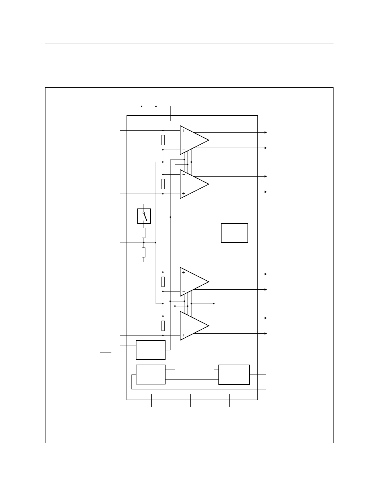
5 BLOCK DIAGRAM
MGW449
handbook, full pagewidth
26 dB
26 dB
26 dB
10
12
22
2
16
18
20
4
PGND1
8
3
5
26 dB
V
P
INTERFACE
STBY
MUTE/ON
OFFSET
DETECTION
7
PGND221PGND324PGND427GNDHS
DIAGNOSTIC
CHARGE
PUMP
TDA8591J
1
V
P1
V
P
13
V
P2
15
V
P3
OUT1−
OUT1+
9
11
OUT2+
OUT2−
14
CP
6
DIAG
26
OFFCAP
19
17
OUT3+
OUT3−
25
23
OUT4−
OUT4+
IN4
IN3
SGND
CIN
IN2
IN1
Fig.1 Block diagram.
Page 6
2002 Jan 14 6
Philips Semiconductors Preliminary specification
4 × 44 W into 4 Ω or 4 × 75 W into 2 Ω
quad BTL car radio power amplifier
TDA8591J
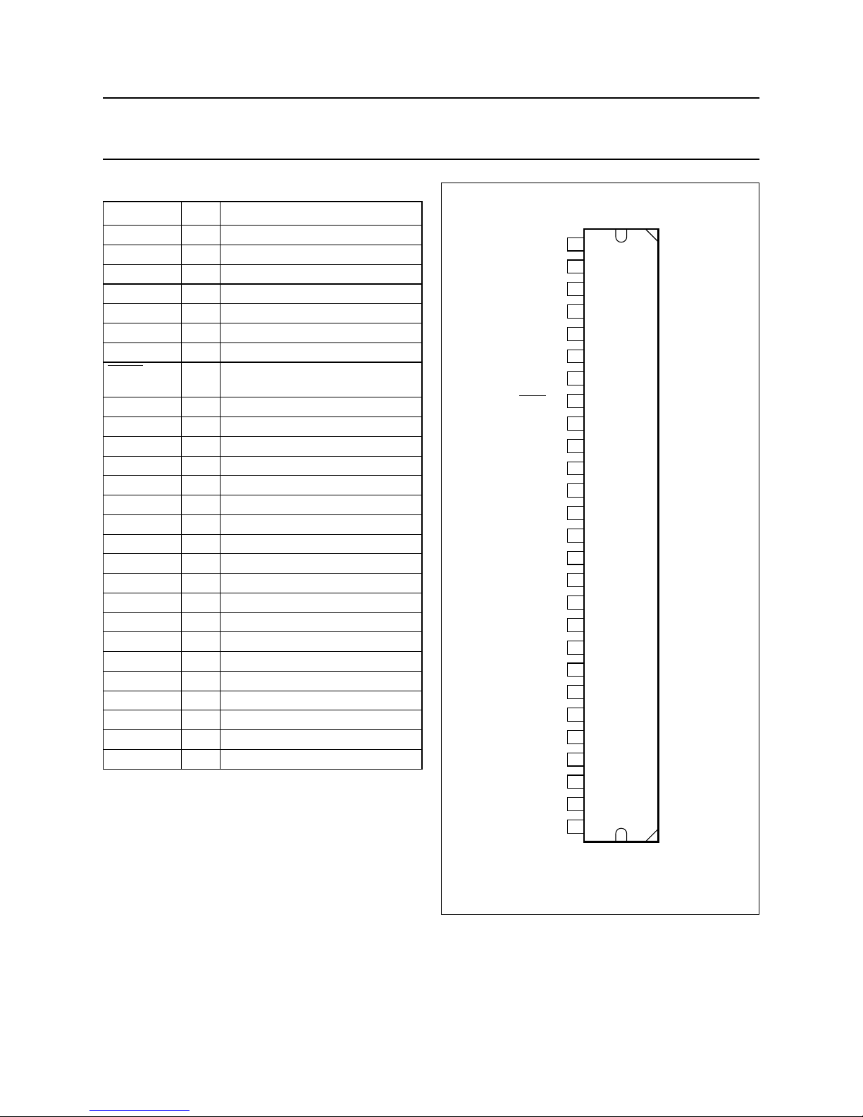
6 PINNING
SYMBOL PIN DESCRIPTION
V
P1
1 power supply to channels 1 and 4
SGND 2 signal ground
OUT1− 3 channel 1 negative output
PGND1 4 channel 1 power ground
OUT1+ 5 channel 1 positive output
DIAG 6 diagnostic output
PGND2 7 channel 2 power ground
MUTE/ON 8 mode select input: mute/amplifier
operating (via mute timer)
OUT2+ 9 channel 2 positive output
IN1 10 channel 1 input
OUT2− 11 channel 2 negative output
IN2 12 channel 2 input
V
P2
13 channel 2 power supply
CP 14 charge pump capacitor
V
P3
15 channel 3 power supply
IN3 16 channel 3 input
OUT3− 17 channel 3 negative output
IN4 18 channel 4 input
OUT3+ 19 channel 3 positive output
STBY 20 standby select input
PGND3 21 channel 3 power ground
CIN 22 common input voltage
OUT4+ 23 channel 4 positive output
PGND4 24 channel 4 power ground
OUT4− 25 channel 4 negative output
OFFCAP 26 offset detection capacitor
GNDHS 27 ground (heatsink of encapsulation)
handbook, halfpage
TDA8591J
MGW450
1
2
3
4
5
6
7
8
9
10
11
12
13
14
15
16
17
18
19
20
21
22
23
24
25
26
27
V
P1
SGND
OUT1−
PGND1
OUT1+
DIAG
PGND2
MUTE/ON
OUT2+
IN1
OUT2−
IN2
V
P2
CP
V
P3
IN3
OUT3−
IN4
OUT3+
STBY
PGND3
CIN
OUT4+
PGND4
OUT4−
OFFCAP
GNDHS
Fig.2 Pin configuration.
Page 7

2002 Jan 14 7
Philips Semiconductors Preliminary specification
4 × 44 W into 4 Ω or 4 × 75 W into 2 Ω
quad BTL car radio power amplifier
TDA8591J
7 FUNCTIONAL DESCRIPTION
The TDA8591J is an audio power amplifier with four
independent Bridge Tied Load (BTL) amplifiers with high
outputpower andlow distortion.The gainof eachamplifier
is fixed at 26 dB. The TDA8591J has two-pin mode control
which allows theamplifiers to be switched to standby (off)
with the STBY pin, and the MUTE/ON pin to be used to
switch betweenmute mode (input signalsuppressed) and
amplifier operating mode.
Special attention is paid to dynamic behaviour:
• A fast mute that switches all amplifiers to mute mode at
low supplyvoltage and suppresses noise during engine
start
• No plops when switching between standby and mute
modes
• Slow offset change when switching from mute mode to
operating mode (can be adjusted by an external
capacitor)
• A fast mute function by discharging the external mute
capacitor quickly
The following protection circuits are included to prevent
the IC from being damaged:
• Thermal shutdown:
At junction temperature Tvj> 170 °C, all power stages
are switched off to prevent a further increase in
temperature
• Soft thermal clipping:
At junction temperature Tvj> 155 °C, the gain reduces
astemperature increases,resulting inless outputpower
and decreasing temperature and therefore no thermal
shutdown (no break in the audio)
• Short-circuit protection:
If a short-circuit to ground or supply voltage occurs at
one or more ofthe output pins, or acrossthe load of one
or more of the channels, the following action occurs to
reduce power dissipation and case temperature
(see Figs 5 and 6):
– All amplifiers switch off for approximately 20 ms
– After 20 ms the amplifiers switch on again
– Ifthe short-circuit persists,theamplifiers switchofffor
another 20 ms period and the action repeats
• ESD protection:
– Human body model 2000V
– Machine model 200 V
• Protection against open ground pins and outputs
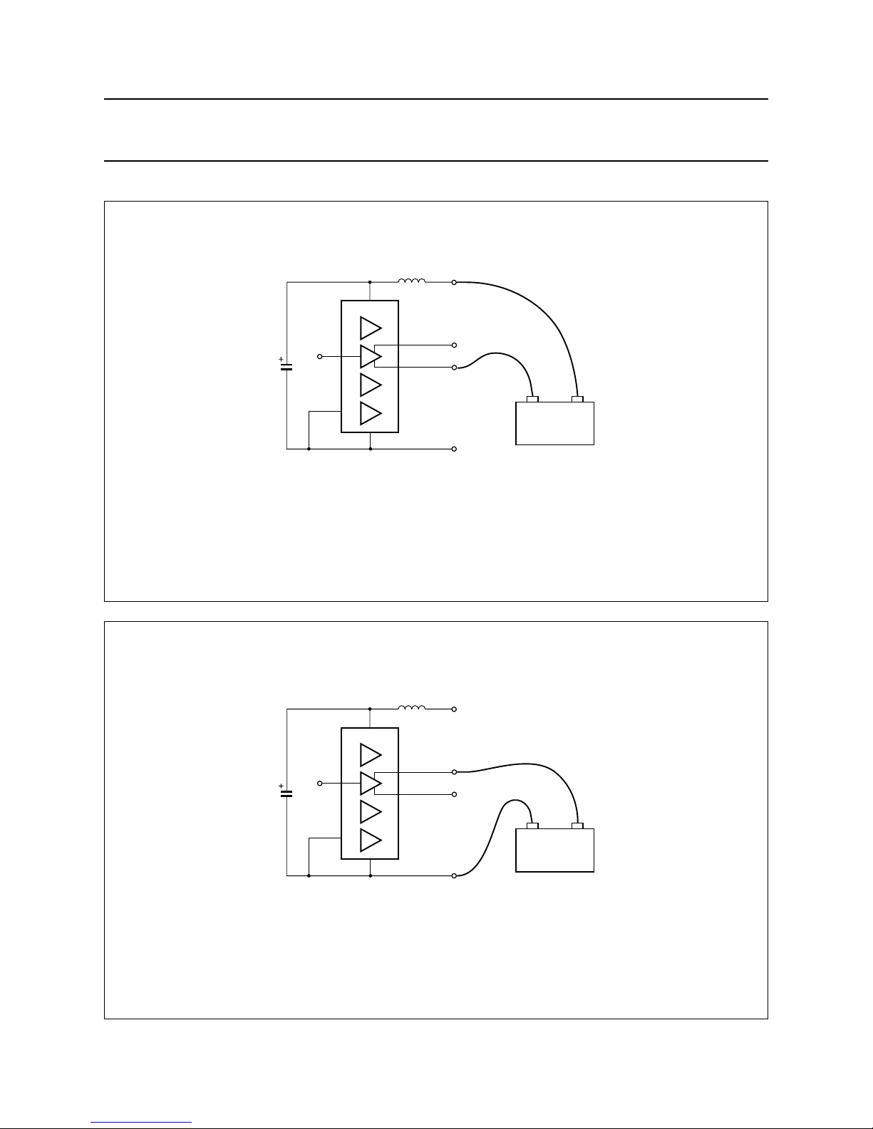
short-circuited to supply ground (see Fig.30)
• All outputs protected are against open power supply
pins and outputs short-circuitedto powersupply voltage
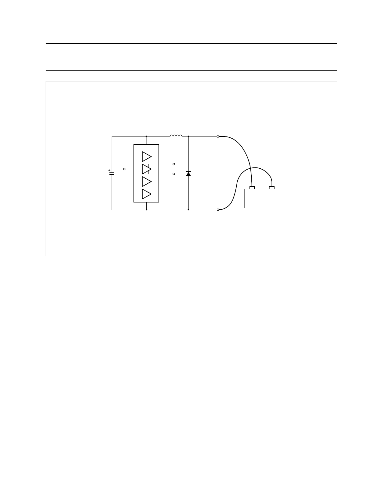
(see Fig.31)
• With areversed polarity powersupply an external diode
conducts and a fuse blows and therefore the reversed
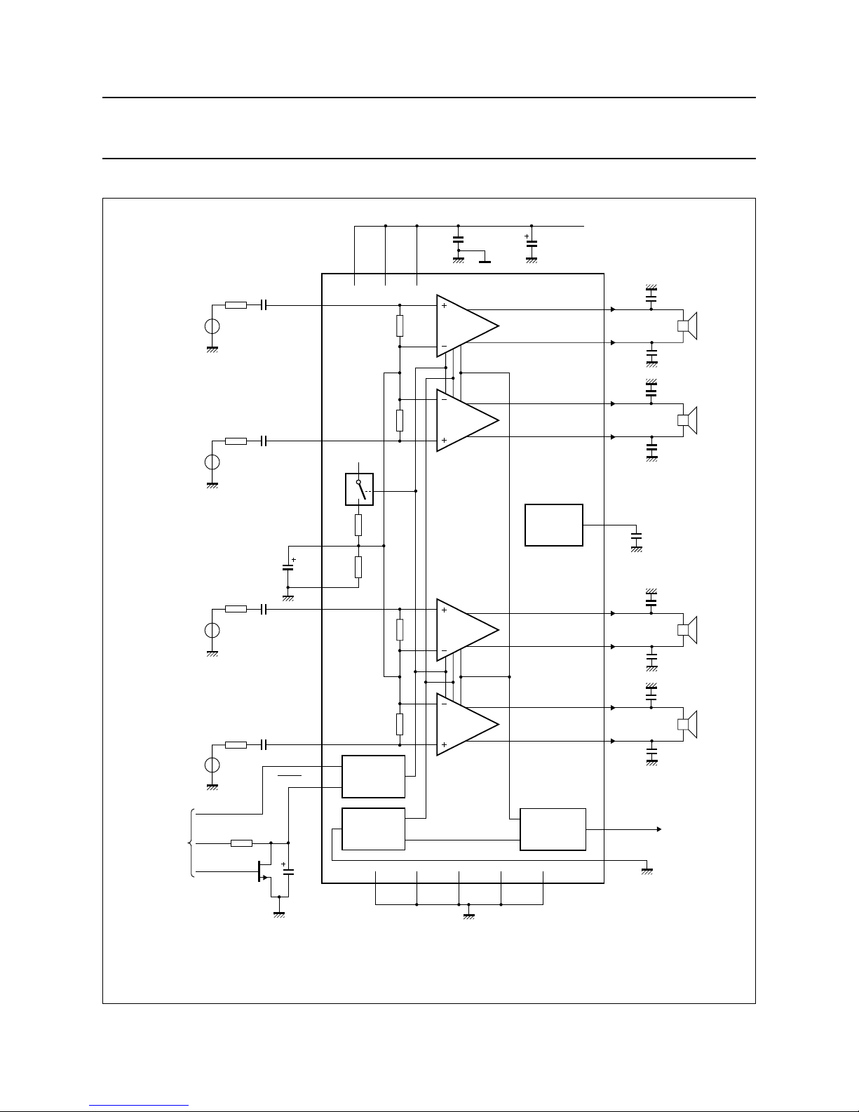
polarity voltage will not damage the device (see Fig.32).
7.1 Diagnostic facility
Adiagnostic facilityisavailable fromthestatus ofpin DIAG
for the following conditions:
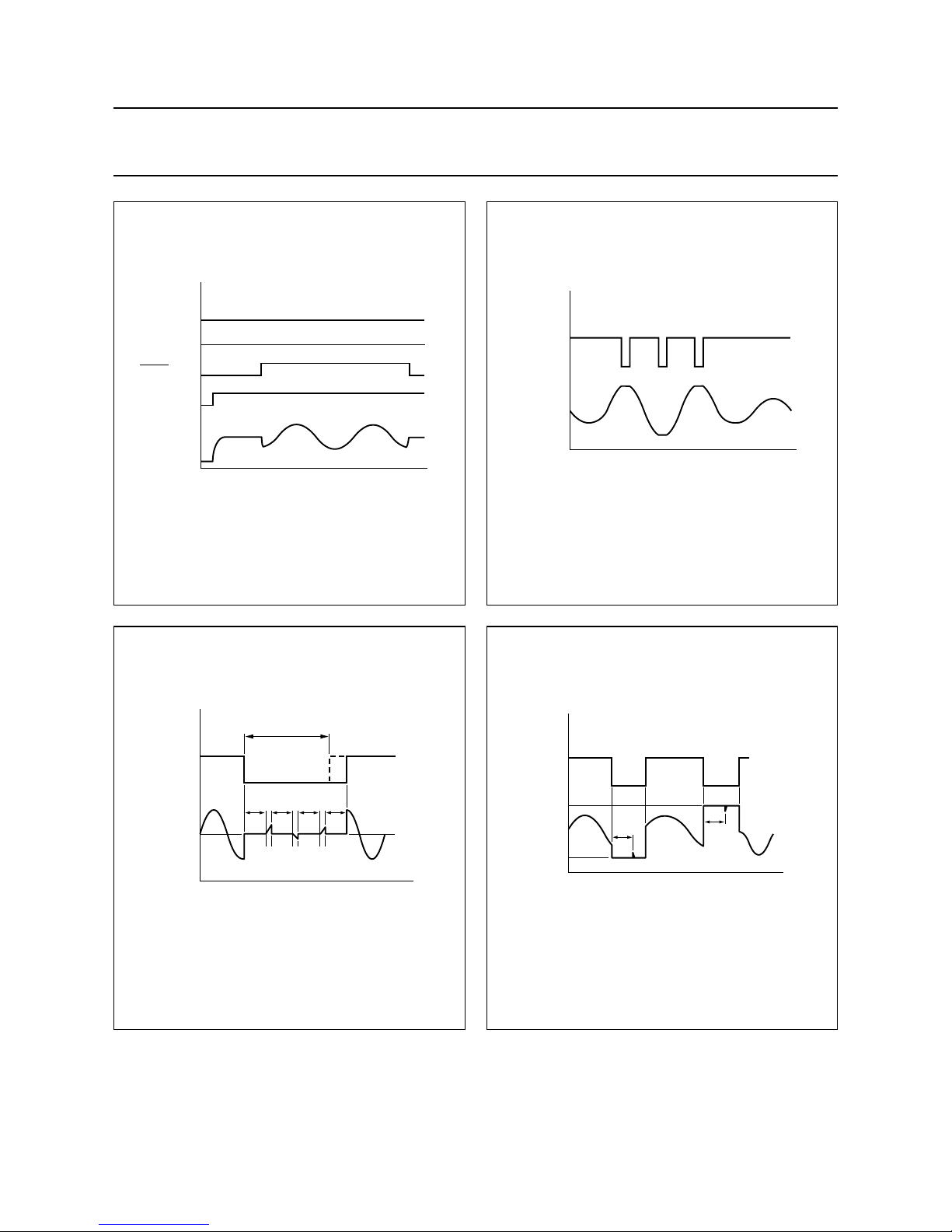
• In normal operation, the level on the DIAG pin is
continuously HIGH (see Fig.3)
• When a temperature pre-warning occurs due to the
junction temperature Tvjreaching 145 °C, the DIAG pin
goes continuously LOW
• When there is distortion over 2.5% because of clipping,
the DIAG pin has a pulsed output as shown in Fig.4
• When a short-circuit is detected, the short-circuit
protection becomesactive andDIAG goes continuously
LOW for the period of the short-circuit (see Figs 5 and 6)
• With an extreme output offset, input leakage current
causes a DC output offset voltage and results in power
dissipation in the loudspeakers. Therefore, if the
DC output offset voltage of a bridge is larger than 2 V,
DIAG is pulled LOW to indicate an error condition.
The DIAG pin has an open-drain output to allow several
devices to be tied together. An external pull-up resistor is
needed.
Page 8
2002 Jan 14 8
Philips Semiconductors Preliminary specification
4 × 44 W into 4 Ω or 4 × 75 W into 2 Ω
quad BTL car radio power amplifier
TDA8591J
andbook, halfpage
MGU489
amplifier
output
STBY
MUTE/ON
DIAG
play normal
mute
t (ms)
standby
operating
Fig.3 Diagnostic waveforms: standby, mute and
operating mode sequence.
Pull-up resistor = 47 kΩ.
handbook, halfpage
MGT605
normal
active
DDD
normal
amplifier
output
DIAG
t (ms)
Pull-up resistor = 47 kΩ.
Fig.4 Diagnostic waveforms: dynamic distortion
detection function.
andbook, halfpage
MGT604
amplifier
output
DIAG
short-circuit
across load
20 ms
t (ms)
Fig.5 Diagnostic waveforms: short-circuit across
load.
Pull-up resistor = 47 kΩ.
ndbook, halfpage
MGU498
short to
GND
short to
V
P
amplifier
output
DIAG
GND
20 ms
20 ms
V
P
t (ms)
Fig.6 Diagnostic waveforms: short-circuit to
VPpin or GND.
Pull-up resistor = 47 kΩ.
Page 9
2002 Jan 14 9
Philips Semiconductors Preliminary specification
4 × 44 W into 4 Ω or 4 × 75 W into 2 Ω
quad BTL car radio power amplifier
TDA8591J
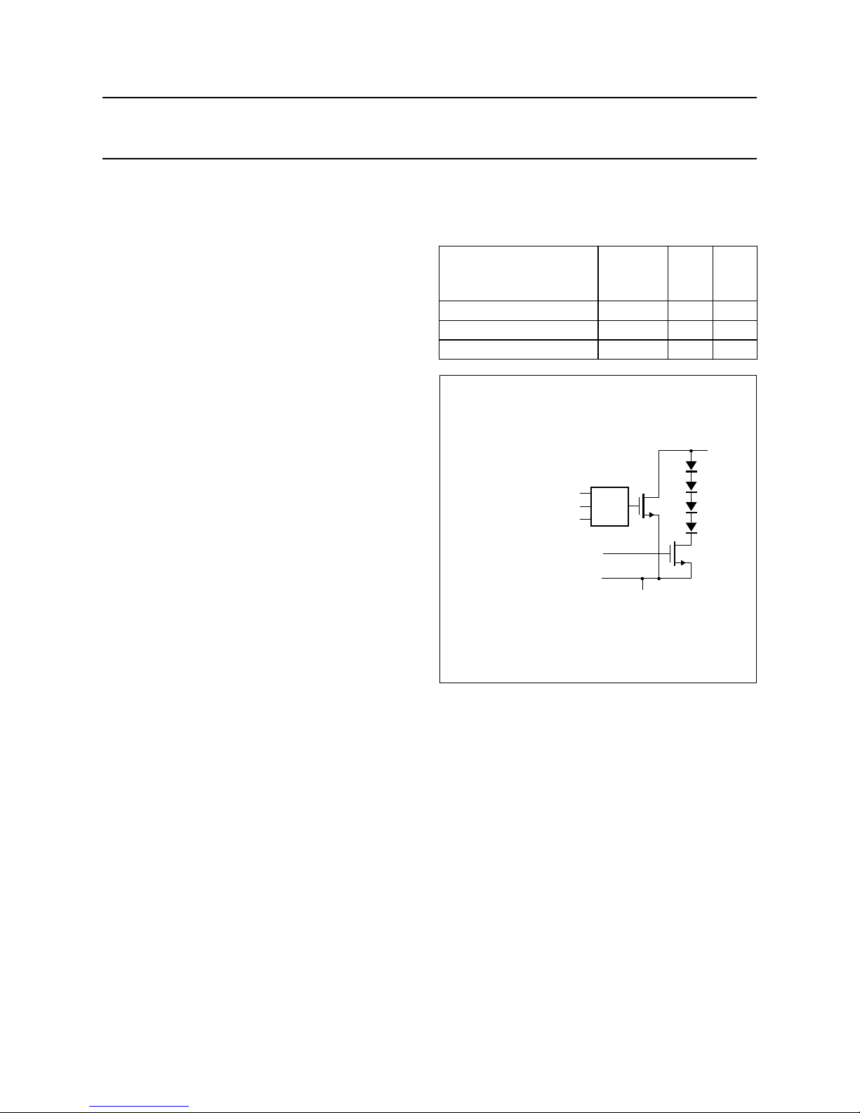
7.2 Diagnostic output (DIAG)
The internal circuit of the diagnostic open-drain output is
shown in Fig.7.
A pull-up resistor is required if the diagnostic output is
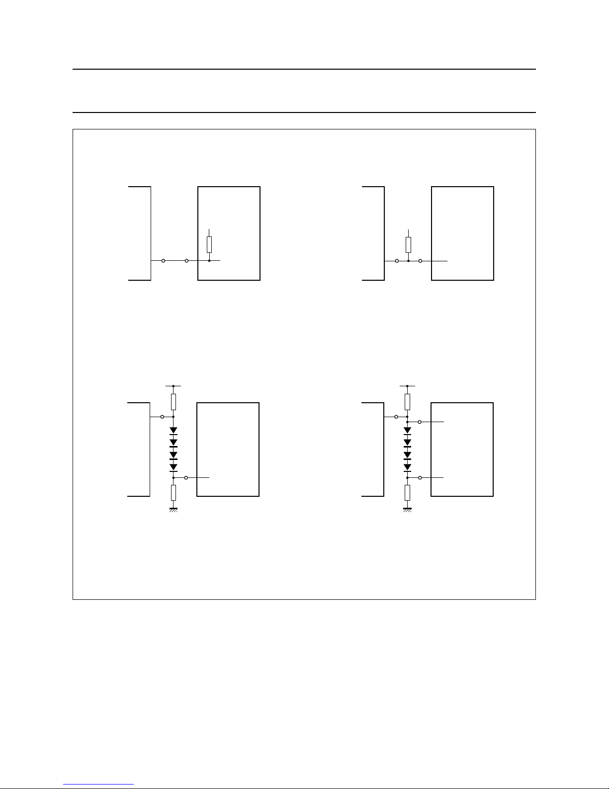
connected to a microcontroller. Figure 8 shows four
possible solutions for fault diagnosis.
Figures 8a and 8bshow simpleconfigurations. Theoutput
offset diagnostic cannot trigger the microcontroller
because of the 4-diode stack, only the temperature,
short-circuit and dynamic distortion diagnostic will give an
input LOW level for the microcontroller.
In Fig.8c, the diagnostic output is connected to an external
level shifter. Now DIAG pin output can also generate an
input LOW level for the microcontroller.
Assuming that a microcontroller HIGH input level must be
equal to, or greater than 2 V, the following equations are
used to calculate values for resistors R1 and R2:
V
IN1
> 2 V and
where:
5 V is the pull-up supply voltage
V
d
is the forward voltage of a diode (0.6 V)
R1 and R2 are the resistors in the level shifter.
Using both equations:
thus R1 > 3.3 R2
Therefore, R1 can be 47 kΩ and R2 can be 10 kΩ.
The level shifter shown in Fig.8d is used as a 2-bit
analog-to-digital converter.
With reference to Figs 7 and 8c, the truth table in Table 1
can be made:
Table 1 Truth table.
V
IN1
5V 4 VdR2
5V 4 V
d
×–
R1 R2+
-------------------------------
×–×–=
R1
2R2×
5V 4 V
d
2–×–
----------------------------------------
>
HIGH TEMPERATURE
OR SHORT-CIRCUIT OR
DDD
OFFSET IN1 IN2
no no 1 1
no yes 0 1
yes don’t care 0 0
handbook, halfpage
MGT610
≥1
DIAG
PGND
temperature diagnostic
short-circuit diagnostic
dynamic distortion detection
output offset diagnostic
Fig.7 Internal circuit diagnostic output pin DIAG.
Page 10
2002 Jan 14 10
Philips Semiconductors Preliminary specification
4 × 44 W into 4 Ω or 4 × 75 W into 2 Ω
quad BTL car radio power amplifier
TDA8591J
handbook, halfpage
MGU513
MICRO-
CONTROLLER
V
R
DIAG
handbook, halfpage
MGU514
MICRO-
CONTROLLER
V
R
DIAG
handbook, halfpage
MGU515
MICRO-
CONTROLLER
5 V
IN1
R1
R2
DIAG
handbook, halfpage
MGU516
MICRO-
CONTROLLER
5 V
IN1
R1
R2
IN2DIAG
Fig.8 Connecting the DIAG output to a microcontroller input.
a. Internal pull-up. b. External pull-up.
c. Level shifter. d. Two-pin diagnostics.
Page 11

2002 Jan 14 11
Philips Semiconductors Preliminary specification
4 × 44 W into 4 Ω or 4 × 75 W into 2 Ω
quad BTL car radio power amplifier
TDA8591J
7.3 Mute timer and single-pin mute control
Thetransition timefrom mute modeto operatingmodecan
be used to hide plops that occur during switching. This
transition time is determined by the value of the external
capacitor at the MUTE/ON input (see Fig.33). To
guarantee the mute suppression, the resistor value may
not be more than 15 kΩ. The switching can be controlled
by a transistor switch with an open-drain output or a
voltage output with a minimum high level of 5.5 V.
When controlling with an open-drain output, the high
voltage levelalso must be at least5.5 V and should notbe
clamped on a lower value by the ESD diode of the
microcontroller. If the minimum high voltage cannot be
guaranteed, an external open-drain transistor or switch to
ground can be used. Charging of theexternal capacitor at
the MUTE/ON input is done by an internal current source.
If muting is performed by the microcontroller, the mute
connection to the microcontroller can be omitted. The
mute on and off transitions during start-up and switch-off
are controlled by an internal push-pull current source and
the external capacitor at pin 8 (MUTE/ON).
Fast mute can be achieved by quickly discharging the
mute capacitor by means of an open-drain transistor
without a series resistor.
7.4 Output power
EIAJpower isapower ratingwhichindicates themaximum
possibleoutput powerofa specificapplicationat anominal
supply voltage. The power losses caused by PCB layout,
copper area, connector block, coil, loudspeaker wires, etc.
depend on the applications.
Therefore, theEIAJ power is defined and measured at the
pins of the IC using the following test conditions:
• The supply voltage is 14.4 V measured on the pins of
the TDA8591J
• All channels are loaded with 4 Ω and are driven
simultaneously
• The input signal is a continuous (no burst) square wave:
V = 1 V (RMS); f = 1 kHz
• RMS outputpower is measuredimmediately at the start
(cold heatsink) and after 1 minute of operation. The
mean value is the rated EIAJ power.
To have optimum output power performance, theexternal
heatsink should be chosen carefully. A small heatsink
causes a high junction temperature, resulting in an
increaseof thedrain-source on-stateresistance (R
DSon
)of
the power amplifiers and a decrease of the maximum
output power.
The reason for using a square wave input signal for EIAJ
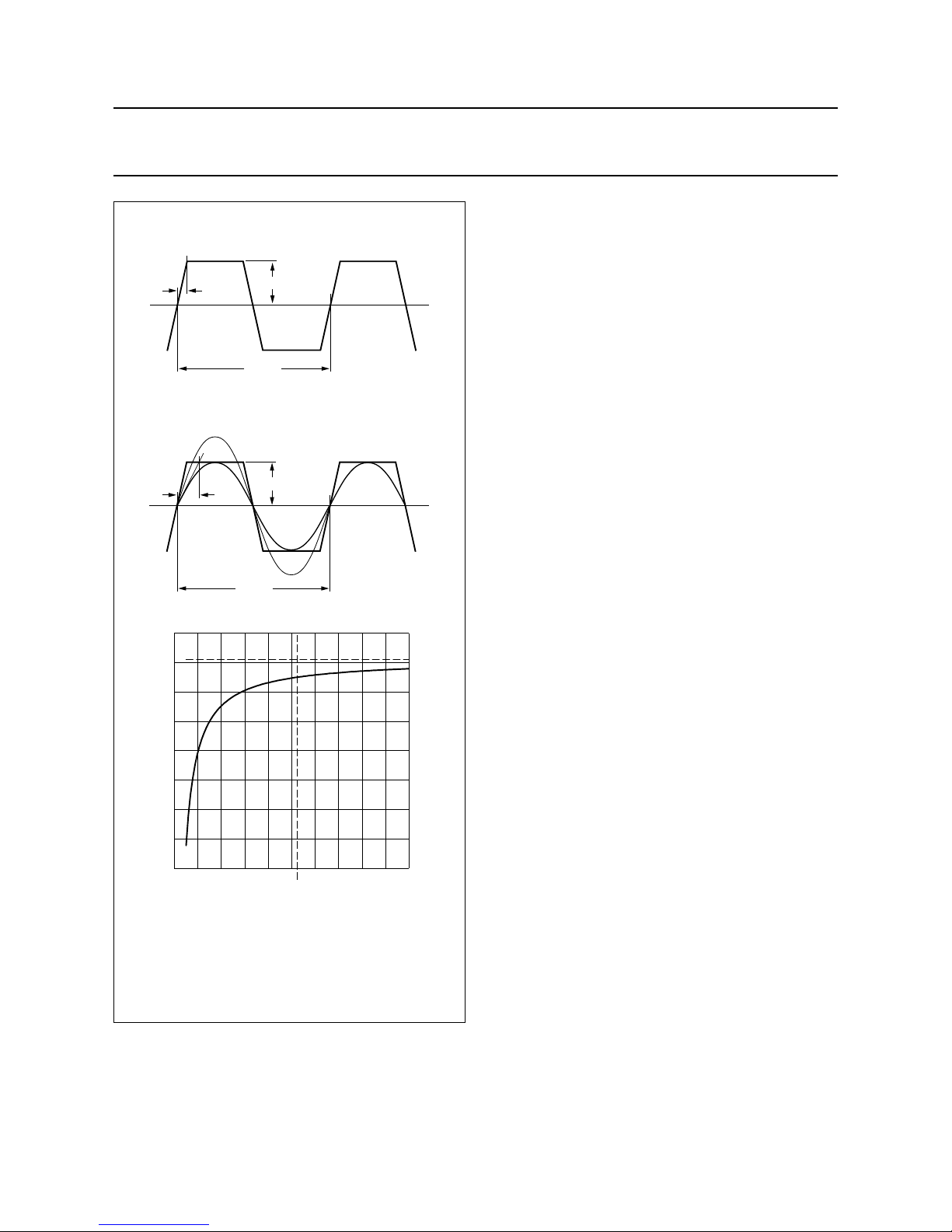
power measurement is illustrated in Fig.9.
Figure 9a shows a square wave signal with
Assuming this square wave is the output signal of an
amplifier, the EIAJ output power is given by
where:
R
L
= load resistor in Ω
V
top
= maximum voltage across the load in V
f = frequency of the square wave in Hz
tr= rise time of the slope in s.
A sine wave has a lower slew rate than a square wave as
shown in Fig.9b, therefore EIAJ power measurement with
a sine wave will give a lower power value. The maximum
slew rate of a sine wave output signal is given by
where:
A = amplitude of the output sinewave in V
f = frequency of the output sinewave in Hz.
For a non-clipping sinewave output with amplitude
A = 13 V and frequency f = 1 kHz, the slew rate is
A faster slew rate can be obtained by increasing the
amplitude: for an amplitude of 28 V, the slew rate will
increase to 1.85V/s. A supply voltage of VP= 14.4 V will
result in a clipped output with a shape similar to a square
wave but with a slower slew rate.
Figure 9c shows the dependency of P
EIAJ
on slew rate.
Using a square wave input signal, the EIAJ output power
is determined by the drop voltage and bandwidth of the
output stage.
slew rate
V
top
t
r
----------
=
P
EIAJ
V
top
2
R
L
-------------
1
8
3
-- -
V
top
× f×–
slew rate
------------------------------------------ -
×=
δ U
out
δt max
------------------
δ A sin× 2πft×()()
δt max
------------------------------------------------
2 πfA×==
δU
out
δt max
----------------- -
82
3
V/s=
Page 12
2002 Jan 14 12
Philips Semiconductors Preliminary specification
4 × 44 W into 4 Ω or 4 × 75 W into 2 Ω
quad BTL car radio power amplifier
TDA8591J
handbook, halfpage
MGT613
T = 1/f
V
top
t
r
handbook, halfpage
T = 1/f
V
top
t
r
MGT612
Fig.9 Comparison ofsine wave and square wave
RMS powers.
(1) P
EIAJ(max)
(infinite slew rate).
(2) Maximum slew rate of TDA8591J.
handbook, halfpage
0
45
43
44
42
41
2
P
EIAJ
(W)
10
MGT614
468
(2)
(1)
SR (V/µs)
a.
c.
b.
Page 13

2002 Jan 14 13
Philips Semiconductors Preliminary specification
4 × 44 W into 4 Ω or 4 × 75 W into 2 Ω
quad BTL car radio power amplifier
TDA8591J
8 LIMITING VALUES
In accordance with the Absolute Maximum Rating System (IEC 60134).
Notes
1. Human body model: C = 100 pF; R
s
= 1500 Ω; all pins have passed all tests to 2500 V to guarantee 2000 V,
according to
“General Quality Specification SNW-FQ-611D”
, class II, except pin GND, which passed 2200 V,
class Ia.
2. Machine model: C = 200 pF; Rs=10Ω; L = 0.75 mH.
SYMBOL PARAMETER CONDITIONS MIN. MAX. UNIT
V
P
supply voltage operating − 18 V
not operating −1 +45 V
with load dump protection (see Fig.10) − 45 V
V
DIAG
voltage on pin DIAG − 45 V
I
OSM
non-repetitive peak output
current
− 10 A
I
ORM
repetitive peak output current − 6A
V
sc
AC and DC short-circuit voltage short-circuit of output pins across
loads and to ground or supply
− 18 V
V
rp
reverse polarity voltage t ≤ 1ms − 6V
P
tot
total power dissipation T
case
=70°C − 80 W
T
vj
virtual junction temperature − 150 °C
T
stg
storage temperature −55 +150 °C
T
amb
ambient temperature −40 +85 °C
V
esd
electrostatic handling voltage note 1 2000 − V
note 2 200 − V
handbook, halfpage
MGT601
V
P
(V)
45
t
r
>2.5 ms
t
f
>47.5 ms
t
14.4
Fig.10 Load dump pulse definition.
Page 14
2002 Jan 14 14
Philips Semiconductors Preliminary specification
4 × 44 W into 4 Ω or 4 × 75 W into 2 Ω
quad BTL car radio power amplifier
TDA8591J
9 THERMAL CHARACTERISTICS
SYMBOL PARAMETER CONDITIONS VALUE UNIT
R
th(j-a)
thermal resistance from junction to ambient in free air 40 K/W
R
th(j-c)
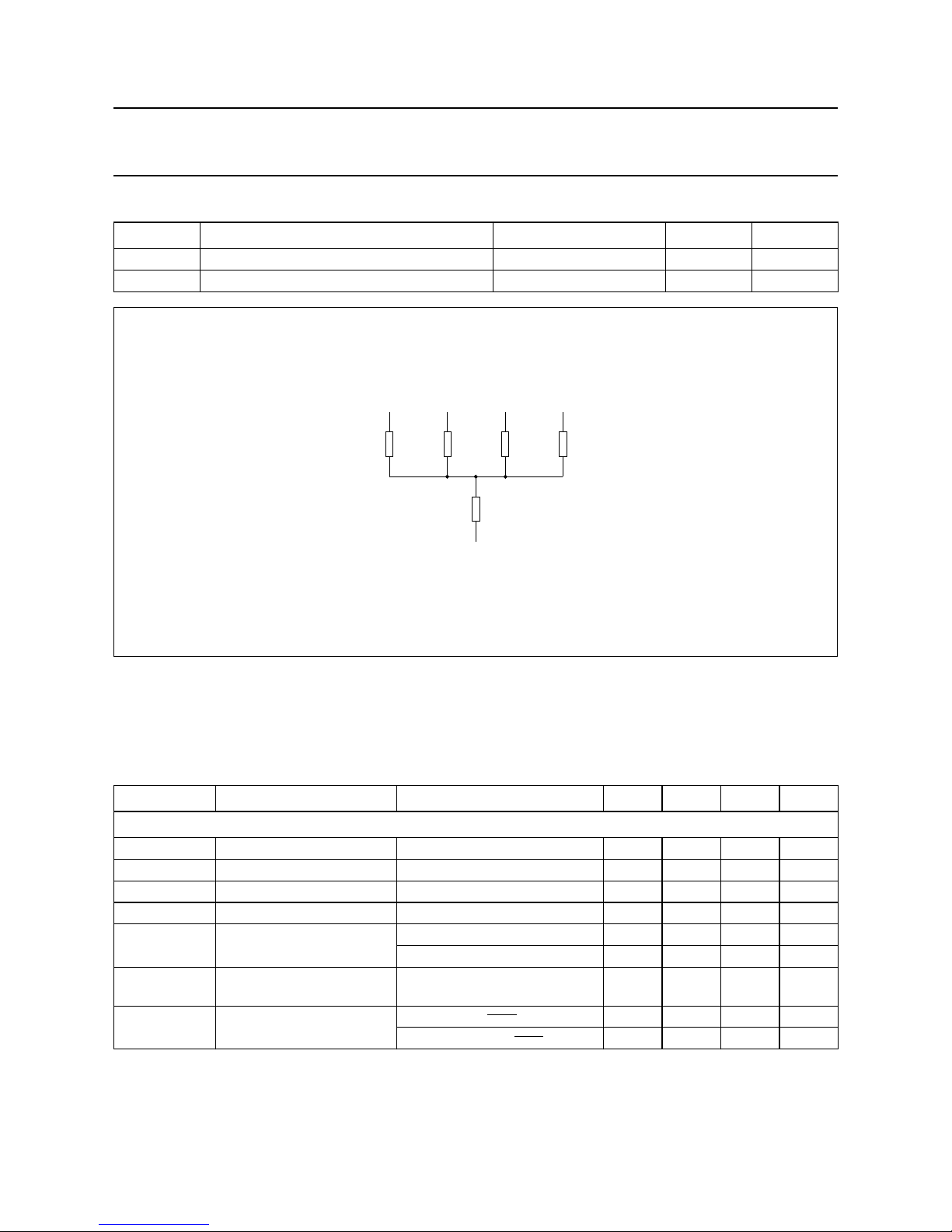
thermal resistance from junction to case see Fig.11 1 K/W
handbook, halfpage
2 K/W
0.5 K/W
2 K/W
2 K/W
2 K/W
virtual junction
OUT1 OUT2 OUT3 OUT4
case
MGT602
Fig.11 Equivalent thermal resistance network.
10 QUALITY SPECIFICATION
Quality according to
“SNW-FQ-611E”
.
11 DC CHARACTERISTICS
T
amb
=25°C; RL= ∞; VP=VP1=VP2=VP3= 14.4 V; measured in the circuit of Fig.29; unless otherwise specified.
SYMBOL PARAMETER CONDITIONS MIN. TYP. MAX. UNIT
Supplies
V
P
supply voltage 8.0 14.4 18.0 V
I
q(tot)
total quiescent current 120 200 290 mA
I
stb
standby current − 250µA
V
O
DC output voltage − 7.2 − V
V
P(mute)
low supply voltage mute operating to mute mode 6.0 7.0 8.0 V
mute to operating mode 6.3 7.0 8.5 V
V
P(mute)(hys)
low supply voltage mute
hysteresis
− 0.4 − V
V
OO
output offset voltage mute mode; V
MUTE/ON
=0V − 030mV
operating mode; V
MUTE/ON
=5V − 060mV
Page 15

2002 Jan 14 15
Philips Semiconductors Preliminary specification
4 × 44 W into 4 Ω or 4 × 75 W into 2 Ω
quad BTL car radio power amplifier
TDA8591J
Notes
1. With open MUTE/ON pin, the TDA8591J will switch to operating mode (see Section 7.3)
2. V
OO(det)
is the offset voltage across the load. Pin OFFCAP should never be left open-circuit. If pin OFFCAP is
connected to one of the PGND pins, the offset detection is switched off (see Section 14.4).
Table 2 Mode selection
STBY and
MUTE/ON inputs (see Table 2)
V
STBY
control voltage on pin STBY standby mode 0 − 0.8 V
V
STBY(hys)
voltage hysteresis on
pin STBY
− 0.2 − V
V
MUTE/ON
voltage on pin MUTE/ON mute mode; V
STBY
> 2.5 V −−0.8 V
operating mode; V
STBY
> 2.5 V;
note 1
5.5 − V
P
V
I
STBY
STBY pin current V
STBY
=5V −−80 µA
I
MUTE/ON
MUTE/ON pin current V
MUTE/ON
= 5.5 V − 25 −µA
DIAG output (see Figs 3 to 6)
V
DIAG
diagnostic output voltage I
DIAG(sink)
= 250 µA
DDD, protection circuits and
temperature pre-warning
active
− 0.3 0.8 V
offset diagnostic active 2.0 2.8 3.2 V
I
L
leakage current V
DIAG
= 14.4 V −−1µA
THD total harmonic distortion at
clip detection
V
DIAG
< 0.8 V − 1.5 − %
V
OO(det)
output offset voltage
detection; note 2
2.0<V
DIAG
< 3.2 V 2.5 4.5 6.5 V
T
vj
virtual junction temperature temperature pre-warning;
V
DIAG
< 0.8 V
135 145 −°C
soft thermal clipping;
G
v
= −3to−23 dB
− 155 −°C
temperature shut-down − 170 −°C
STBY
MUTE/ON AMPLIFIER MODE
0 don’t care standby (off)
1 0 mute (DC settled)
1 1 operating
SYMBOL PARAMETER CONDITIONS MIN. TYP. MAX. UNIT
Page 16

2002 Jan 14 16
Philips Semiconductors Preliminary specification
4 × 44 W into 4 Ω or 4 × 75 W into 2 Ω
quad BTL car radio power amplifier
TDA8591J
12 AC CHARACTERISTICS
V
P=VP1=VP2=VP3
= 14.4 V; RL=4Ω; f = 1 kHz; T
amb
=25oC; measured in the circuit of Fig.29; unless otherwise
specified.
Notes
1. The noise output voltage is measured in a bandwidth of 20 Hz to 20 kHz.
2. The frequency response is fixed with external components.
SYMBOL PARAMETER CONDITIONS MIN. TYP. MAX. UNIT
P
o
output power THD+N=0.5%
R
L
=4Ω 20 22 − W
R
L
=2Ω−34 − W
THD+N=1%; R
L
=2Ω− 35 − W
THD+N=10%
RL=4Ω 27 28 − W
R
L
=2Ω−47 − W
EIAJ values
RL=4Ω 41.5 44 W
R
L
=2Ω−75 − W
G
v
voltage gain Vi= 40 mV (RMS) 25 26 27 dB
THD + N total harmonic distortion plus
noise
P
o
= 1 W; f = 1 kHz − 0.03 0.1 %
P
o
= 10 W; f = 10 kHz − 0.2 − %
α
cs
channel separation Vi= 40 mV (RMS); Rs=0Ω 56 68 − dB
∆G
v
channel unbalance −−1dB
V
n(o)
noise output voltage Rs=0Ω; note 1
operating mode − 70 110 µV
mute mode − 16 −µV
V
o(mute)
output voltage in mute mode mute mode; Vi= 1 V (RMS) − 16 30 µV
SVRR supply voltage ripple rejection V
ripple
= 2 V (p-p); mute or
operating mode; Rs=0Ω
54 68 − dB
Z
i
input impedance Vi≤ 3 V (RMS) 60 70 − kΩ
CMRR common mode rejection ratio R
s
=0Ω;
Vcm= 0.35 V (RMS)
− 70 − dB
B
P
power bandwidth THD+N=0.5%; Po= −1dB
with respect to 17 W
− 20 to
20000
− Hz
f
ro(l)
low frequency roll-off at −1 dB; note 2 − 25 − Hz
f
ro(h)
high frequency roll-off at −1 dB 150 300 − kHz
Page 17

2002 Jan 14 17
Philips Semiconductors Preliminary specification
4 × 44 W into 4 Ω or 4 × 75 W into 2 Ω
quad BTL car radio power amplifier
TDA8591J
12.1 Performance curves
Conditions for Figs 12 to 28 unless otherwise specified are: VP= 14.4 V; RL=4Ω: f = 1 kHz; 80 kHz filter.
handbook, halfpage
0
300
200
100
0
30
MGW457
10 20
VP (V)
I
P
(mA)
Fig.12 Supply current as a function of supply
voltage.
RL= ∞.
handbook, halfpage
20
30
22
24
26
28
MGW458
10 10
2
10
3
10
4
10
5
f (Hz)
10
6
G
v
(dB)
Fig.13 Voltage gain as a function of frequency.
Vi=10mV.
handbook, halfpage
9
80
40
60
20
0
11 1210 18
MGW459
13 14 15 16 17
VP (V)
P
o
(W)
(1)
(2)
(3)
Fig.14 Output power as a function of supply
voltage; RL=4Ω.
One channel driven.
(1) EIAJ values.
(2) THD+N=10%.
(3) THD+N=1%.
handbook, halfpage
9
120
40
60
80
100
20
0
11 1210 18
MGW460
13 14 15 16 17
VP (V)
P
o
(W)
(1)
(2)
(3)
Fig.15 Output power as a function of supply
voltage; RL=2Ω.
One channel driven.
(1) EIAJ values.
(2) THD + N = 10%.
(3) THD + N = 1%.
Page 18
2002 Jan 14 18
Philips Semiconductors Preliminary specification
4 × 44 W into 4 Ω or 4 × 75 W into 2 Ω
quad BTL car radio power amplifier
TDA8591J
handbook, halfpage
−100
0
−80
−60
−40
−20
MGW461
10 10
2
10
3
10
4
f (Hz)
10
5
α
cs
(dB)
(1)
(2)
(3)
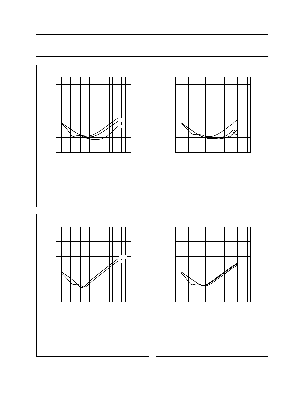
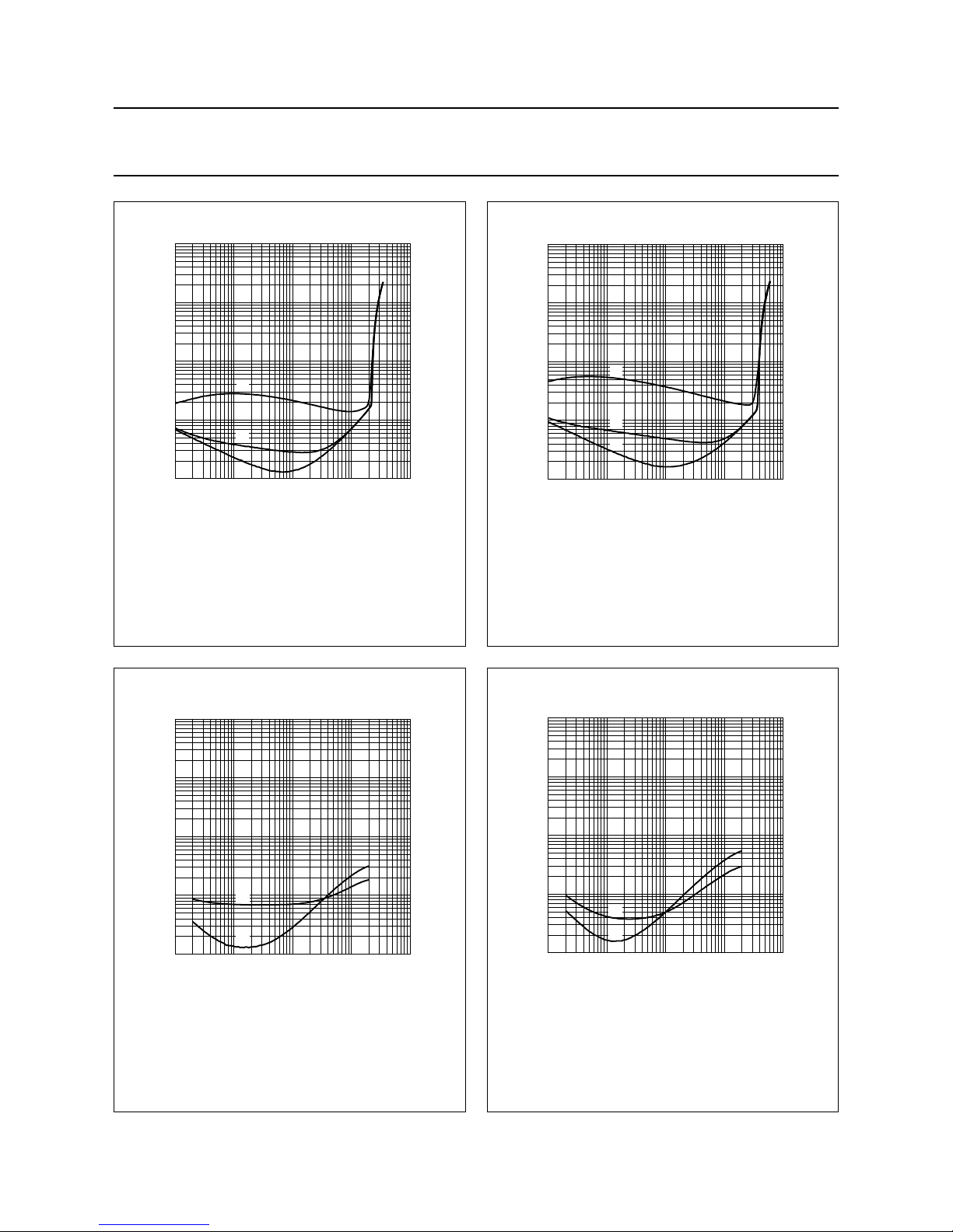
Fig.16 Channel separation as a function of
frequency; channel 1 driven.
Po= 1 W.
(1) Separation between channels 1 and 3.
(2) Separation between channels 1 and 4.
(3) Separation between channels 1 and 2.
handbook, halfpage
−100
0
−80
−60
−40
−20
MGW462
10 10
2
10
3
10
4
f (Hz)
10
5
α
cs
(dB)
(1)
(2)
(3)
Fig.17 Channel separation as a function of
frequency; channel 2 driven.
Po=1W.
(1) Separation between channels 2 and 1.
(2) Separation between channels 2 and 3.
(3) Separation between channels 2 and 4.
handbook, halfpage
−100
0
−80
−60
−40
−20
MGW463
10 10
2
10
3
10
4
f (Hz)
10
5
α
cs
(dB)
(1) (2)
(3)
Fig.18 Channel separation as a function of
frequency; channel 3 driven.
Po=1W.
(1) Separation between channels 3 and 1.
(2) Separation between channels 3 and 2.
(3) Separation between channels 3 and 4.
handbook, halfpage
−100
0
−80
−60
−40
−20
MGW464
10 10
2
10
3
10
4
f (Hz)
10
5
α
cs
(dB)
(1)
(2)
(3)
Fig.19 Channel separation as a function of
frequency; channel 4 driven.
Po=1W.
(1) Separation between channels 4 and 1.
(2) Separation between channels 4 and 2.
(3) Separation between channels 4 and 3.
Page 19
2002 Jan 14 19
Philips Semiconductors Preliminary specification
4 × 44 W into 4 Ω or 4 × 75 W into 2 Ω
quad BTL car radio power amplifier
TDA8591J
handbook, halfpage
10
2
10
THD + N
(%)
1
10
−1
10
−2
MGW465
10
−2
10
−1
110
P
o
(W)
10
2
(1)
(2)
(3)
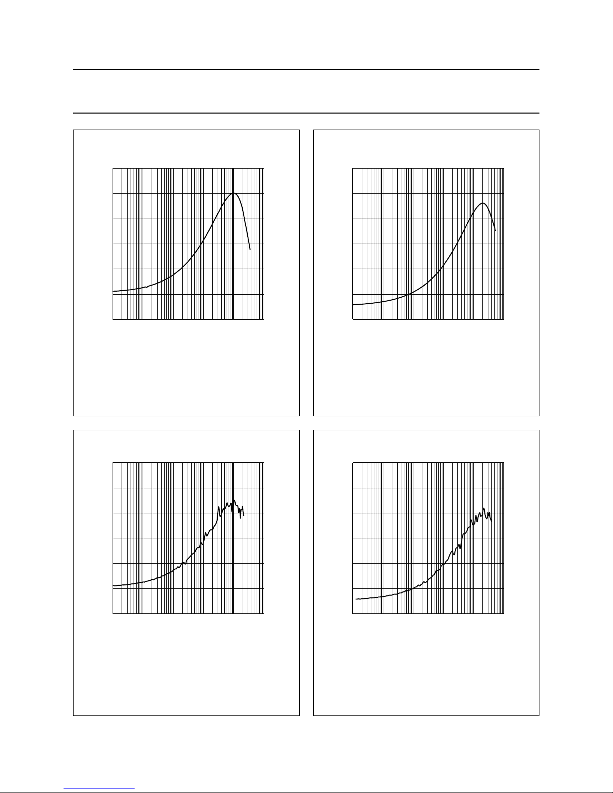
Fig.20 Total harmonic distortion plus noise as a
function of output power; RL=4Ω.
(1) f = 10 kHz.
(2) f = 1 kHz.
(3) f = 100 Hz.
handbook, halfpage
10
2
10
THD + N
(%)
1
10
−1
10
−2
MGW467
10
−2
10
−1
110
P
o
(W)
10
2
(1)
(2)
(3)
Fig.21 Total harmonic distortion plus noise as a
function of output power; RL=2Ω.
(1) f = 10 kHz.
(2) f = 1 kHz.
(3) f = 100 Hz.
handbook, halfpage
10
2
10
THD + N
(%)
1
10
−1
10
−2
MGW466
10 10
2
10
3
10
4
f (Hz)
10
5
(1)
(2)
Fig.22 Total harmonic distortion plus noise as a
function of frequency; RL=4Ω.
(1) Po=1W.
(2) Po=10W.
handbook, halfpage
10
2
10
THD + N
(%)
1
10
−1
10
−2
MGW468
10 10
2
10
3
10
4
f (Hz)
10
5
(1)
(2)
Fig.23 Total harmonic distortion plus noise as a
function of frequency; RL=2Ω.
(1) Po=1W.
(2) Po=10W.
Page 20
2002 Jan 14 20
Philips Semiconductors Preliminary specification
4 × 44 W into 4 Ω or 4 × 75 W into 2 Ω
quad BTL car radio power amplifier
TDA8591J
handbook, halfpage
MGW469
10
−2
1
P
(W)
Po (W)
10
−1
10 10
2
10
−3
15
10
5
0
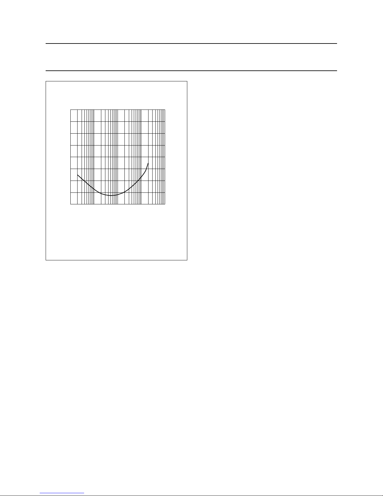
Fig.24 Power dissipation as a function of output
power; RL=4Ω.
Sine wave input; one channel driven.
handbook, halfpage
MGW470
10
−2
1
P
(W)
Po (W)
10
−1
10 10
2
10
−3
30
20
10
0
Fig.25 Power dissipation as a function of output
power; RL=2Ω.
Sine wave input; one channel driven.
handbook, halfpage
MGW471
10
−2
1
P
(W)
Po (W)
10
−1
10 10
2
10
−3
15
10
5
0
Fig.26 Power dissipation as a function of output
power; RL=4Ω.
IEC60268 filtered noise; one channel driven.
handbook, halfpage
MGW472
10
−2
1
P
(W)
Po (W)
10
−1
10 10
2
10
−3
30
20
10
0
Fig.27 Power dissipation as a function of output
power; RL=2Ω.
IEC60268 filtered noise; one channel driven.
Page 21
2002 Jan 14 21
Philips Semiconductors Preliminary specification
4 × 44 W into 4 Ω or 4 × 75 W into 2 Ω
quad BTL car radio power amplifier
TDA8591J
handbook, halfpage
−80
0
−60
−40
−20
MGW473
10 10
2
10
3
10
4
f (Hz)
10
5
SVRR
(dB)
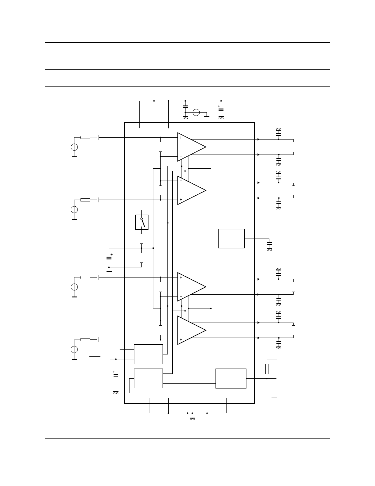
Fig.28 Supply voltageripple rejectionas afunction
of frequency.
V
ripple
= 2 V (p-p).
Page 22
2002 Jan 14 22
Philips Semiconductors Preliminary specification
4 × 44 W into 4 Ω or 4 × 75 W into 2 Ω
quad BTL car radio power amplifier
TDA8591J
13 TEST INFORMATION
handbook, full pagewidth
MGW451
26 dB
26 dB
26 dB
10
12
22
2
16
18
20
4
PGND1
8
3
5
26 dB
V
P
V
P
INTERFACE
OFFSET
DETECTION
7
PGND221PGND324PGND427GNDHS
DIAGNOSTIC
CHARGE
PUMP
TDA8591J
1
V
P1
13
V
P2
15
V
P3
4 Ω
22 nF
22 nF
OUT1−
OUT1+
9
11
4 Ω
22 nF
220 nF
22 nF
OUT2+
OUT2−
14 CP
6
DIAG
26 OFFCAP
19
17
4 Ω
22 nF
22 nF
OUT3+
OUT3−
25
23
4 Ω
10 kΩ
22 nF
22 nF
OUT4−
OUT4+
+5 V
R
s
V
in4
IN4
220 nF
R
s
V
in3
IN3
SGND
CIN
220 nF
R
s
V
in2
IN2
220 nF
R
s
V
in1
IN1
220 nF
100 µF
(6.3 V)
2200 µF
(16 V)
100
nF
V
cm
STBY
MUTE/ON
Fig.29 Test circuit.
Page 23
2002 Jan 14 23
Philips Semiconductors Preliminary specification
4 × 44 W into 4 Ω or 4 × 75 W into 2 Ω
quad BTL car radio power amplifier
TDA8591J
13.1 Protection circuit testing
handbook, full pagewidth
MGW453
4700 µF
>
100 µH
TDA8591J
(1)
battery
14.4 V
OUT−
−
+
OUT+
IN
STBY
GND
V
P
Fig.30 Open ground pin test set-up.
One channel output shown.
At the start of the test, the 4700 µF capacitor should be discharged.
The amplifier is in standby during test.
(1) Cable length is 1 metre, cable diameter is 1.5 mm.
handbook, full pagewidth
MGW454
4700 µF
>
100 µH
TDA8591J
(1)
battery
14.4 V
OUT−
−
+
OUT+
IN
STBY
GND
V
P
One channel output shown.
At the start of the test, the 4700 µF capacitor should be discharged.
The amplifier is in standby during test.
(1) Cable length is 1 metre, cable diameter is 1.5 mm.
Fig.31 Open power supply (pin VP) test set-up.
Page 24
2002 Jan 14 24
Philips Semiconductors Preliminary specification
4 × 44 W into 4 Ω or 4 × 75 W into 2 Ω
quad BTL car radio power amplifier
TDA8591J
handbook, full pagewidth
MGW455
4700 µF
>
100 µH
TDA8591J
(1)
battery
14.4 V
OUT−
−
+
OUT+
e.g.BZW03C18
IN
GND
fuse
V
P
Fig.32 Reversed polarity power supply test set-up.
(1) Cable length is 1 metre, cable diameter is 1.5 mm.
Page 25
2002 Jan 14 25
Philips Semiconductors Preliminary specification
4 × 44 W into 4 Ω or 4 × 75 W into 2 Ω
quad BTL car radio power amplifier
TDA8591J
14 APPLICATION INFORMATION
handbook, full pagewidth
MGW452
26 dB
26 dB
26 dB
10
12
22
2
16
18
20
4
PGND1
8
3
5
26 dB
V
P
V
P
INTERFACE
OFFSET
DETECTION
7
PGND2
21
PGND324PGND427GNDHS
DIAGNOSTIC
CHARGE
PUMP
TDA8591J
1
V
P1
13
V
P2
15
V
P3
22 nF
22 nF
OUT1−
OUT1+
9
11
22 nF
220 nF
22 nF
OUT2+
OUT2−
14 CP
6
DIAG
26 OFFCAP
19
17
22 nF
22 nF
OUT3+
OUT3−
25
23
2 or 4 Ω
22 nF
to microcontroller
22 nF
OUT4−
OUT4+
R
s
V
in4
IN4
220 nF
R
s
V
in3
IN3
SGND
CIN
220 nF
R
s
V
in2
IN2
220 nF
R
s
V
in1
IN1
220 nF
100 µF
(6.3 V)
2200 µF
(16 V)
100 nF
2 or 4 Ω
2 or 4 Ω
2 or 4 Ω
STBY
MUTE/ON
from
microcontroller
(1)
2.2
µF
(10 V)
mute
standby
fast mute
Fig.33 Quad BTL application without offset detection circuit.
(1) Not needed with single-pin mute control.
Page 26
2002 Jan 14 26
Philips Semiconductors Preliminary specification
4 × 44 W into 4 Ω or 4 × 75 W into 2 Ω
quad BTL car radio power amplifier
TDA8591J
handbook, full pagewidth
MGW476
26 dB
26 dB
26 dB
10
12
22
2
16
18
20
4
PGND1
8
3
5
26 dB
V
P
V
P
INTERFACE
OFFSET
DETECTION
7
PGND2
21
PGND324PGND427GNDHS
DIAGNOSTIC
CHARGE
PUMP
TDA8591J
1
V
P1
13
V
P2
15
V
P3
22 nF
22 nF
OUT1−
OUT1+
9
11
22 nF
220 nF
22 nF
OUT2+
OUT2−
14 CP
6
DIAG
26 OFFCAP
19
17
22 nF
22 nF
OUT3+
OUT3−
25
23
2 or 4 Ω
2 kΩ2 kΩ
22 nF
to microcontroller
22 nF
OUT4−
OUT4+
R
s
V
in4
IN4
220 nF
R
s
V
in3
IN3
SGND
CIN
220 nF
R
s
V
in2
IN2
220 nF
R
s
V
in1
IN1
220 nF
100 µF
(6.3 V)
2200 µF
(16 V)
1 µF
100 nF
2 or 4 Ω
2 or 4 Ω
2 or 4 Ω
220 kΩ
220 kΩ
220 kΩ
220 kΩ
STBY
MUTE/ON
from
microcontroller
(1)
2.2
µF
(10 V)
mute
standby
fast mute
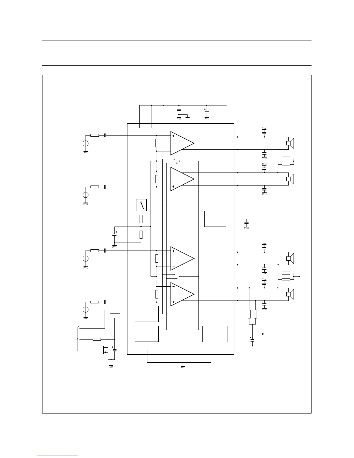
Fig.34 Quad BTL application with offset detection circuit.
(1) Not needed with single-pin mute control.
Page 27

2002 Jan 14 27
Philips Semiconductors Preliminary specification
4 × 44 W into 4 Ω or 4 × 75 W into 2 Ω
quad BTL car radio power amplifier
TDA8591J
14.1 Special attention for SMD input capacitors
When SMD capacitors are used as input capacitors, low
frequency noise can occur due to stress on the PCB. The
SMD capacitors can operate like small microphones with
sensitivity of
1
⁄f. Special attention should be paid to this
issue when selecting SMD capacitors at the four inputs
(MKT capacitors are recommended).
14.2 Capacitors on outputs
The TDA8591J is optimized for a capacitor of 22 nF from
each output to ground for RF immunity and ESD. These
capacitors can be replaced by the capacitors on the
connector block.
14.3 EMC precautions
The TDA8591J has an all N-type DMOS output stage. The
main advantage of having the same type of power
transistorsin theoutput stageis symmetricalbehaviour for
positive and negative signals (sound quality).
A charge pump (DC to DC converter with capacitors only)
is used to generate a voltage above the battery voltage to
drive the high-side power. The clock frequency of the
charge pump (2.9 MHz) is chosen above the AM
frequency band. To prevent possible crosstalk in the FM
frequency band, a SIL pad can be used between the rear
of the TDA8591J and the heatsink. This SIL pad is an
electrical isolator and thermal conductor. It is advisable to
connectthe powersupply lines ofthe TDA8591Jdirectlyto
the power supply on the printed circuit board of the radio,
so that a one-point earth bonding with the tuner supply is
achieved.
The external capacitor of the charge pump (connected to
pin CP)filters andbuffers thevoltage generatedinternally.
The loop area of the capacitor connected to pins CP and
PGND2 shouldbe kept assmall as possible. For optimum
performance the capacitor used should have a good
frequency performance, for example an SMD ceramic
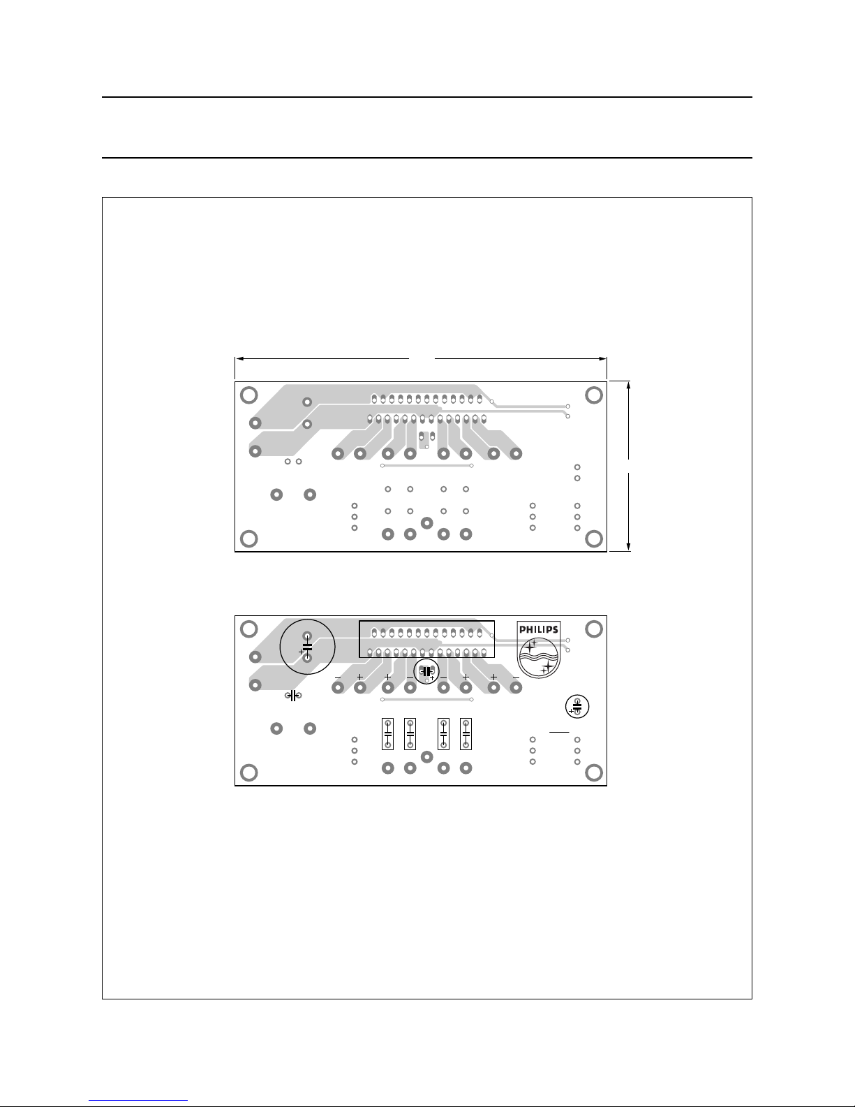
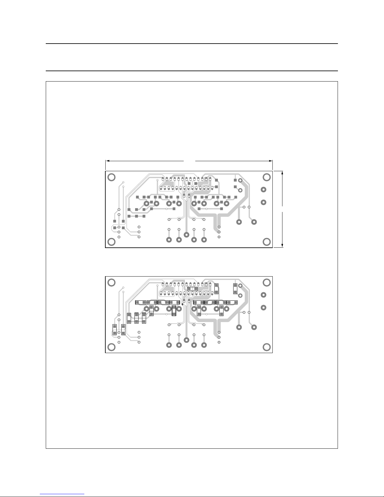
capacitor. See Figs 35 and 36 for a good PCB layout.
14.4 Offset detection
As shown in Fig.34, to obtain the DC offset information, an
output from each bridge is summed and filtered through
external 220 kΩ resistors and a 1 µF capacitor at
pin OFFCAP. The low frequency roll-off can be chosen
with the resistor/capacitor combination. Because of the
random phase of the DC offset voltage, the capacitor on
pin OFFCAP should not be a conventional electrolytic
capacitor asleakage current inthis capacitor would cause
a shift in low frequency roll-off because of no pre-biasing.
If the offset detection is not used, pin OFFCAP can be
connected to ground, the external components (resistors
of 220 kΩ and 2 kΩ and the capacitor of 1µF) are not
needed and the circuit is as shown in Fig.33.
14.5 Channel selection
The following recommendation for a four channel
application is given on the basis of the results of the
channel separation measurements and the dissipation
spread within the package:
Front-left = OUT1
Rear-left = OUT2
Rear-right = OUT3
Front-right = OUT4.
14.6 Detection of short-circuits
Table 3 Detection of short-circuits in standby, mute and operating modes.
AMPLIFIER MODE SHORT-CIRCUIT ACROSS LOAD
SHORT-CIRCUIT TO SUPPLY
OR GROUND
Standby no diagnosis no diagnosis
Mute (no output signal) the value of short-circuit that activates
diagnosis and protection depends on
the output offset voltage
no diagnosis andno active protection if
short-circuit >100 Ω
Operating (output signal present) diagnosis and active protection if
short-circuit <0.4 Ω
no diagnosis andno active protection if
short-circuit >100 Ω
Page 28
2002 Jan 14 28
Philips Semiconductors Preliminary specification
4 × 44 W into 4 Ω or 4 × 75 W into 2 Ω
quad BTL car radio power amplifier
TDA8591J
14.7 PCB layout
handbook, full pagewidth
gnd
gnddiag
float
sgnd
sgnd
PCB
On
Mute
TDA8591J
Off
GND
Out1 Out2 Out3 Out4
2.2 µF
In1 In3In2 In4
8-18V
V
P
MGW474
85.1
39.4
Fig.35 PCB layout (component side).
Dimensions in mm.
Page 29
2002 Jan 14 29
Philips Semiconductors Preliminary specification
4 × 44 W into 4 Ω or 4 × 75 W into 2 Ω
quad BTL car radio power amplifier
TDA8591J
handbook, full pagewidth
22 nF
1 µF
GND
V
P
47 kΩ
47 kΩ15 kΩ
220 kΩ
2 kΩ 2 kΩ
220 kΩ 220 kΩ 220 kΩ
27
22 nF 22 nF
220 nF220 nF
22 nF 22 nF 22 nF 22 nF 22 nF
MGW475
39.4
85.1
Fig.36 PCB layout (soldering side).
Dimensions in mm.
Page 30
2002 Jan 14 30
Philips Semiconductors Preliminary specification
4 × 44 W into 4 Ω or 4 × 75 W into 2 Ω
quad BTL car radio power amplifier
TDA8591J
14.8 PCB design advice
handbook, full pagewidth
MGW456
10IN1
PCB SGND
DIAG
(3)
(8)
(4)
(5)
3.3
nF
220 nF
(2)
220 nF
(1)
2
kΩ
47
kΩ
47
kΩ
15
kΩ
2
kΩ
TDA8591J
(7)
(6)
220 nF
22 nF
12
IN2
220 nF
16
IN3
220 nF
18
20 8
3
5
6
2
22
IN4
220 nF
2200 µF
(16 V)
1 1315 14 7 4 212427
26
OUT1−
22 nF
OUT1+
22 nF
9
11
OUT2+
22 nF
OUT2−
22 nF
19
17
OUT3+
22 nF
OUT3−
22 nF
25
23
OUT4+
22 nF
0.22
(9)
R R R R
OUT4−
GND
V
P
8 to 18 V
2.2 µF
(6.3 V)
100 µF
(6.3 V)
R
C =
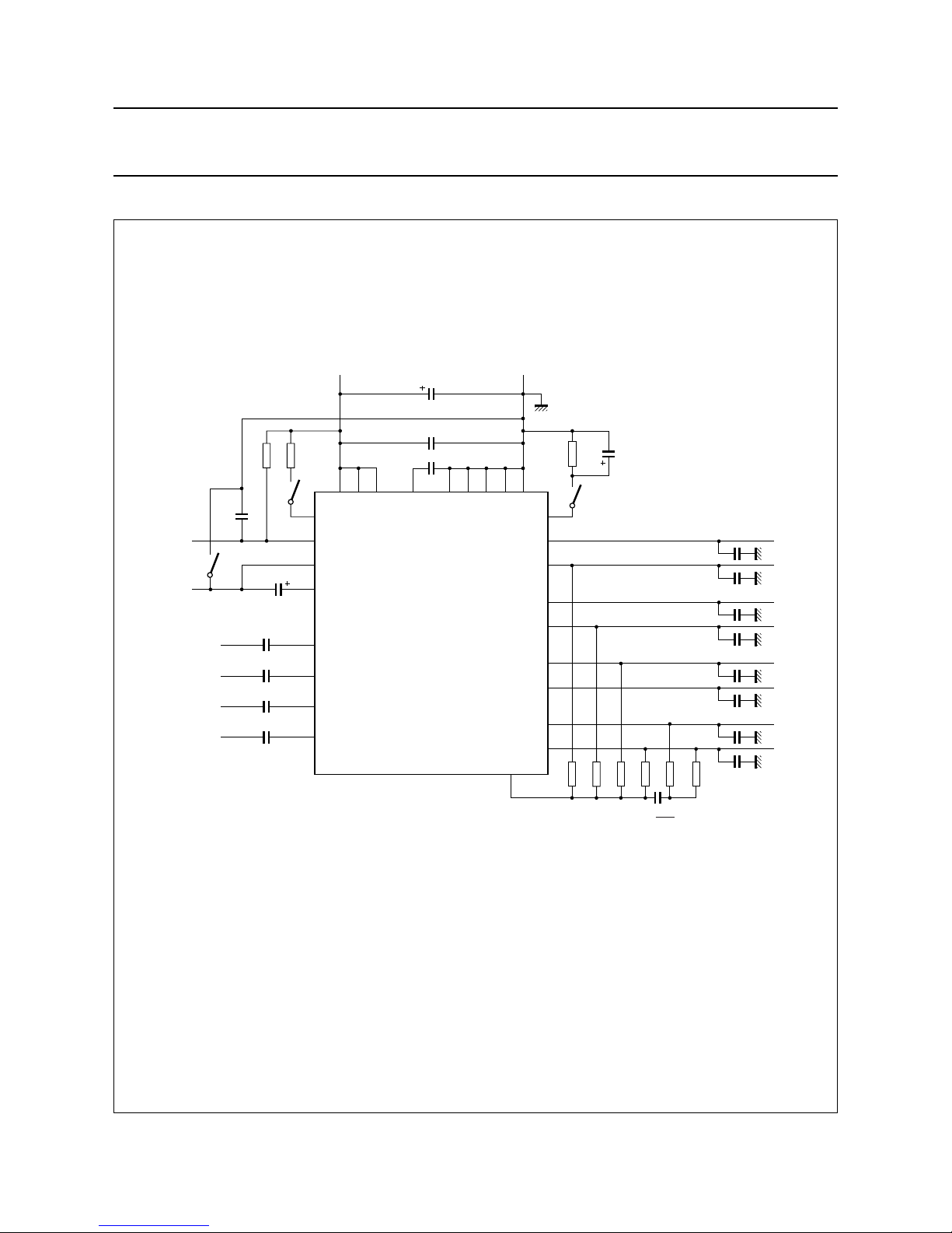
Fig.37 PCB design advice.
(1) Power supply high frequency capacitor to be mounted close to the IC. An SMD component is recommended.
(2) Charge pump capacitor to be mounted close to the IC between pins 14 and 7.
(3) Switch closed is the mute mode.
(4) Switch open is the standby mode.
(5) A 3.3 nF capacitor has been added to provide a smooth offset detection diagnostic.
(6) Diagnostic output is less than 0.8 V when DDD or temperature pre-warning or protection circuits are activated.
(7) Signal ground switch is closed if the source is floating. Avoid ground loops in the input signal path. Keep inputs and signal ground close together.
(8) The 22 nF capacitors on the outputscan bereplaced bythe capacitoron theconnector blockto ground,where itis often usedfor RF immunity and
ESD suppression.
(9) Offset detection:if R = 100 kΩ then C = 2.2 nF; if R = 220 kΩ then C = 1 µF. An electrolytic capacitor is not allowed becauseof the random phase
of the DC offset.
Page 31
2002 Jan 14 31
Philips Semiconductors Preliminary specification
4 × 44 W into 4 Ω or 4 × 75 W into 2 Ω
quad BTL car radio power amplifier
TDA8591J
15 PACKAGE OUTLINE
UNIT A A
2
REFERENCES
OUTLINE
VERSION
EUROPEAN
PROJECTION
ISSUE DATE
IEC JEDEC EIAJ
mm
17.0
15.5
4.6
4.3
A
4
1.15
0.85
A
5
1.65
1.35
DIMENSIONS (mm are the original dimensions)
Note
1. Plastic or metal protrusions of 0.25 mm maximum per side are not included.
SOT521-1
0 5 10 mm
scale
L
E
A
c
A
4
A
5
A
2
m
L
3
E
1
Q
w M
b
p
1
d
Z
e
2
e
e
127
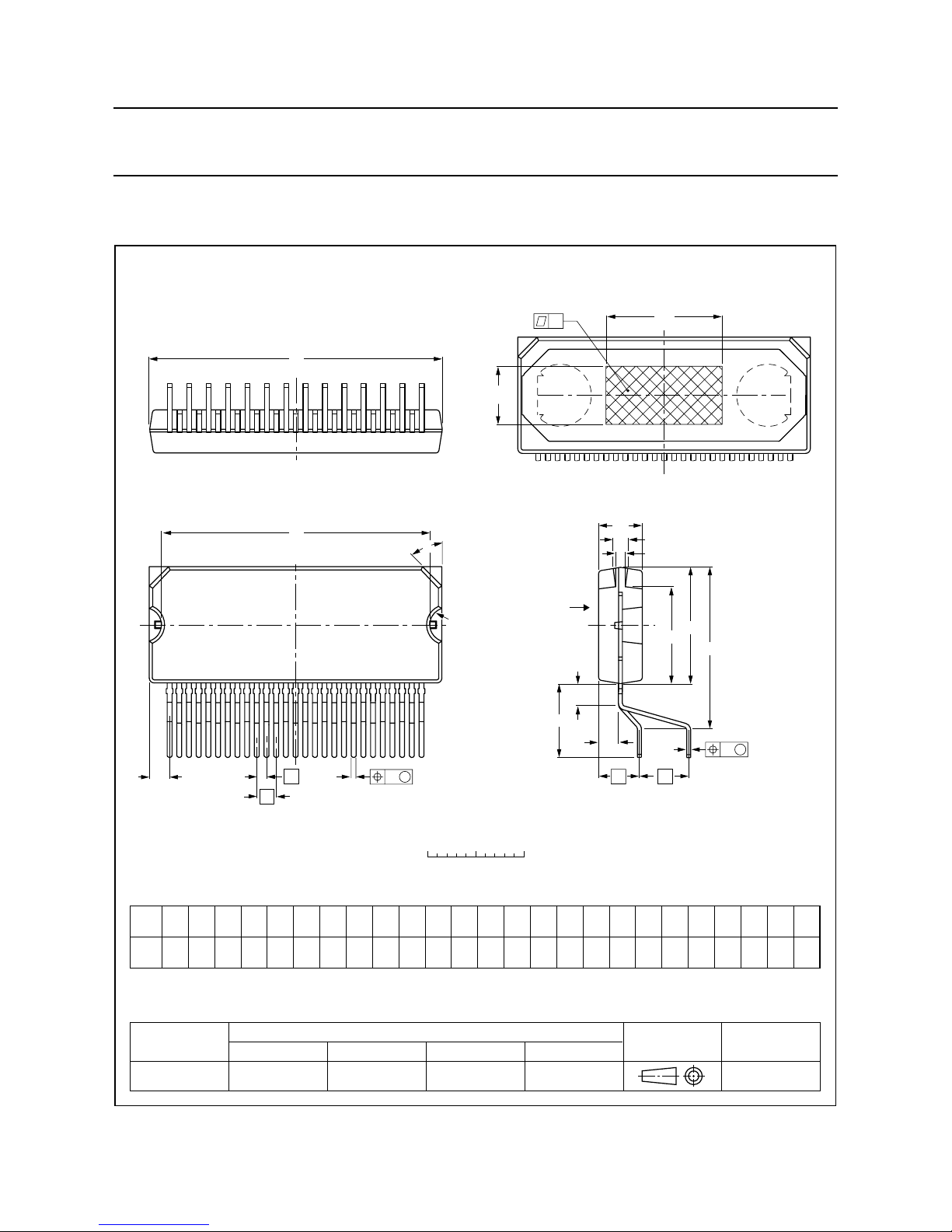
DBS27P: plastic DIL-bent-SIL power package; 27 leads (lead length 7.7 mm)
SOT521-1
v M
D
x
h
E
h
non-concave
view B: mounting base side
B
D
β
e
1
bpcD
(1)
E
(1)
Z
(1)
deD
h
LL3m
0.60
0.45
0.5
0.3
30.4
29.9
28.0
27.5
12 2.0
12.2
11.8
10.15
9.85
1.0
e
2
4.0
2.4
1.6
E
h
6
E
1
2.4
1.8
2.1
1.8
1.85
1.65
4.3
8.4
7.0
Qj
0.25
w
0.6
v
0.03x45°
β
j
99-01-05
Page 32

2002 Jan 14 32
Philips Semiconductors Preliminary specification
4 × 44 W into 4 Ω or 4 × 75 W into 2 Ω
quad BTL car radio power amplifier
TDA8591J
16 SOLDERING
16.1 Introduction to soldering through-hole mount
packages
This text gives a brief insight to wave, dip and manual
soldering.A morein-depth account ofsoldering ICscanbe
found in our
“Data Handbook IC26; Integrated Circuit
Packages”
(document order number 9398 652 90011).
Wave soldering is the preferred method for mounting of
through-hole mount IC packages on a printed-circuit
board.
16.2 Soldering by dipping or by solder wave
The maximum permissible temperature of the solder is
260 °C; solder at this temperature must not be in contact
with the joints for more than 5 seconds.
Thetotal contacttimeof successivesolderwaves mustnot
exceed 5 seconds.
The device may be mounted up to the seating plane, but
the temperature of the plastic body must not exceed the
specified maximum storage temperature (T
stg(max)
). If the
printed-circuit board has been pre-heated, forced cooling
may benecessary immediately after soldering to keep the
temperature within the permissible limit.
16.3 Manual soldering
Apply the soldering iron (24 V or less)to the lead(s) of the
package, either below the seating plane or not more than
2 mm above it. If the temperature of the soldering iron bit
is less than 300 °C it may remain in contact for up to
10 seconds. If the bit temperature is between
300 and 400 °C, contact may be up to 5 seconds.
16.4 Suitability of through-hole mount IC packages for dipping and wave soldering methods
Note
1. For SDIP packages, the longitudinal axis must be parallel to the transport direction of the printed-circuit board.
PACKAGE
SOLDERING METHOD
DIPPING WAVE
DBS, DIP, HDIP, SDIP, SIL suitable suitable
(1)
Page 33

2002 Jan 14 33
Philips Semiconductors Preliminary specification
4 × 44 W into 4 Ω or 4 × 75 W into 2 Ω
quad BTL car radio power amplifier
TDA8591J
17 DATA SHEET STATUS
Notes
1. Please consult the most recently issued data sheet before initiating or completing a design.
2. The product status of the device(s) described in this data sheet may have changed since this data sheet was
published. The latest information is available on the Internet at URL http://www.semiconductors.philips.com.
DATA SHEET STATUS
(1)
PRODUCT
STATUS
(2)
DEFINITIONS
Objective data Development This data sheet contains data from the objective specification for product
development. Philips Semiconductors reserves the right to change the
specification in any manner without notice.
Preliminary data Qualification This data sheet contains data from the preliminary specification.
Supplementary data will be published at a later date. Philips
Semiconductors reserves the right to change the specification without
notice, in order to improve the design and supply the best possible
product.
Product data Production This data sheet contains data from the product specification. Philips
Semiconductors reserves the right to make changes at any time in order
to improve the design, manufacturing and supply. Changes will be
communicated according to the Customer Product/Process Change
Notification (CPCN) procedure SNW-SQ-650A.
18 DEFINITIONS
Short-form specification The data in a short-form
specification is extracted from a full data sheet with the
same type number and title. For detailed information see
the relevant data sheet or data handbook.
Limiting valuesdefinition Limiting values givenare in
accordance with the Absolute Maximum Rating System
(IEC 60134). Stress above one or more of the limiting
values may cause permanent damage to the device.
These are stress ratings only and operation of the device
atthese orat any otherconditions above thosegiven inthe
Characteristics sectionsof the specification isnot implied.
Exposure to limiting values for extended periods may
affect device reliability.
Application information Applications that are
described herein for any of these products are for
illustrative purposes only. Philips Semiconductors make
norepresentation orwarranty thatsuchapplications willbe
suitable for the specified use without further testing or
modification.
19 DISCLAIMERS
Life support applications These products are not
designed for use in life support appliances, devices, or
systems where malfunction of these products can
reasonably be expected to result in personal injury. Philips
Semiconductorscustomers using orselling these products
for use in such applications do so at their own risk and
agree to fully indemnify Philips Semiconductors for any
damages resulting from such application.
Right to make changes Philips Semiconductors
reserves the right to make changes, without notice, in the
products, including circuits, standard cells, and/or
software, described or contained herein in order to
improve design and/or performance. Philips
Semiconductors assumes no responsibility or liability for
theuse ofanyof theseproducts,conveys nolicenceor title
under any patent, copyright, or mask work right to these
products,and makesno representations orwarranties that
these products are free from patent, copyright, or mask
work right infringement, unless otherwise specified.
Page 34

2002 Jan 14 34
Philips Semiconductors Preliminary specification
4 × 44 W into 4 Ω or 4 × 75 W into 2 Ω
quad BTL car radio power amplifier
TDA8591J
NOTES
Page 35

2002 Jan 14 35
Philips Semiconductors Preliminary specification
4 × 44 W into 4 Ω or 4 × 75 W into 2 Ω
quad BTL car radio power amplifier
TDA8591J
NOTES
Page 36

© Koninklijke Philips Electronics N.V. 2002
SCA74
All rights are reserved. Reproduction in whole or in part is prohibited without the prior written consent of the copyright owner.
The information presented in this document does not form part of any quotation or contract, is believed to be accurate and reliable andmay be changed
without notice. No liability will be accepted by the publisher for any consequence of its use. Publication thereof does not convey nor imply any license
under patent- or other industrial or intellectual property rights.
Philips Semiconductors – a w orldwide compan y
Contact information
For additional information please visit http://www.semiconductors.philips.com. Fax: +31 40 27 24825
For sales offices addresses send e-mail to: [email protected].
Printed in The Netherlands 753503/01/pp36 Date of release: 2002 Jan 14 Document order number: 9397 750 08682
 Loading...